Intel Adds Crystal Well-based Skylake-R Processors: 65W with 128MB eDRAM
by Anton Shilov on May 2, 2016 4:30 PM EST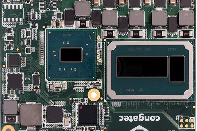
Intel has added three new microprocessors for embedded and highly-integrated applications into its lineup. The new CPUs are based on the Skylake microarchitecture and feature high-performance integrated graphics cores with an added eDRAM cache called Crystal Well. The new products should offer high performance in memory bandwidth applications due to Skylake’s updated 2nd generation cache architecture.
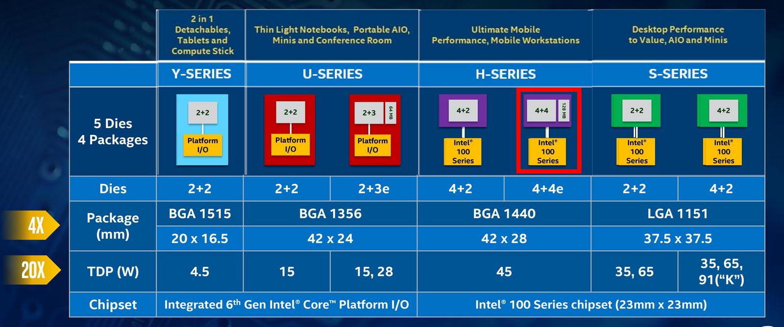
In red is the 4+4e die with 128MB eDRAM
The chips that Intel has added to its price list are the Core i7-6785R, the Core i5-6685R, and the Core i5-6585R. The new processors are designed to fit in all-in-one PCs, small form-factor and other types of highly-integrated PCs that can satisfy the 65W TDP over the mobile Crystal Well variants that run at 45W. The new desktop chips from Intel are based on the Skylake-H silicon in its most advanced configuration: with four general-purpose cores as well as the GT4e integrated graphics. Not all the specifications of the processors are known at this point, but we are talking about quad-core processors with Generation 9 Iris Pro graphics and 72 execution units (as well as 128 MB of eDRAM), a dual-channel DDR4-2133 memory controller, a PCI Express 3.0 interface and three display outputs. The power consumption of Intel’s new embedded products for desktops does not exceed 65 W, which is typical for R-series offerings, and offer a potential upgrade path by OEMs for any equivalent systems that used an equivalent Broadwell-based R-series processor.
Intel unveiled its Skylake-H silicon in its full glory earlier this year when it released its mobile Xeon E3 v5 processors with the Iris Pro Graphics P580.
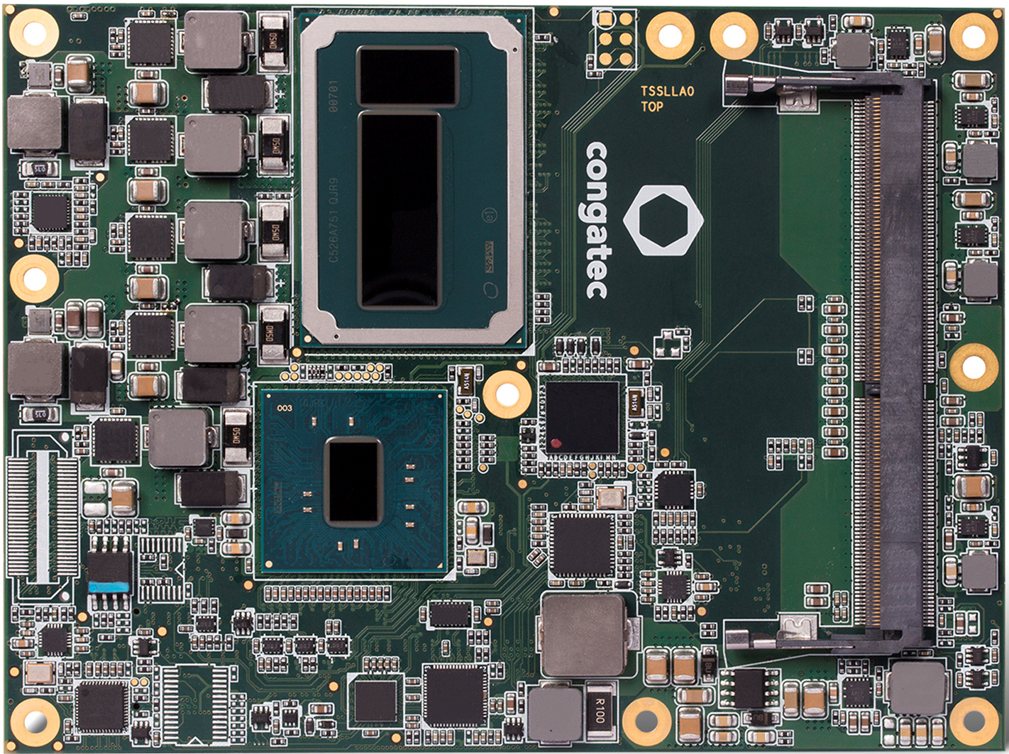
Several makers of industrial computer modules (such as Congatec) already use chips like the Intel Xeon E3-1515M v5 for their products, which is why we know what they look like. The die of the Skylake-H processor looks rather long and the lion’s portion of its transistor budget was spent on the mammoth iGPU. The extra on package die is the eDRAM, and the silicon underneath the CPU is the chipset (it's the Y/U series CPUs that have integrated chipsets).
| Comparison of Intel's Embedded CPUs | |||||||||
| i7-6785R | i5-6685R | i5-6585R | i7-5775R | i5-5675R | i5-5575R | ||||
| Microarchitecture | Skylake | Broadwell | |||||||
| Cores/Threads | 4 / 8 | 4 / 4 | 4 / 4 | 4 / 8 | 4 / 4 | 4 / 4 | |||
| L2 Cache | 1 MB (256 KB × 4) | ||||||||
| L3 Cache | 8 MB | 6 MB | 6 MB | 4 MB | |||||
| eDRAM | 128 MB | 128 MB | |||||||
| CPU Frequency | default | 3.30 GHz | 3.20 GHz | 2.80 GHz | 3.30 GHz | 3.10 GHz | 2.80 GHz | ||
| maximum | 3.90 GHz | 3.80 GHz | 3.60 GHz | 3.80 GHz | 3.60 GHz | 3.30 GHz | |||
| GPU | Iris Pro 580 | Iris Pro 6200 | |||||||
| EUs | 72 | 48 | |||||||
| TDP | 65 W | 65 W | |||||||
| GPU Frequency | 350 MHz to 1150/1150/1100 MHz | 300 MHz to 1150/1100/1050 MHz | |||||||
| DRAM Support | DDR4-2133/1866 DDR3L-1600/1333 |
- DDR3L-1866/1600/1333 |
|||||||
| Packaging | FCBGA1440 | FCBGA1364 | |||||||
| Process Technology | 14 nm | ||||||||
| Price | $370 | $288 | $255 | $348 | $265 | $244 | |||
The new parts feature higher clock rates compared to the Broadwell processors, although slightly lower than their K series counterparts. The processors have a number of important architectural improvements which will affect the performance of these CPUs in real-world applications. It is interesting to note that Intel retained the full L3 cache size in its new R-series CPUs: in the Broadwell models part of the L3 was used for eDRAM tags, reducing their capacity by 2 MB, but the new Skylake parts are now in line with their i7 and i5 naming due to the way the eDRAM is implemented. This means that the i7-6785R has 8 MB of L3, similar to the i7-6700K, and the i5-6685R/6585R has 6 MB of L3, similar to the i5-6600K.
Intel’s Skylake processors feature an upgraded microarchitecture with better parallelism and improved IPC, which means better performance almost across-the-board. An important capability of Skylake is its Speed Shift technology, which can quickly increase frequency for a short amount of time in a bid to rapidly perform an operation (~1-3 milliseconds rather than 30-100 without Speed Shift), thus providing better user experience and ultimately saving power. Intel’s Speed Shift requires support by the operating system and right now Microsoft’s Windows 10 can take advantage of the technology in a bid to improve its responsiveness.

Another important aspect of Intel’s Skylake CPUs with high-end iGPUs is their eDRAM, which means the processors also gain the code name 'Crystal Well'. The eDRAM for Skylake is different to that found in previous Crystal Well implementations: in the last generation, the eDRAM acted as a victim cache to the L3 cache, meaning that evicted cache lines from L3 would add up in the eDRAM and be quick for re-reading without having to access main memory. The downside to this is that data could not end up in eDRAM without being used first, giving initial data read latencies the same performance as previous processors. Ultimately this is still good for graphics and gaming, where textures are re-read from memory frequently. The new arrangement for the eDRAM in these Skylake processors has placed the eDRAM in a different part of the chain, between the System Agent and the DDR memory. This means that the eDRAM acts as a DRAM buffer, with 50 GBps bandwidth in each direction to the LLC, but is also accessible for early reads/writes by any device that needs memory access through the system agent (i.e. anything through PCIe). Previously this was not possible, but now it means that Skylake's eDRAM implementation should offer a speedup in many more scenarios that before.
The final noteworthy improvement of the Skylake processors compared to previous-generation offerings is revamped graphics core as well as increased amount of execution units. Based on our findings last year, real-world performance of Intel's high-end Iris Pro 6200 graphics core (Broadwell’s top iGPU) is higher than that of entry-level discrete graphics cards. Meanwhile, the highest-performing GT4e graphics core of Intel Skylake contains 72 EUs, up from 48 in the case of the Broadwell. Compute performance of Intel's contemporary top-of-the-range iGPU (Iris Pro 580) is around 1.1 TFLOPS depending on its frequency, so, this one should be tangibly faster than its predecessor. Last, but not least, Skylake’s iGPU has a revamped multimedia engine, which supports hardware decoding and encoding of UHD videos using HEVC or VP9 codecs.
Intel’s new Core i7-6785R, Core i5-6685R, and Core i5-6585R are already available at a tray price of $370, $288 and $255 respectively. Partners of the chipmaker will likely use the new processors to build their new systems in the coming months.
Image Sources: Congatec, Intel's IDF presentations.
Source: Intel's Price List (via a reader)


67 Comments
View All Comments
ddriver - Monday, May 2, 2016 - link
AT without addblock is just too disgusting, with addblock only moderately so :)madwolfa - Monday, May 2, 2016 - link
I'm trying to support them, but this was over the top.lilmoe - Tuesday, May 3, 2016 - link
It really is. It's frustrating. It's like when you want to support someone but they'd always jumps on your shoulders on the slightest smile you give them...wow&wow - Monday, May 2, 2016 - link
"Intel adds ... eDRAM"eDRAM is for DRAM that is integrated on the same die, i.e. monolithic.
Intel's solution is call hybrid, multiple dies on the same package substrate.
Others may be able to differentiate, but Anatech should : (
wow&wow - Monday, May 2, 2016 - link
Oops, correction:Others may not be able to differentiate, but Anatech should : (
Ian Cutress - Tuesday, May 3, 2016 - link
Intel officially calls it eDRAM, whether it's a multi-die package or not.It's the modular nature of this feature, rather than create another two separate monolithic dies in their product stack. Even if you consider this to not be 'a true eDRAM' representation, it acts as one for all intents and purposes. If it was integrated on die, chances are it would be made into a true L4, but it would also have to be designed into a combined rectangular die for production efficiency - with this modular outset, it's just the internal on-package interconnects that have to be arranged properly.
Also, Anandtech.
fanofanand - Tuesday, May 3, 2016 - link
Ian is the real deal! You have been and continue to be one of my favorite journalists at this site. You don't just write about it, you actually do it, and I love that you are willing to respond to readers to provide clarification etc. Keep up the good work Ian!JKflipflop98 - Wednesday, May 11, 2016 - link
For a while we were creating the EDRAM on the same exposure field as the processors. The first four dies in the reticle array were the CPU and the 5th was the EDRAM. We stopped doing that because the yield impact was just far too high and the parts were physically separated in sort anyways.mczak - Monday, May 2, 2016 - link
L3 was not "disabled" (on the 6MB L3 version at least) on GT3e Haswell/Broadwell. Rather, a portion of it was used as the tag bits for the L4. This was mentioned by Anandtech before, it can be clearly seen in the diagram as well - http://www.anandtech.com/show/9582/intel-skylake-m... So 8MB L3 being available now is a result of the L4 no longer being directly attached to the L3 as a victim cache - it now got its own tag bits.mczak - Monday, May 2, 2016 - link
Hmm, stupid logic detecting links: http://www.anandtech.com/show/9582/intel-skylake-m...