Nintendo Announces Switch Portable Gaming Console - Powered by NVIDIA Tegra
by Ryan Smith on October 20, 2016 4:25 PM EST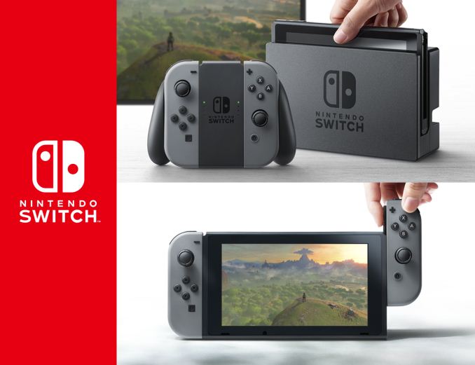
Earlier today Nintendo took the wraps off of their next generation console, Switch. Formerly known by the codename NX, the Switch is the successor to both Nintendo’s portable DS and set top Wii console lines, utilizing a portable, tablet-like unit that can be docked to behave like a set top console. Today’s announcement, in the form of a 3 minute trailer, is meant to tease the console ahead of its full launch in March of 2017.
While I’ll skip the commentary on the console’s unusual design – dedicated gaming sites can offer better context – I wanted to dive into the hardware in the Switch. Given that this was a teaser, I was not expecting a reveal of any of the hardware specifications of the console, and indeed neither Nintendo’s teaser video nor their related press release made any mention of the underlying hardware. However shortly after the reveal went live, NVIDIA sent out an email to the press and posted a blog of their own. As it turns out, while today is still just a teaser, in some ways we’re already getting more information about the console than in any previous generation of Nintendo’s hardware.
In their blog post, NVIDIA confirmed that they would be providing the underlying SoC for the console. As this is still ultimately a teaser, NVIDIA’s own details are light, but their announcement confirms that it’s a custom version of their Tegra SoC. Curiously, no mention of the CPU core in that SoC is mentioned. However as it’s a Tegra, something ARM-based is the logical (if not only) choice. And on the GPU side, as you’d expect, they’re using a GPU based on one of NVIDIA’s existing GPU architectures, though the company isn’t specifying if it’s Pascal or Maxwell (I’d assume Pascal, but consoles are known for their long development cycles).
Otherwise, as far as specifications go that’s all we get for now. Though as NVIDIA is supplying a whole SoC there are obviously many more parts to the package that we’ll hopefully learn about in the near future. More CPU and GPU details are obviously the most interesting aspect – does the Switch SoC use Denver CPU cores? – but there’s also the matter of memory bandwidth, WiFi support, and the many other functional blocks that make up an SoC.
For NVIDIA, this is the first console hardware win for the company since the PlayStation 3, which launched in 2006. In the set top console market, AMD has since provided the GPU (and often, the CPU) for the most recent generation of consoles. Otherwise NVIDIA has never had a 3rd party portable console win, primarily because both Nintendo and Sony developed their respective SoCs internally for the 3DS and Vita.
In fact, given that Nintendo previously did much of their portable console development work internally, this is a notable shift for how the company operates. The 3DS was essentially a custom SoC combining multiple ARM11 (ARMv6) CPU cores with an OpenGL ES 1.1 generation GPU from the little-known Digital Media Professionals (DMP). So this is the first time Nintendo has contracted out their SoC needs to a third party in such a visible fashion. I’m actually a bit surprised that NVIDIA is even allowed to talk about their involvement at this point in time, given Nintendo’s historical focus on secrecy.
Though all of this also helps to underline just how big a jump in technology the Switch is from the 3DS. On the CPU side alone it’s reasonable to assume we’re looking at CPU design in the neighborhood of 4.x DMIPS/MHz, versus ARM11’s approximate 1.3 DIMPS/MHz rate, so IPC will have increased significantly, never mind an increase in frequency. Meanwhile on the GPU side, Nintendo is going from a GPU that didn’t even have a programmable GPU pipeline (i.e. shaders) to a fully modern GPU, essentially catching up on a decade of mobile GPU development in a single bound. Given that the console has to work as both the company’s portable and set top consoles, Nintendo has opted to use far more modern tech than their traditionally conservative designs.

Finally, without reading too much into a 5 paragraph announcement, there is one other interesting nugget of information in NVIDIA’s blog post that further shows just how deep the NVIDIA/Nintendo relationship is going here. Along with providing the SoC, NVIDIA also has a major stake in the development of the console’s API and middleware. While NVIDIA presumably isn’t developing the entire software stack, they make special note of the fact that they are providing a new “lightweight” API, NVN, for the console. NVIDIA is also providing middleware in the form of “a revamped physics engine, new libraries, advanced game tools and libraries” and “custom software for audio effects and rendering” which sounds a great deal like NVIDIA having brought over major parts of their GameWorks SDK, including the PhysX physics simulation libraries and VRWorks Audio library.
In any case, it will be interesting to see how this plays out over the next few months. The mobile world has changed significantly since the 3DS was launched in 2011, something that the Switch’s design makes obvious. Nintendo has gone in a very different direction than either their console rivals or the smartphone market that is always threatening to encroach on mobile consoles, and that’s reflected in both the unusual dual-mode console and the hardware inside of it.


109 Comments
View All Comments
khanikun - Tuesday, October 25, 2016 - link
Someone's never heard of wireless controllers for PC or Android tablets.KoolAidMan1 - Saturday, October 22, 2016 - link
No, this solves their biggest problem which is splitting development resources between mobile and handheld game development while giving a future path for both platforms at once.Their mobile business is still MASSIVE, bigger than Playstation 4 and XBox One combined. People totally forget about this.
All Nintendo development will be on one platform instead of split between two. Mario, Zelda, Splatoon, Pokemon, Fire Emblem, Monster Hunter, all on one platform. It perfectly leverages Nintendo's strengths while giving them a competitive moat against the other platforms.
dragonsqrrl - Thursday, October 20, 2016 - link
I'm very interested to learn more about the hardware specs. I kind of figured it would be a custom SOC, as Parker's TDP is too high, its CPU block seemingly too complex, and it integrates a lot of unnecessary automotive oriented features. Alternatively the X1 would be approaching 2 years old by the time Switch launches.Hopefully it's Pascal based.
barleyguy - Thursday, October 20, 2016 - link
NVidia said in their blog post that it's "the same architecture found in the highest performing graphics cards." To me that means it's definitely Pascal.I'm thinking it's a custom version of the Tegra X2.
Cygni - Thursday, October 20, 2016 - link
Given the notoriously bad battery life of the Tegra K1 based Shield Tablet (which this really seems to just be a rewrapped and updated version of), a full X2 may suck too much juice to be considered here, even with its die shrink compared to K1. A cut down X2 may be what we are talking about here.Yojimbo - Thursday, October 20, 2016 - link
There is no X2. That's just what people chose to call a Pascal-based spiritual successor to the X1. So talking about a full or cut-down X2 doesn't really make sense. But my opinion is that the Tegra used in the Switch probably has more CUDA cores than the Drive PX 2 SOC. Judging by NVIDIA's lineup of Pascal GPUs, TSMC's 16FF+ process seems to allow for high clock rates if one is willing to pay the price in terms of power, and low power if one scales back the clocks. I think the SOC probably draws significantly more power when in the dock than when operating as a mobile device.The dock may also have some sort of cooling system built into it.Cygni - Thursday, October 20, 2016 - link
Well most people are calling Parker "X2", since its very much an iterative variation of X1. Same 256 CUDA core count, same 4 A57 cores, etc. And Parker is what is in the Drive PX 2.I personally think there is no chance a chip the size and needs of Parker/X2 lands in a handheld. K1 is a much smaller chip and has terrible battery life in the Shield tablet. Even with the gains from the dieshrink and a big clock hit, thats asking a fairly huge leap in energy efficiency. Like I talked about before, a cut-down version of Parker (with, say, 192 CUDA cores, similar to K1) seems more likely to me if they have any hopes of offering reasonable gaming life.
Yojimbo - Thursday, October 20, 2016 - link
Ignoring cost, die size isn't the biggest consideration, but rather power. Power efficiency is exactly the advantage TSMC's 16FF+ has over their 20SoC. I'm guessing the X1 is smaller than the K1, but the X1 uses more power with the extra cores because 20SoC's main advantage over their 28nm processes is areal density.From TSMC's website:
"TSMC's 20nm process technology can provide 30 percent higher speed, 1.9 times the density, or 25 percent less power than its 28nm technology."
and
"TSMC's 16FF+ (FinFET Plus) technology can provide above 65 percent higher speed, around 2 times the density, or 70 percent less power than its 28HPM technology. Comparing with 20SoC technology, 16FF+ provides extra 40% higher speed and 60% power saving."
Now the English isn't easy to interpret and those numbers don't completely jibe. Maybe things changed over time. But the overall picture is surely accurate. 16FF+ barely provides any density improvement over 20SoC. But 16FF+ provides large power savings over 20SoC whereas 20SoC provides small power savings over 28nm.
Now for the Shield Tablet. The Shield Tablet has an 8 inch 1920x1200 display. The Switch will most likely have a display with significantly fewer pixels. In addition, displays today should be more efficient than when the Shield Tablet came out. The Switch display should be consuming much less power than the Shield Tablet display, and the Tegra inside the Switch will be driving far fewer pixels than the one inside the Shield Tablet.
When calling the Shield Tablet inefficient you are comparing its SoC to other SoCs driving high density displays, but at much lower performances. Look at the following chart:
http://images.anandtech.com/graphs/graph8329/66084...
It shows that limiting the Shield Tablet to 30 FPS gives it good battery life in GFXBench 3.0 compared to other phablets and tablets. Now look as its relative onscreen and offscreen performance numbers:
http://images.anandtech.com/graphs/graph8296/65868...
http://images.anandtech.com/graphs/graph8296/65867...
The Shield Tablet has better GPU-intensive battery life than those other devices even when it's running constantly at a frame rate that's significantly higher than the average frame rate any of those other devices can achieve. The Shield Tablet has a 6% larger battery and a lower resolution screen than the Tab S 8.4, but I don't think that explain a 29% longer battery life when maintaining a frame rate the Tab S 8.4 can't maintain even in an offscreen test.
The Tegra SoCs get a bogus rap for battery life. We can't easily apply the Shield Tablet's numbers to the Switch because of the display differences, but its performance/Watt compared to other SoCs seems to be good. Comparing the NVIDIA desktop chips, the Pascal-based 1070 has a 50% higher clock, 25% more cores, and a 33% lower TDP than the Kepler-based 770. Kepler is of course the GPU architecture in the Tegra K1. I wouldn't venture to guess a number of hours, but I think there is a very good chance a Pascal GPU on TSMC's 16FF+ with more than 256 CUDA cores (384?) can clock down to run a game at 720p for mobile gaming with a decent battery life and clock up to run a game at 1080p when docked. Of course, battery life is dependent on Nintendo's willingness to invest in a large battery. Note that 384 CUDA cores clocked at 1.3 GHz would give 1 TFLOPS of peak performance. Clocked down to 800 Mhz like the Tesla P4 it may be able to run at 8 W or less and run games on a 720p display. The Xbox One has 1.3 TFLOPS of peak performance, and Pascal is known to achieve higher efficiency in its architecture than GCN. Of course the Xbox One tends to render in native resolutions less than 1080p and then upscale. The tricky issue for the Tegra might be the memory bandwidth required for 1080p. Could they possibly include some eDRAM that is only switched on when docked?
Compare the specs of the P4 and the P40, both passively cooled Pascal-based cards, and you'll see the inspiration for what I am talking about. The P4 is clocked much lower and much more efficient. Certainly the DRAM is part of the story, but so is the GPU. Then compare the P4 with the M4. The M4 uses a 28nm GPU and already includes the Maxwell achitectural efficiency improvements that the K1 presumably doesn't have, being Kepler based. The M4's DRAM bandwidth is much lower than the P4's. If allowed to use more die space, within the same TDP range the P4 has over twice the theoretical peak performance of the M4. Who knows, maybe the P4 is TDP bound in lots of applications the M4 and the P40 are not, but the difference seems impressive.
psychobriggsy - Friday, October 21, 2016 - link
Thanks for your post - it enumerates my feelings too. Note that Pascal in Tegra will have double-rate FP16 which can be used for many shaders, which will boost effective performance past XB1 when docked, even if the FP32 figures are only around 1 TFLOPS (384 cores, 1.3GHz).However, it's Nintendo, so I'm really expecting 750 GFLOPS docked from the Switch, likely from 256 cores.
Yojimbo - Friday, October 21, 2016 - link
Yes, the possibility of using FP16 is a very good point. NVIDIA's blog does say "The newest API, NVN, was built specifically to bring lightweight, fast gaming to the masses." I wondered what "lightweight" is supposed to mean. Perhaps it means the use of FP16.