AMD's Future in Servers: New 7000-Series CPUs Launched and EPYC Analysis
by Ian Cutress on June 20, 2017 4:00 PM EST- Posted in
- CPUs
- AMD
- Enterprise CPUs
- EPYC
- Whitehaven
- 1P
- 2P
NUMA NUMA IEI: Infinity Fabric Bandwidths
The news about AMD using four Zeppelin dies from Ryzen to form EPYC is not new news, having been shown several times before. However, given the design of the silicon and how the cores communicate, there has been a few worries about how the intra-package communications will be affected by not being a single monolithic die. Beyond that, socket-to-socket communications can also be an issue without sufficient latency and bandwidth.
In a single monolithic die, the latency to access other cores is usually a predictable average, with a regular latency and bandwidth out to the memory channels. Because EPYC has two memory channels per die, if a core needs to access DRAM associated with another die, it adds additional hops and latency to the access, slowing down potential instruction throughput. In the land of dual socket systems, this is known as NUMA: Non-Unified Memory Architecture. The way around a NUMA environment is data locality – keeping the data that a core needs as close as feasibly possible. Solving NUMA is a difficult task, and attempted both at the silicon and software level. Most high-end professional software packages designed for dual-socket systems are NUMA aware, and are designed to compensate for this. The majority of non-high-end software though, is not.
Intra-Socket
With the quad-die design, a single EPYC processor might essentially have four zones for NUMA to occur, based on communication paths. AMD went to specifically address this issue in their design briefings.
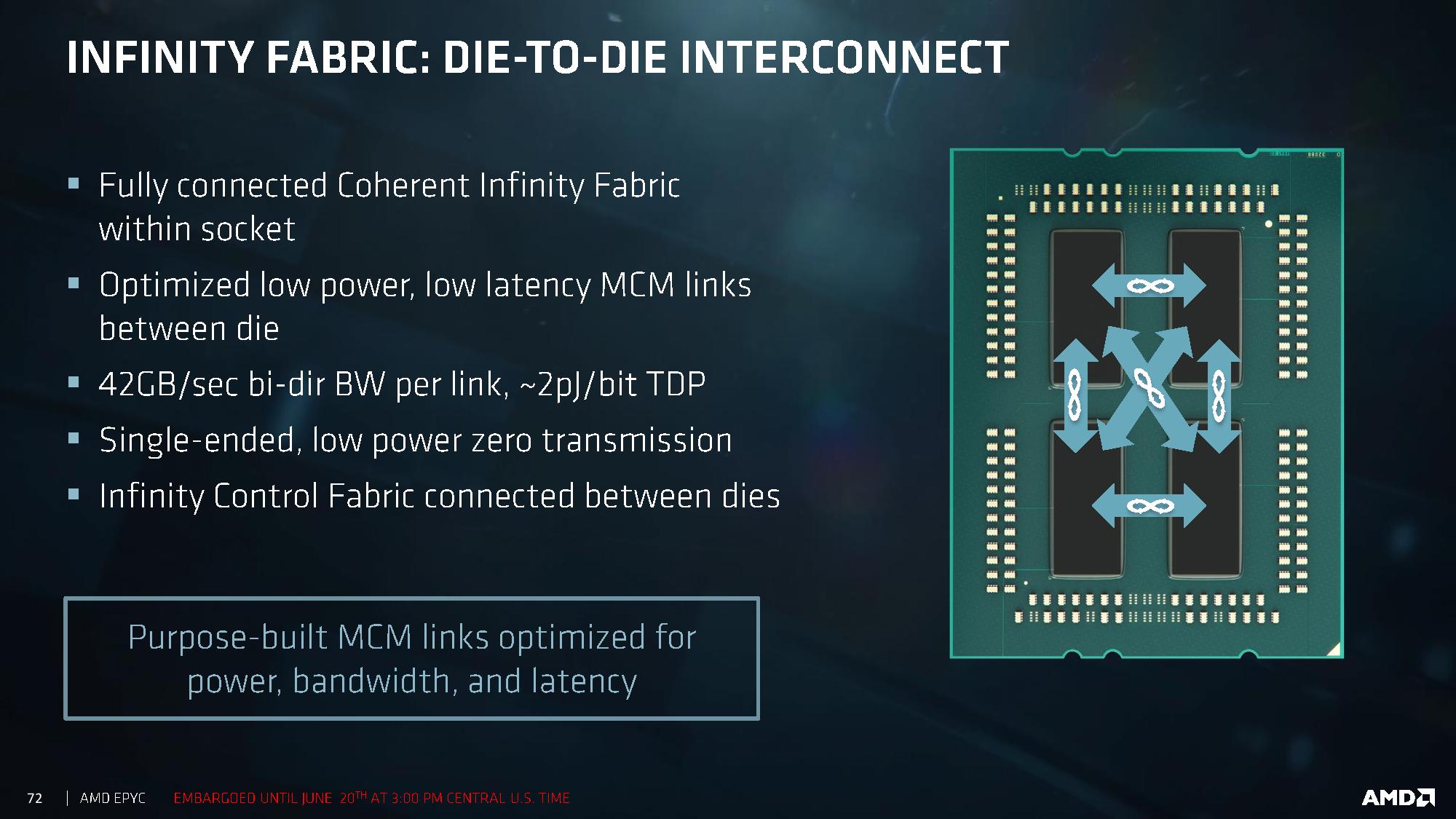
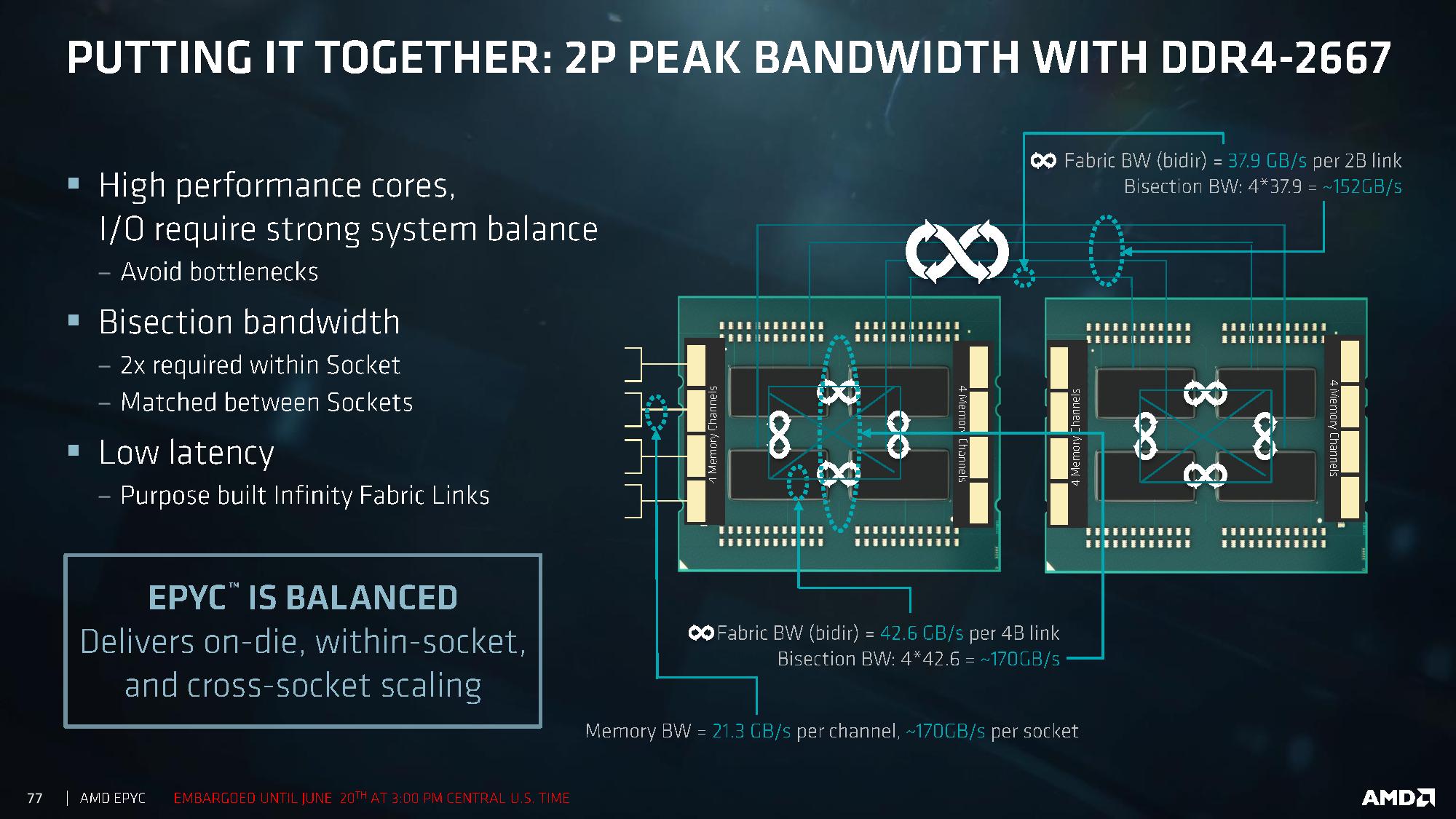
Within a single processor, each of the three dies is directly linked to each other through the Infinity Fabric, so only one hop is ever needed when data goes off-die. The connectivity here is set at a bidirectional 42.6 GB/sec per link, at around an average energy of ~2 pJ per bit (or 0.672W per link, 0.336W per die per link, totaling 4.032W for the chip). It is worth noting that Intel’s eDRAM for Broadwell was set as a 50 GB/s bidirectional link, so in essence moving off die in EPYC has a slightly slower bandwidth than Crystalwell. With a total of six links within the silicon, that provides a total of 2 terabits per second of data movement, although AMD didn’t state what the bottlenecks or latency values were.
Inter-Socket
Socket-to-socket communication is designed at the die level, rather than going through a singular interface. One die in each processor is linked to the same die in the other processor, meaning that for the worst-case scenario data has to make two hops to reach a core or memory controller on the other side of the system. Each link has a bidirectional 37.9 GB/s bandwidth, which is only slightly less than the intra-socket communication bandwidth, although we would expect socket-to-socket to have a slightly higher latency based on distance. AMD has not shared latency numbers at this time.
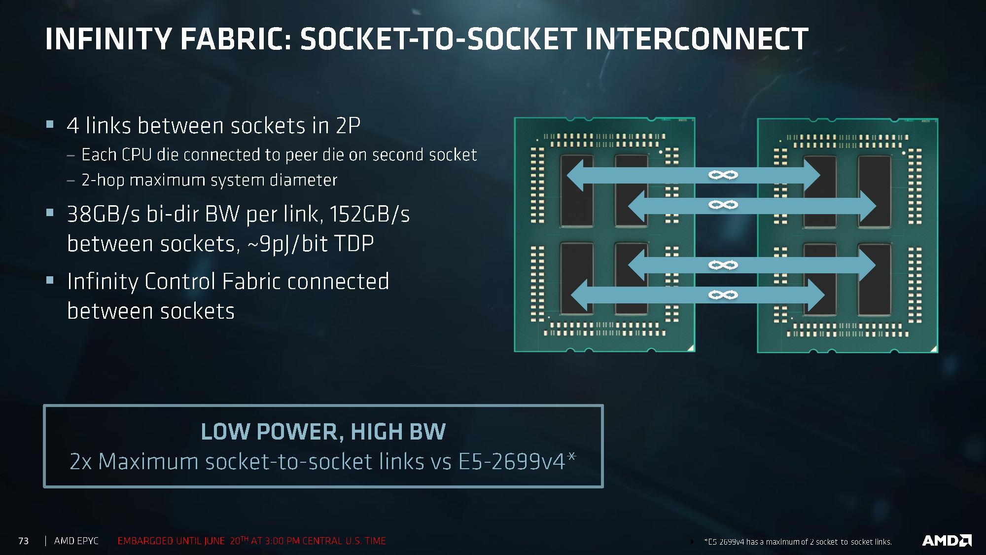
At 37.9 GB/s per link, this totals 152 GB/s between sockets, which AMD states runs at an average of 9 pJ per bit. So at full speed, this link will consume 10.94W between the two sockets, or 5.48W per processor and 1.368W per silicon die.
Totaling the 1.368W per die for socket-to-socket plus 3*0.336W per die for intra-socket communications, the Infinity Fabric can consume 2.376W per silicon die on average when going at full speed.
Infinity Fabric Latency
AMD has not provided Infinity Fabric numbers for latency. We are waiting on information, but this is likely going to be a critical answer for some software packages. Based on testing done by PC Perspective, we already know some latency numbers within a single Zeppelin die from the Ryzen platform. This allows us to fill in the following table showing how long it takes to ping another core:
| EPYC (Naples) Thread Ping Connections | ||
| Latency | Bandwidth | |
| Within A Core | 26 ns | - |
| Core-to-Core, Same CCX | 42 ns | - |
| Core-to-Core, Different CCX, Same Die | 142 ns | - |
| Die-to-Die, Same Package | ? | 42.6 GB/s |
| Die-to-Die, Different Socket, One Hop | ? | 37.9 GB/s |
| Die-to-Die, Different Socket, Two Hops | ? | 37.9 GB/s |
| Core to DRAM, Same Die | ? | 42.6 GB/s |
| Core to DRAM, Different Die | ? | 42.6 GB/s |
| Core to DRAM, Different Socket, One Hop | ? | 37.9 GB/s |
| Core to DRAM, Different Socket, Two Hops | ? | 37.9 GB/s |
PCIe Bandwidth
Each Zeppelin die can create two PCIe 3.0 x16 links, which means a full EPYC processor is capable of eight x16 links totaling the 128 PCIe lanes presented earlier. AMD has designed these links such that they can support both PCIe at 8 GT/s and Infinity Fabric at 10.6 GT/s, although in PCIe mode this means 32GB/s of bidirectional bandwidth per link, suitable for 256GB/s per socket. One of AMD’s proposed benefits here is link bifurcation support:
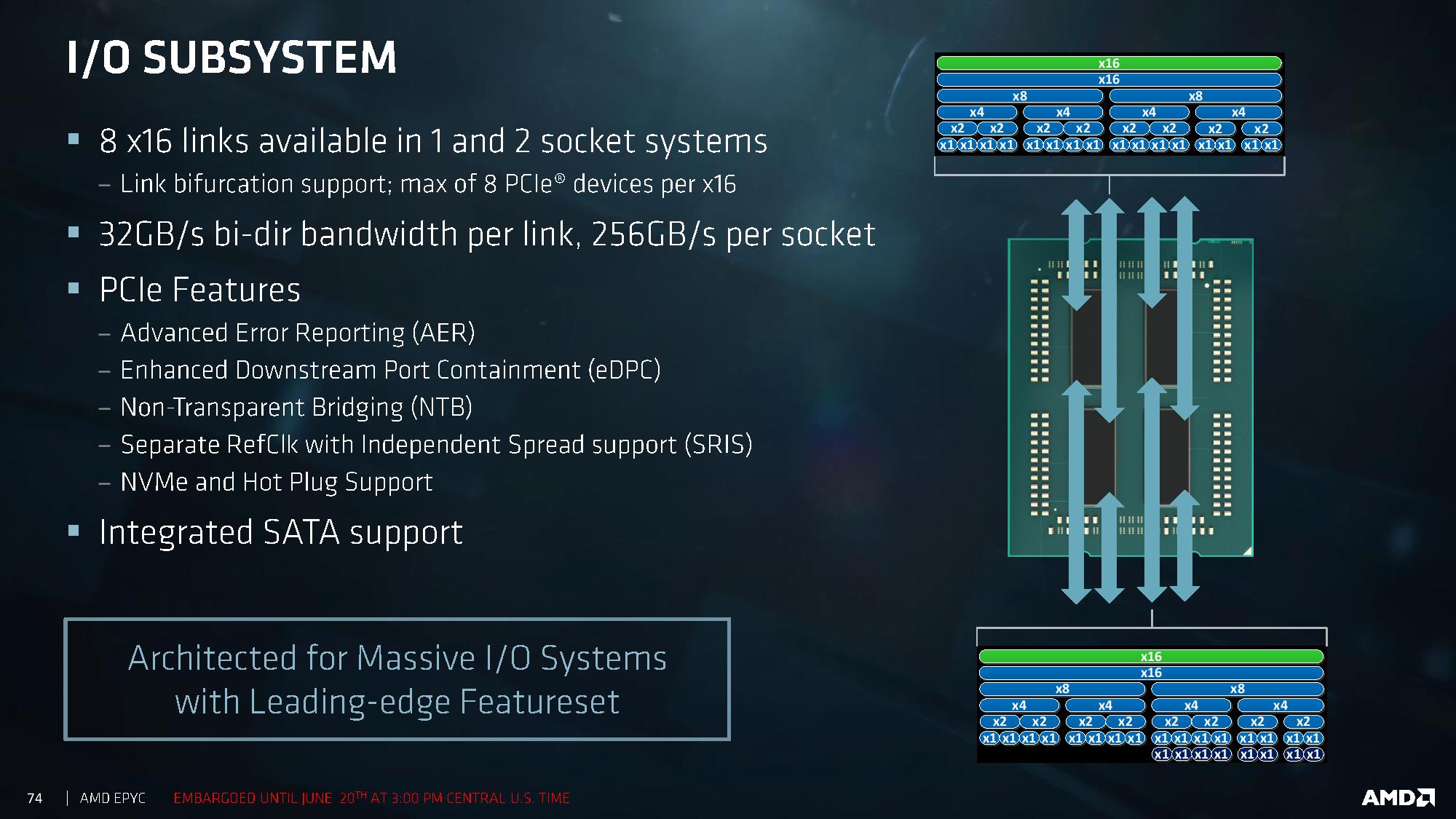
Each x16 link can support Infinity Fabric (green), PCIe (blue) and SATA (dark blue). PCIe can be bifurcated all the way down to sets of x1, although there will be a limit of 8 PCIe devices per x16 link, but this becomes a mix and match game: x8 + x4 + x2 + x1 + x1 + x1 + x1 becomes entirely valid for a single x16 link, and each CPU has eight of these such links. For the SATA connectivity, each x16 link can support 8 SATA drives as a result. If you really want 64 devices per processor, welcome to your platform without buying PCIe switches. AMD states that as an NVMe implementation, supporting 32 NVMe devices is going to be no sweat for an EPYC system.
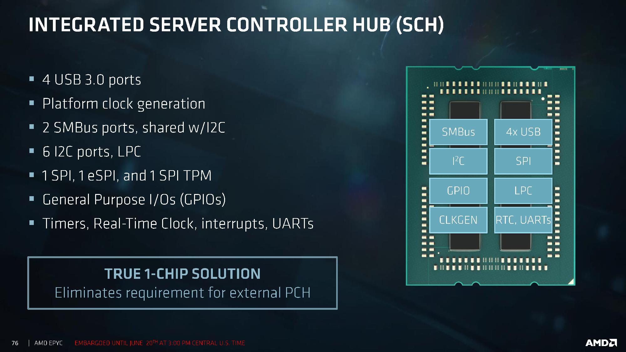
This also relates to the Sever Controller Hub, which acts as part of the design offering four USB 3.0 ports, SMBus, I2C, SPI, eSPI, TPM, GPIOs, timers and UARTs.
Combining The Bandwidth
Altogether, AMD is stating that they are relatively unconcerned about NUMA related issues, with bandwidth between dies and between sockets being relatively similar. It is worth noting that the 42.6 GB/s die-to-die bandwidth is identical to the dual-channel memory bandwidth quoted per die:
Time will tell if these become bottlenecks. Latency numbers please, I’d love to fill in that table above.


131 Comments
View All Comments
msroadkill612 - Wednesday, June 21, 2017 - link
Sounds a powerful feature for vid editors etc."Hot-swap NVMe/SAS3/SATA3
drive bays and M.2 slots"
Breit - Wednesday, June 21, 2017 - link
Really?: http://images.anandtech.com/galleries/5699/epyc_te..."All 2P E5 scores were derived from the following ICC compiler-based test results per spec.org, multiplied by 0.575 to convert them from the ICC compiler to GCC -O2 v6.1..."?!?
Not cool.
TC2 - Wednesday, June 21, 2017 - link
i smell a tragedy for amd with those "multiplications" :)HollyDOL - Wednesday, June 21, 2017 - link
Reminds me so called "Resultin's constant" joke...[Value you get] [any operator] [Resultin's constant] = [Value you wanted]
TC2 - Wednesday, June 21, 2017 - link
precisely!try another behavioural pattern: great claims, feeble results :)
to compare E5-2698 v4 20 cores with EPYC 7551 32 cores - 32/20 = 1.6, the extrapolation is claimed to be +44% or 1.44.
therefore 1.6/1.44=1.1(1).
now we can to conclude that for a 32 core xeon (it's easy for intel) the result will be +11% for intel, and no more advantage for amd at all!!!
such mathematical practices are ridiculous!
FreckledTrout - Wednesday, June 21, 2017 - link
Anyone buying these is going to want to see some large independent reviews / studies. Some of the larger companies looking at these say like Amazon's data center may get a few and do a study. I think that type of info is what everyone should wait on. These numbers look like they came from the marketing side of the house.Intel999 - Wednesday, June 21, 2017 - link
"Anyone buying these is going to want to see some large independent reviews / studies. Some of the larger companies looking at these say like Amazon's data center may get a few and do a study."Those companies that shared the stage with AMD for this presentation were included in the 5,000 Epyc chips that were given to OEMs/ODMs to test and validate over the last six months.
All the big boys know what EPYC is capable of and it seems that most are quite impressed.
Zizy - Wednesday, June 21, 2017 - link
Yeah well the story is that they obtained GCC 6.1 scores (by benching the CPU) for the top CPU and found out those are ~40% lower than the official ones. Some of that is ICC cheating on tests, some of that is optimization level.So, they reduced all official scores by the same ~40% for this comparison (with the top part being actually benched and achieved that result as on slides).
I can't fault them for using the middle ground GCC for those benchmarks, and the normalization step is reasonable enough as well. The only real issue here is use of -O2 instead of more optimized code. Sure, Ryzen/Epyc is new and GCC likely cannot optimize as good for it (which is probably they reason they used default O2), but this is not a valid excuse, should have used O3 at least if not advanced flags.
petteyg359 - Thursday, June 22, 2017 - link
Don't be a ricer. -O3 is often else than -O2 and EVERYBODY with a clue recommend against using it anywhere, ever.Zan Lynx - Monday, June 26, 2017 - link
Erm. I use GCC with -O3 in a library I build at my job. With profile feedback it is easily 20% faster than -O2. So I don't know where these "clue" people are. I've only been coding for 20 years or so. I may not have a clue yet.