GlobalFoundries Details 7 nm Plans: Three Generations, 700 mm², HVM in 2018
by Anton Shilov on June 23, 2017 12:00 PM EST- Posted in
- Semiconductors
- GlobalFoundries
- EUV
- 7nm
- DUV
- 7LP
Keeping an eye on the ever-evolving world of silicon lithography, GlobalFoundries has recently disclosed additional details about its 7 nm generation of process technologies. As announced last September, the company is going to have multiple generations of 7 nm FinFET fabrication processes, including those using EUV. GlobalFoundries now tells us that its 7LP (7 nm leading performance) technology will extend to three generations and will enable its customers to build chips that are up to 700 mm² in size. Manufacturing of the first chips using their 7LP fabrication process will ramp up in the second half of 2018.
| GlobalFoundries 7LP Platform | |||||
| 7nm Gen 1 | 7nm Gen 2 | 7nm Gen 3 | |||
| Lithography | DUV | DUV + EUV | DUV + EUV | ||
| Key Features | Increased performance, lower power, higher transistor density vs. 14LPP. | Increased yields and lower cycle times. | Performance, power and area refinements. | ||
| Reasons for EUV insertion | - | To reduce usage of quadruple and triple patterning. | To improve line-edge roughness, resolution, CD uniformity, etc. | ||
| HVM Start | 2H 2018 | 2019 (?) | 2020 (?) | ||
7 nm DUV
First and foremost, GlobalFoundries reiterated their specs of their first-gen 7 nm process, which involves deep ultraviolet (DUV) lithography with argon fluoride (ArF) excimer lasers operating on a 193 nm wavelength. The company’s 7 nm fabrication process is projected to bring over a 40% frequency potential over the 14LPP manufacturing technology that GlobalFoundries uses today, assuming the same transistor count and power. The tech will also reduce the power consumption of ICs by 60% at the same frequency and complexity.
For their newest node, the company is focusing on two ways to reduce power consumption of the chips: implementing superior gate control, and reducing voltages. To that end, chips made using GlobalFoundries' 7LP technology will support 0.65 – 1 V, which is lower than ICs produced using the company’s 14LPP fabrication process today. In addition, 7LP semiconductors will feature numerous work-functions for gate control.
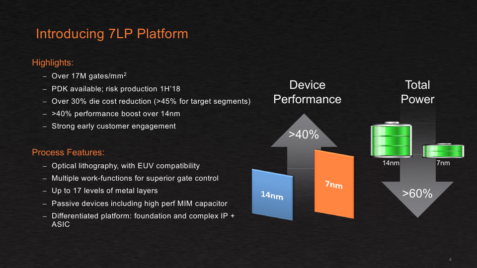
When it comes to costs and scaling, the gains from 7LP are expected to be a bit atypical from the usual manufacturing process node advancement. On the one hand, the 7 nm DUV will enable over 50% scaling over 14LPP, which is not something surprising given the fact that the latter uses 20 nm BEOL interconnections. However, since 7 nm DUV involves more layers that require triple and quadruple patterning, according to the foundry the actual die cost reduction will be in the range between 30% and 45% depending on application.
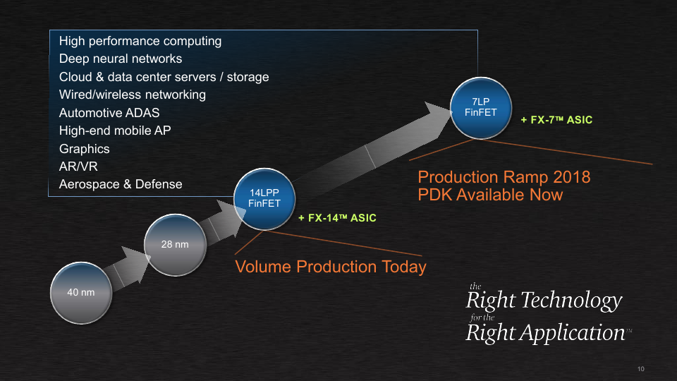
The 7 nm platform of GlobalFoundries is called 7LP for a reason — the company is targeting primarily high-performance applications, not just SoCs for smartphones, which contrasts to TSMC’s approach to 7 nm. GlobalFoundries intends to produce a variety of chips using the tech, including CPUs for high-performance computing, GPUs, mobile SoCs, chips for aerospace and defense, as well as automotive applications. That said, in addition to improved transistor density (up to 17 million gates per mm2 for mainstream designs) and frequency potential, GlobalFoundries also expects to increase the maximum die size of 7LP chips to approximately 700 mm², up from the roughly 650 mm² limit for ICs the company is producing today. In fact, when it comes to the maximum die sizes of chips, there are certain tools-related limitations.
| Advertised PPA Improvements of New Process Technologies Data announced by companies during conference calls, press briefings and in press releases |
|||||
| GlobalFoundries | |||||
| 7nm Gen 1 vs 14LPP |
7nm Gen 2 vs Gen 1 |
7nm Gen 3 vs Gen 1/2 |
|||
| Power | >60% | same* | lower | ||
| Performance | >40% | same* | higher | ||
| Area Reduction | >50% | none | yes | ||
| *Better yields could enable fabless designers of semiconductors to bin chips for extra performance or lower power. | |||||
GlobalFoundries has been processing test wafers using 7 nm process technology for clients for several quarters now. The company’s customers are already working on chips that will be made using 7 nm DUV process technology, and the company intends to start risk production of such ICs early in 2018. Right now, the clients are using the 0.5 version of GlobalFoundries' 7 nm process design kit (PDK), and later this year the foundry will release PDK v. 0.9, which will be nearly final version of the kit. Keep in mind that large customers of GlobalFoundries (such as AMD) do not need the final version of the PDK to start development of their CPUs or GPUs for a given node, hence, when GF talks about plans to commercialize its 7LP manufacturing process, it means primarily early adopters — large fabless suppliers of semiconductors.
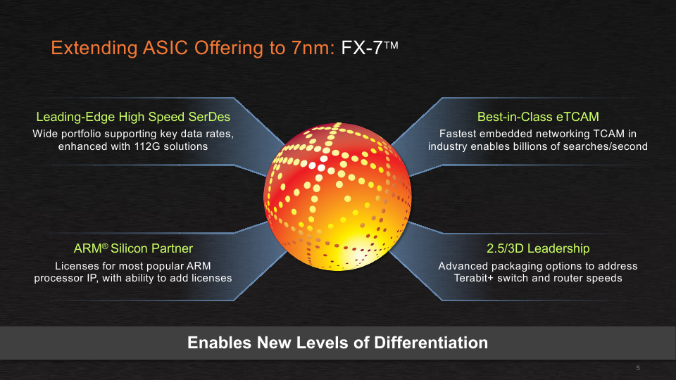
In addition to its PDKs, GlobalFoundries has a wide portfolio of licenses for ARM CPU IP, high-speed SerDes (including 112G), and 2.5D/3D packaging options for its 7LP platform. When it comes to large customers, GlobalFoundries is ready for commercial production of chips using its 7 nm DUV fabrication process in 2018.
Fab 8 Ready for 7LP, Getting Ready for EUV
Speaking of high volume manufacturing using their 7LP DUV process, it is necessary to note that earlier this year GlobalFoundries announced plans to increase the production capacity of their Fab 8. Right now, the output of Fab 8 is around 60,000 wafer starts per month (WSPM), and the company expects to increase it by 20% for 14LPP process technology after the enhancements are complete.
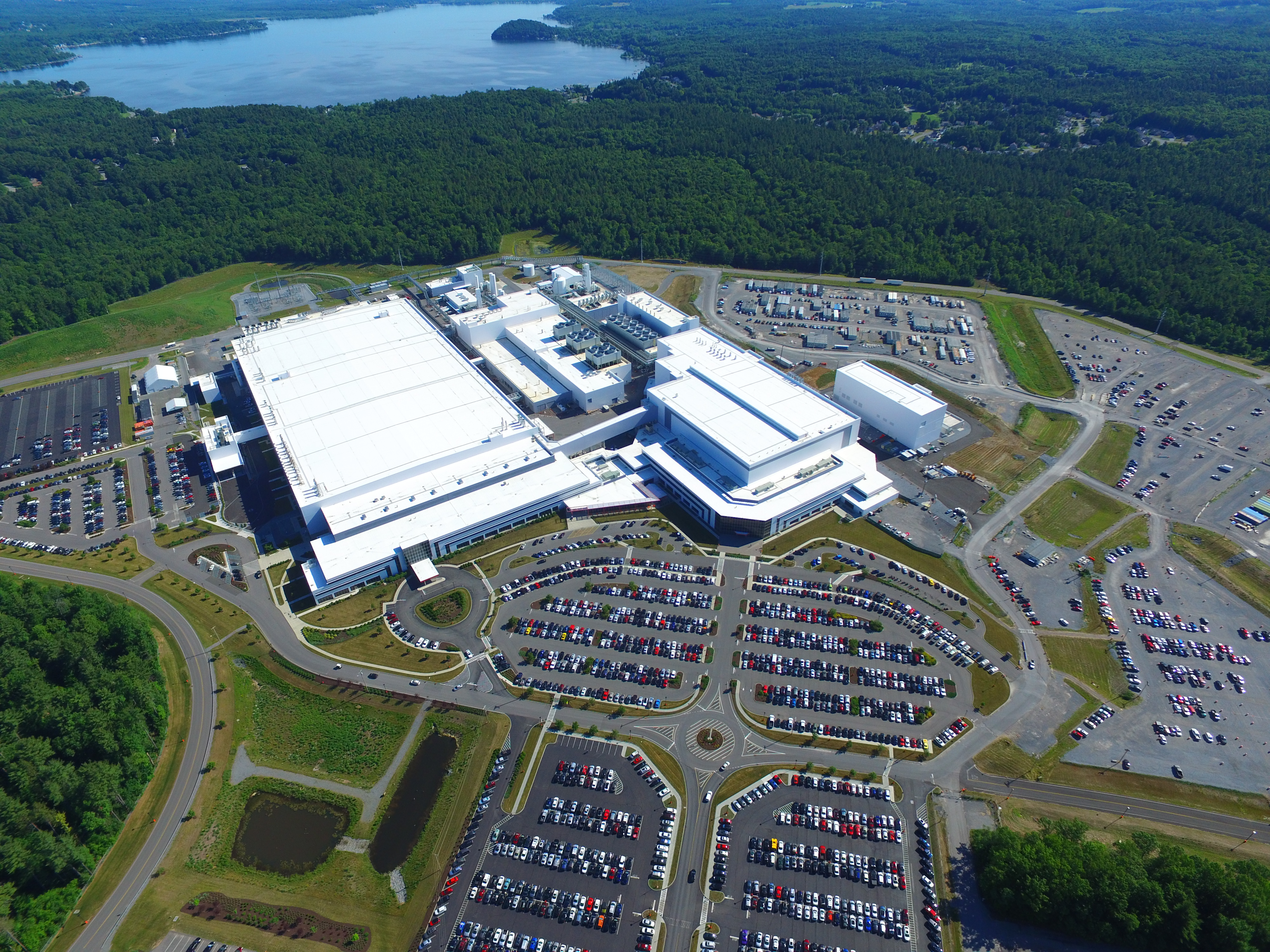
The expansion does not involve physical enhancement of the building, which may indicate that the company intends to install more advanced scanners with increased output capabilities. GlobalFoundries naturally does not disclose details about the equipment it uses, but newer scanners with higher output and better overlay and focus performance will also play their role in HVM using 7 nm DUV that relies on quadruple patterning for select layers.
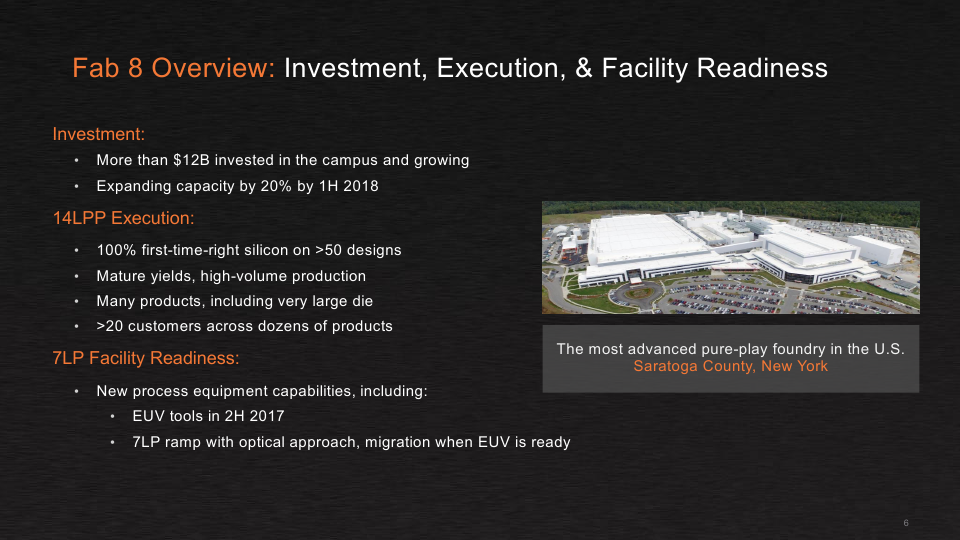
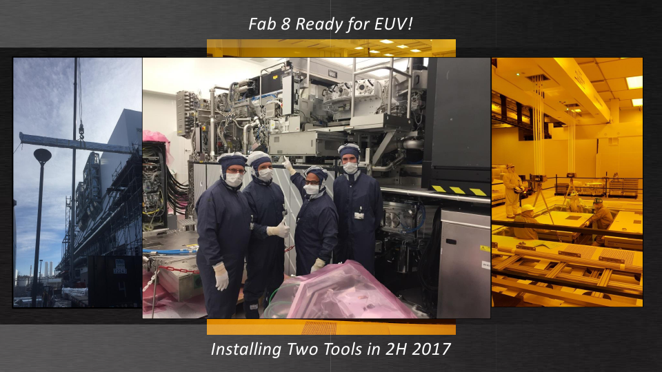
In addition to more advanced ASML TWINSCAN NXT DUV equipment, GlobalFoundries plans to install two TWNSCAN NXE EUV scanners into the Fab 8 in the second half of this year. This is actually a big deal because current-generation fabs were not built with EUV tools in mind. Meanwhile, EUV equipment takes up more space than DUV equipment because of the light source and other aspects.
EUV: Many Problems Solved, But Concerns Remain
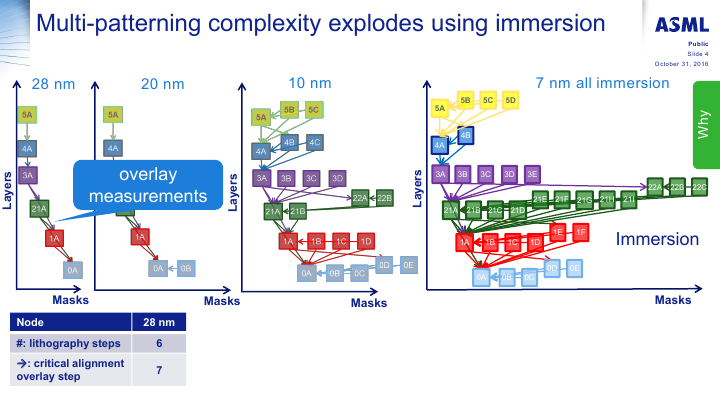
Usage of multi patterning for ultra-thin process technologies is one of the reason why the industry needs lithography that uses extreme ultraviolet wavelength of 13.5 nm. As avid readers know, the industry has been struggling to develop EUV tools suitable for HVM, and while significant progress has been made recently, EUV is still not quite up to scale. This is exactly why GlobalFoundries is taking a cautious approach to EUV that involves multiple generations. Keep in mind that GlobalFoundries does not seem to have official names for different iterations of its 7 nm process technologies. The only thing that the company is talking about now is its “7LP platform with EUV compatibility.” Therefore, all our generations-related musings here are just for a better understanding of what to expect.

ASML has developed several generations of EUV scanners and has demonstrated light sources with 205 W of power. The latest TWINSCAN NXE scanners with recent upgrades have demonstrated an availability that exceeds 60%, which is good enough to start their deployment, according to GlobalFoundries. Eventually, availability is expected to increase to 90%, in line with DUV tools.
Meanwhile, there are still concerns about protective pellicles (films) for EUV photomasks, mask defects, as well as EUV resists. On the one hand, current pellicles can handle productivity rates of up to 85 wafers per hour (WpH), which is well below 125 WpH planned for this year. Basically, this means that existing pellicles cannot handle powerful light sources required for HVM. Any defect on a pellicle can affect wafers and dramatically lower yields. Intel demonstrated pelliclized photomasks that could sustain over 200 wafer exposures, but we do not know when such pellicles are expected to enter mass production. On the other hand, powerful light sources are required for satisfactory line-edge roughness (LER) and local critical dimensions (CD) uniformity primarily because of imperfections of resists.
7 nm EUV Gen 1: Improving Yields, Reducing Cycles
Given all the EUV-related concerns, GlobalFoundries will start to insert EUV for select layers in a bid to reduce the usage of multi patterning (and eliminate quadruple patterning in general, if possible), thereby improving yields. At this time the company is not disclosing when it plans to start using EUV tools for manufacturing, only stating that they'll do so “when it is ready.” It is unlikely that EUV will be ready in 2018, so it is logical to expect the company to use EUV tools no sooner than 2019.
Such approach makes a lot of sense because it enables GlobalFoundries to increase yields for its customers and to learn more about what it will take to get EUV ready for HVM. In the best-case scenario, GlobalFoundries will be able to produce designs developed for 7 nm DUV with multi patterning using its 7 nm EUV tech. However, one should keep in mind two factors. First, semiconductor developers release new products every year. Second, GlobalFoundries will begin to insert EUV tools into production at least a couple of quarters after the launch of the first 7 nm DUV chips. Therefore, it is highly likely that the first EUV-based chips produced at GlobalFoundries will be new designs rather than chips originally fabbed on the all-DUV process.
7 nm EUV Gen 2: Higher Transistor Density and Line-Edge Roughness
Depending how fast the industry addresses the current EUV challenges related to masks, pellicles, CD uniformity, LER and other things, GlobalFoundries will eventually roll out another generation of its 7 nm EUV process.
The second-gen 7 nm EUV manufacturing technology from GlobalFoundries will feature improved LER and a better resolution, which the company hopes will enable higher transistor densities with lower power and/or higher performance. Though given the experimental nature of the tech behind this process, as you'd expect GlobalFoundries is not saying when certain problems are to be resolved and when it can offer appropriate services to its customers.
Finally, 3rd Gen 7LP will likely introduce some new design rules to enable geometry scaling and/or higher frequencies/lower power, but in general I'm expecting that the transition to this process should be relatively seamless to IC designers. After all, the majority of layers will still use DUV. The only question is whether GlobalFoundries will need to install additional TWINSCAN NXE scanners into the Fab 8 for its 2nd Gen 7 nm EUV process technologies, which would also indicate that the number of layers processed using EUV had increased.
5 nm EUV: Adjustable Gate-All-Around FETs
A week before GlobalFoundries disclosed their 7LP platform plans, IBM and their Research Alliance partners (GlobalFoundries and Samsung) demonstrated a wafer processed using a 5 nm manufacturing process. ICs on the wafer were built using silicon nanosheet transistors (aka gate-all-around FETs [GAA FETs]) and it looks like they will be building blocks for semiconductors in the future. The big question of course is when.
![]()
GAA FETs developed by IBM, GlobalFoundries, and Samsung stack silicon nanosheets in such a way that every transistor now has four gates. The key thing about GAA FETs is that the width of nanosheets can be adjusted within a single manufacturing process or even within the IC design to fine-tune performance or power consumption. When it comes to performance/power/area(PPA)-related improvements, IBM claims that when compared to a 10 nm manufacturing process, the 5 nm technology offers 40% performance improvement at the same power and complexity, or 75% power savings at the same frequency and complexity. However keep in mind that while IBM participates in the Alliance, announcements by IBM do not reflect the actual process technologies developed by GlobalFoundries or Samsung.
![]()
IBM, GlobalFoundries, and Samsung claim that adjustments to GAA FETs were made using EUV, which is logical as the three companies use an ASML TWINSCAN NXE scanner at the SUNY Polytechnic Institute's NanoTech Complex (in Albany, NY) for their R&D work. Technically, it is possible to produce GAA FETs using DUV equipment (assuming that it is possible to get the right CD, LER, cycle times, etc.), but it remains to be seen how significantly the 5 nm process and designs will rely on EUV tools.
| Industry FinFET Lithography Roadmap, HVM Start Data announced by companies during conference calls, press briefings and in press releases |
||||||||||||
| 2016 | 2017 | 2018 | 2019 | 2020 | 2021 | |||||||
| 1H | 2H | 1H | 2H | 1H | 2H | 1H | 2H | |||||
| GlobalFoundries | 14LPP | 7nm DUV | 7nm with EUV* | 5nm (?) | ||||||||
| Intel | 14 nm 14 nm+ |
14 nm++ 10 nm |
10 nm+ 10 nm++ |
|||||||||
| Samsung | 14LPP 14LPC |
10LPE | 10LPP | 8LPP 10LPU |
7LPP | 6 nm* (?) | ||||||
| SMIC | 28 nm** | 14 nm in development | ||||||||||
| TSMC | CLN16FF+ CLN16FFC | CLN10FF CLN16FFC |
CLN7FF CLN12FFC |
CLN12FFC/ CLN12ULP |
CLN7FF+ | 5 nm* (?) | ||||||
| UMC | 28 nm** | 14nm | no data | |||||||||
| *Exact timing not announced **Planar |
||||||||||||
Neither of the three members of the Research Alliance talked about timeframe of 5 nm HVM, but a wild guess would put 5 nm EUV in 2021 (if not later).
![]()
Some Thoughts
Wrapping things up, based on recent announcements it's looking increasingly likely that EUV will in fact make it out of the lab and intro high volume production. In just the past couple of weeks GlobalFoundries and two of its development partners have made several announcements regarding EUV in general, increasingly calling it a part of their future. This does not mean that they do not have a Plan B with multi patterning, but it looks like EUV is now a part of the mid-term future, not the long-term one. Still, it's telling that no one is giving a deadline for EUV beyond “when it is ready.”
Just like GlobalFoundries said before (like other foundries), the insertion of EUV equipment into their manufacturing flow would be gradual. The company plans to install two scanners this year to use them for mass production several quarters down the road, but GlobalFoundries has not made any further announcements beyond that. Ultimately while the future for EUV is looking brighter, the technology is still not ready for prime time, and for the moment no one knows quite when it'll finally meet all of the necessary metrics for volume production.
Finally, speaking of the 7LP platform in general, it is interesting that GlobalFoundries will be primarily targeting high-performance applications with the new technology, and not mobile SoCs like some other contract fabs. This despite the fact that the 7LP platform supports ultra-low voltages (0.65 V) and should be able to address mobile applications. So from a performance/power/area point of view, while the 7LP manufacturing process looks rather competitive, it remains to be seen just how GlobalFoundries’ partners will use the capabilities of the new process.
Related Reading:


76 Comments
View All Comments
turtile - Saturday, June 24, 2017 - link
Adding more cores will require redesigning the architecture in order to work with current motherboards. Each 8 core complex has it's own dual memory controller. So it you keep adding more 8 core complexes, you need more memory slots. They could make 12 core complexes but it would lower the bandwidth from the memory and require more work.jjj - Friday, June 23, 2017 - link
Samsung has provided more details that that, there is a 5nm and 4nm , with 4nm using GAA.TSMC has their 7nm HPC and the version targeting outo,not just what you list.
And ofc there is FD-SOI for both GF and Samsung and that one is relevant enough in consumer- lower end mobile, image sensors, IoT.
Banykrk - Friday, June 23, 2017 - link
-on TMSC roadmap -> not CLN12ULP but CLN22ULP and this was official, yes 22nm planar-TSMC 7FF+ is EUV and this is also official information
-in GF 22nm SOI ULP and ULL and 14nm SOI is missing
I included only logic nodes
Frenetic Pony - Friday, June 23, 2017 - link
Next year should be great for upgrading your current laptop. Both AMD (which will have Zen2 based mobile parts) and Intel will be putting out new nodes. Some quick math shows current 15 watt parts could squeeze into sub tablet space. And CoreY like parts could fit into (larger) phone like form factors!Imagine a Windows phone ditching the "Phone" OS part and just running full Windows. Or a decent gaming laptop fitting into a modern "ultrabook" like form factor. Hell yeah.
Hurr Durr - Saturday, June 24, 2017 - link
Eh, I wish it was that rosy. Realistically, new nodes will first need to be optimized on desktop, so we`re likely two years away from gaming notebooks in our pockets. I`d much rather have a new phone anyway, Lumia 730 is nice as a daily driver, but certainly shows its age.TheinsanegamerN - Saturday, June 24, 2017 - link
Perhaps. It depends if AMD grows a backbone and demands OEMs make decent machines. I've had a lenovo L440 for years. I wanted a kaveri powered machine, and then a carrizo machine. All I could fine were cheap 15 inch machines with single channel memory and cheap casings.AMD making a great chip is half the battle. Wrangling OEMs in and making them behave is another battle entirely, one AMD has refused to fight thus far.
Meteor2 - Sunday, June 25, 2017 - link
It's always amused me that it took Microsoft to show hardware companies how to produce quality. It's like they'd given up. Shame Microsoft has too; perhaps they think 'job done, back to our core'.Intel's Ultrabook was a fine initiative also. AMD needs something similar but they also can't spread themselves too thinly.
mapesdhs - Tuesday, June 27, 2017 - link
Funny thing about MS, their OSs drive me nuts, but I'm usually impressed with their peripheral tech. Went hunting for a wifi mouse with a good range, the MS basic model worked the best by miles.KAlmquist - Friday, June 23, 2017 - link
One way to go from a 14nm process to a 7nm process is to cut the feature size in half, which would reduce the area by a factor of 4. The Global Foundaries is promising an area reduction of a factor of 2, which suggests that GF has doubled the marketing hype.If this is true, it is good news for the development of semiconductor technology going forward. We are facing physical limits on how small features can be made on silicon based semiconductors. It may be physically impossible to develop a 1nm process on silicon using feature size reduction alone. But if GF is able to double the amount of marketing hype each generation, it will be able to hit 1 nm in six generations without reducing feature size AT ALL.
I expect that there are limits to what marketing hype can achieve. Ultimately, marketing is limited by the gullibility of the public. But Moore's law, which predicts a doubling of density every two years, has had a good 40 year run, and it's not clear we've hit the end yet. If increased marketing hype has anything close to as good a run as increased density, we can look to see advances in marketing hype driving semiconductor technology for many years into the future.
SaturnusDK - Friday, June 23, 2017 - link
I think it shows remarkable good business sense on the part of GloFo to realize that trying to develop a 10nm production process, investing in manufacturing facilities for that, and having to run it until it has at least repaid the costs involved in that would not make sense for their customers, primarily AMD, when just stretching the 14nm process a bit further would enable them (AMD) to leapfrog a process node ahead their competition (Intel).The brilliance is the staged development and realizing what can be done now, and what can be done later. Accepting that yields and profits might be a bit lower with current DUV technology and then improving both as EUV evolves. And note that GloFo focus on performance. The 7nm process is squarely intended for performance products like AMD CPUs and GPUs compared to the low power 7nm process, primarily for ARM SoCs, that Samsung and TSMC plans to implement first.
That means that Intel will only have about 6 month or maybe less process lead with Cannonlake before AMD will leapfrog them and overtake the process lead. And it doesn't seem like Intel has any concrete plans for implementing 7nm any time soon.
It's difficult to see this in any other way than this spells big trouble for Intel going ahead. One of their biggest selling points have always been a process lead that allowed their chips to be clocked higher and therefore have a greater single core performance because the IPC gains will be minuscule going forward.