The Intel Core i9-7980XE and Core i9-7960X CPU Review Part 1: Workstation
by Ian Cutress on September 25, 2017 3:01 AM ESTExplaining the Jump to Using HCC Silicon
When Intel makes its enterprise processors, it has historically produced three silicon designs:
- LCC: Low Core Count
- HCC: High Core Count (sometimes called MCC)
- XCC: Extreme Core Count (sometimes called HCC, to confuse)
The idea is that moving from LCC to XCC, the silicon will contain more cores (sometimes more features), and it becomes cost effective to have three different designs rather than one big one and disable parts to meet the range. The size of the LCC silicon is significantly smaller than the XCC silicon, allowing Intel to extract a better production cost per silicon die.
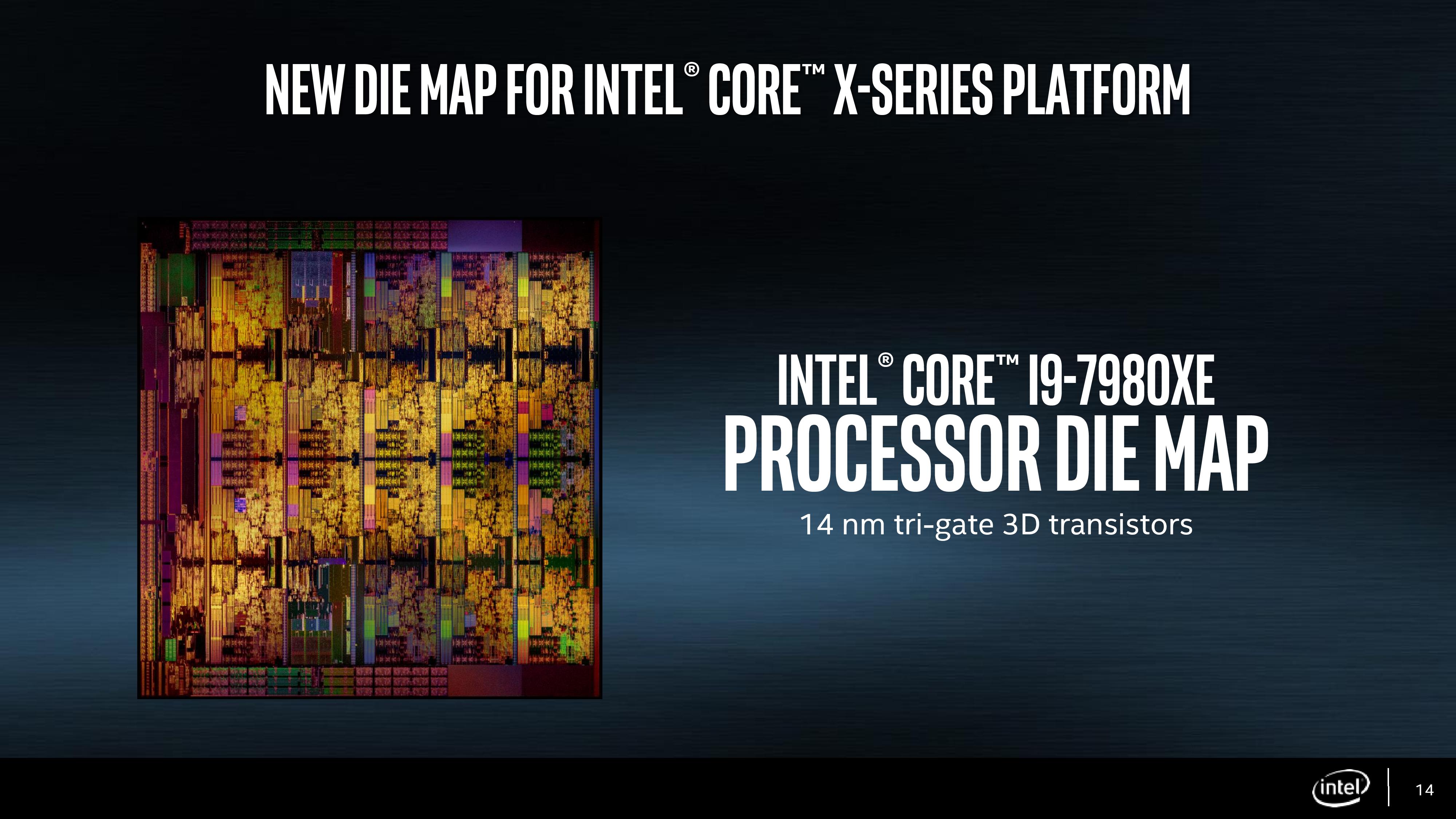
| Skylake-SP Die Sizes (from chip-architect.com) | |||
| Arrangement | Dimensions (mm) |
Die Area (mm2) |
|
| LCC | 3x4 (10-core) | 14.3 x 22.4 | 322 mm2 |
| HCC | 4x5 (18-core) | 21.6 x 22.4 | 484 mm2 |
| XCC | 5x6 (28-core) | 21.6 x 32.3 | 698 mm2 |
In the enterprise space, Intel has each of the three designs throughout its Xeon processor stack, ranging from four-core parts (usually cut down versions of the LCC silicon) all the way up to 28 core parts (using XCC) for this generation. The enterprise platform has more memory channels, support for error correcting and high-density memory, the ability to communicate to multiple processors, and several other RAS (reliability, accessibility, serviceability) features that are prominent for these markets. These are typically disabled for the prosumer platform.
In the past, Intel has only translated the LCC silicon into the prosumer platform. This was driven for a number of reasons.
- Cost: if users needed XCC, they had to pay the extra and Intel would not lose high-end sales.
- Software: Enterprise software is highly optimized for the core count, and systems are built especially for the customer. Prosumer software has to work on all platforms, and is typically not so multi-threaded.
- Performance: Large, multi-core silicon often runs at a low frequency to compensate. This can be suitable for an enterprise environment, but a prosumer environment requires responsiveness and users expect a good interactive experience.
- Platform Integration: Some large silicon might have additional design rules above and beyond the smaller silicon support, typically with power or features. In order to support this, a prosumer platform would require additional engineering/cost or lose flexibility.
So what changed at Intel in order to bring HCC silicon to the HEDT prosumer platform?
The short and shrift answer that many point to is AMD. This year AMD launched its own high-end desktop platform, based on its Ryzen Threadripper processors. With their new high performance core, putting up to 16 of them in a processor for $999 was somewhat unexpected, especially with the processor beating Intel’s top prosumer processors in some (not all) of the key industry benchmarks. The cynical might suggest that Intel had to move to the HCC strategy in order to stay at the top, even if their best processor will cost twice that of AMD.
Of course, transitioning a processor from the enterprise stack to the prosumer platform is not an overnight process, and many analysts have noted that it is likely that Intel has considered this option for several generations: testing it internally at least and looking at the market to decide when (or if) it is a good time to do so. The same analysts point to Intel’s initial lack of specifications aside from core count when these processors were first announced several months ago: specifications that would have historically been narrowed down at that point in previous designs if they were in the original plans. It is likely that the feasibly of introducing the HCC silicon was already in process, but actually moving that silicon to retail was a late addition to counter a threat to Intel’s top spot. That being said, to say Intel had never considered it would perhaps be a jump too far.
The question now becomes if the four areas listed above would all be suitable for prosumers and HEDT users:
- Cost: Moving the 18-core part into the $1999 is unprecedented for a consumer processor, so it will be interesting to see what the uptake will be. This does cut into Intel’s professional product line, where the equivalent processor is nearer $3500, but there are enough ‘cuts’ on the prosumer part for Intel to justify the difference: memory channels (4 vs 6), multi-processor support (1 vs 4), and ECC/RDIMM support (no vs yes). What the consumer platform does get in kind is overclocking support, which the enterprise platform does not.
- Software: Intel introduced its concept of ‘mega-tasking’ with the last generation HEDT platform, designed to encompass users and prosumers that use multiple software packages at once: encoding, streaming, content creation, emulation etc. Its argument now is that even if software cannot fully scale beyond a few cores, a user can either run multiple instances or several different software packages simultaneously without any slow-down. So the solution to this is rather a redefinition of the problem rather than anything else, which could have applied previously as well.
- Performance: Unlike enterprise processors, Intel is pushing the frequency on the new HCC parts for consumers. This translates into a slightly lower base frequency but a much higher turbo frequency, along with support for Turbo Max. In essence, software that requires responsiveness can still take advantage of the high frequency turbo modes, as long as the software is running solo. The disadvantage is going to be in power consumption, which is a topic later in the review.
- Platform Integration: Intel ‘solved’ this by creating one consumer platform suitable for nine processors with three different designs (Kaby Lake-X, Skylake-X LCC and Skylake-X HCC). Both the Kaby Lake-X and Skylake-X parts have different power delivery methods, support different numbers of memory channels, and different numbers of PCIe lanes / IO. When this was first announced, there was substantial commentary that this was making the platform overly complex, and would lead to confusion (it lead to at least one broken processor in our testing).
Each of these areas has either been marked as solved, or redefined out of being issue (even if a user agrees with the redefinition or not).


152 Comments
View All Comments
Krysto - Monday, September 25, 2017 - link
Yes, it's total bullshit that they are misinterpreting what TDP is. I imagine this is how they'll get away with claiming a lower TDP than the real one in the 8700k chip, too, which has low base clock speed, but the super-high Turbo-Boost, which probably means the REAL TDP will go through the rough when that Turbo Boost is maximized.This is how Intel will get to claim that its chips are still faster than AMD "at the same TDP" (wink wink, nudge nudge).
Demigod79 - Monday, September 25, 2017 - link
"What a load of ignorance. Intel tdp is *average* power at *base* clocks, uses more power at all core turbo clocks here. Disable turbo if that's too much power for you."I find it ironic that you would call someone ignorant, then reveal your own ignorance about the TDP and turbo clocks.
Spunjji - Monday, September 25, 2017 - link
It is now, it wasn't before. Wanna bet on how many people noticed?SodaAnt - Monday, September 25, 2017 - link
I'm quite curious what happens if your system cooling simply can't handle it. I suspect if you designed a cooling solution which only supported 165W the CPU would simply throttle itself, but I'm curious by how much.ZeDestructor - Monday, September 25, 2017 - link
Strictly speaking, all forms of Turbo boost are a form of vendor-sanctioned overclocking. The fact that measured power goes beyond TDP when at max all-core turbo should really not be all that surprising. The ~36% increase in power for ~31% increase in clocks is pretty reasonable and inline when you keep that in mind. Especially when you factor that there has to have been a bit of extra voltage added for stability reasons (power scales linearly with clocks and current, and quadratically to exponentially with voltage).Demigod79 - Monday, September 25, 2017 - link
I agree. Everything looked good until that page. 190 watts is unacceptable, and Intel needs to correct this right away - either make the CPU run within the TDP limit, or update the TDP to 190 watts in the specs.HStewart - Monday, September 25, 2017 - link
It funny that people complain about CPU watts but never about external GPU watts. Keep in mind the GPU is smaller amount of area.artk2219 - Monday, September 25, 2017 - link
They most certainly do, that is one of the biggest gripes against Vega 64, people do seem to have short memory on how high GPU TDP's used to be however.IGTrading - Tuesday, September 26, 2017 - link
On a video card, the same manufacturer takes responsibility for the GPU, cooling system, design, PCB, components and warranty.On the CPU, you have somebody else designing the cooling system, the motherboard, the power lines and they all have to offer warranty for their components while Intel is only concerned with the CPU.
If the CPU is throttling or burnt out, they will say "sufficient cooling was not provided" and so on ...
It is a whole lot different.
whatevs - Tuesday, September 26, 2017 - link
Thermal throttling is not a burn out and not a warranty event, you don't get to warranty your gpu when it throttles under load, cooling warranty does not include cpu/gpu chip performance andIntel designed the ATX specification and the electrical specification for the boards.
You clearly don't know the things you're talking about.