Cadence Announces Tensilica Vision Q6 DSP
by Andrei Frumusanu on April 11, 2018 10:45 AM EST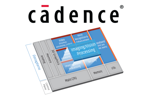
As the industry and underlying technology is evolving, we’ve seen a large shift in image processing on mobile devices, which over the last couple of years have been increasingly relying on processing to improve camera capabilities. DSPs are becoming ever more important in smartphone devices and mainstream players such as Qualcomm have touted the advantages for a long time. We’ve seen vendors such as Google even go as far as including dedicated SoCs such as the Pixel Visual Core, with the goal of augmenting the imaging processing capabilities of their devices.
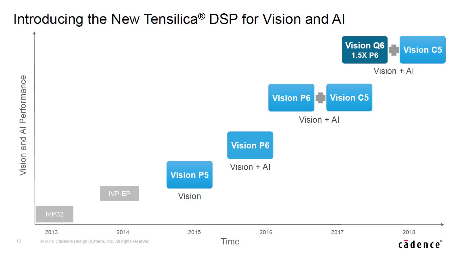
Today’s announcement comes from Cadence, whom is unveiling their new DSP IP called theTensilica Vision Q6. The Q6 succeeds the Vision P6, which as of late has had quite a success: the P6 is included in HiSilicon Kirin 970 SoC which powers the Mate 10 and P20 devices, and serves as the main imaging processing unit enabling a wide variety of features. Cadence was also able to confirm that the IP core which serves as the “APU” for AI processing on the MediaTek P60 is also the Vision P6, which replaced the P5 from previous generation MediaTek SoCs.
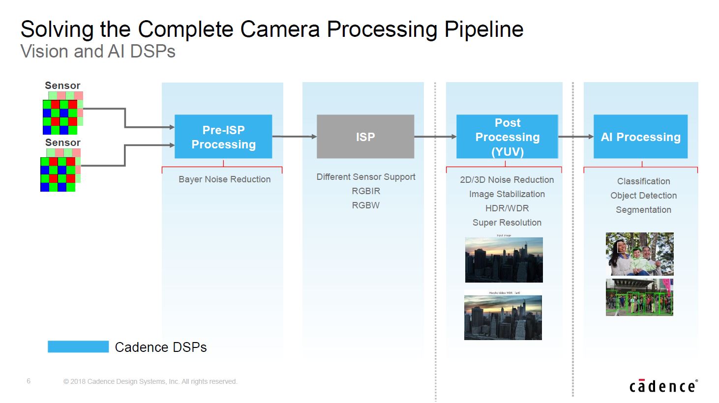
DSPs are extremely versatile in the image processing pipeline and Cadence showcases a variety of example use-cases such as noise reduction, image stabilization, HDR processing and “super resolution” scaling functionalities. The Vision P6 and Q6 also can be used for AI processing, which as noted is how MediaTek promotes capabilities of the P60.
 [ [ Huawei 20 Pro ]
I think the biggest and most impressive showcase of DSP capabilities the Vision P6 is Huawei’s extensive usage in the P20s. Here Huawei’s new camera setup with a 40MP shooter foregoes a mechanical image stabilisation mechanism for a software one which runs on the Vision P6 DSP. The killer feature on the P20s is the new improved “Night”-mode shooting capability which is able to do software image stacking and stabilisation, resulting in to date unprecedented extreme low-light captures. The P20 Pro’s hybrid zoom functionality through the 2 or 3 cameras also makes extensive usage of the DSP. I’ll be covering the P20’s cameras in more detail in the upcoming review.
As an aside for anyone wondering, the new IP is the Q because Q succeeds P in the alphabet, and Cadence wanted to differentiate the new architecture that way.
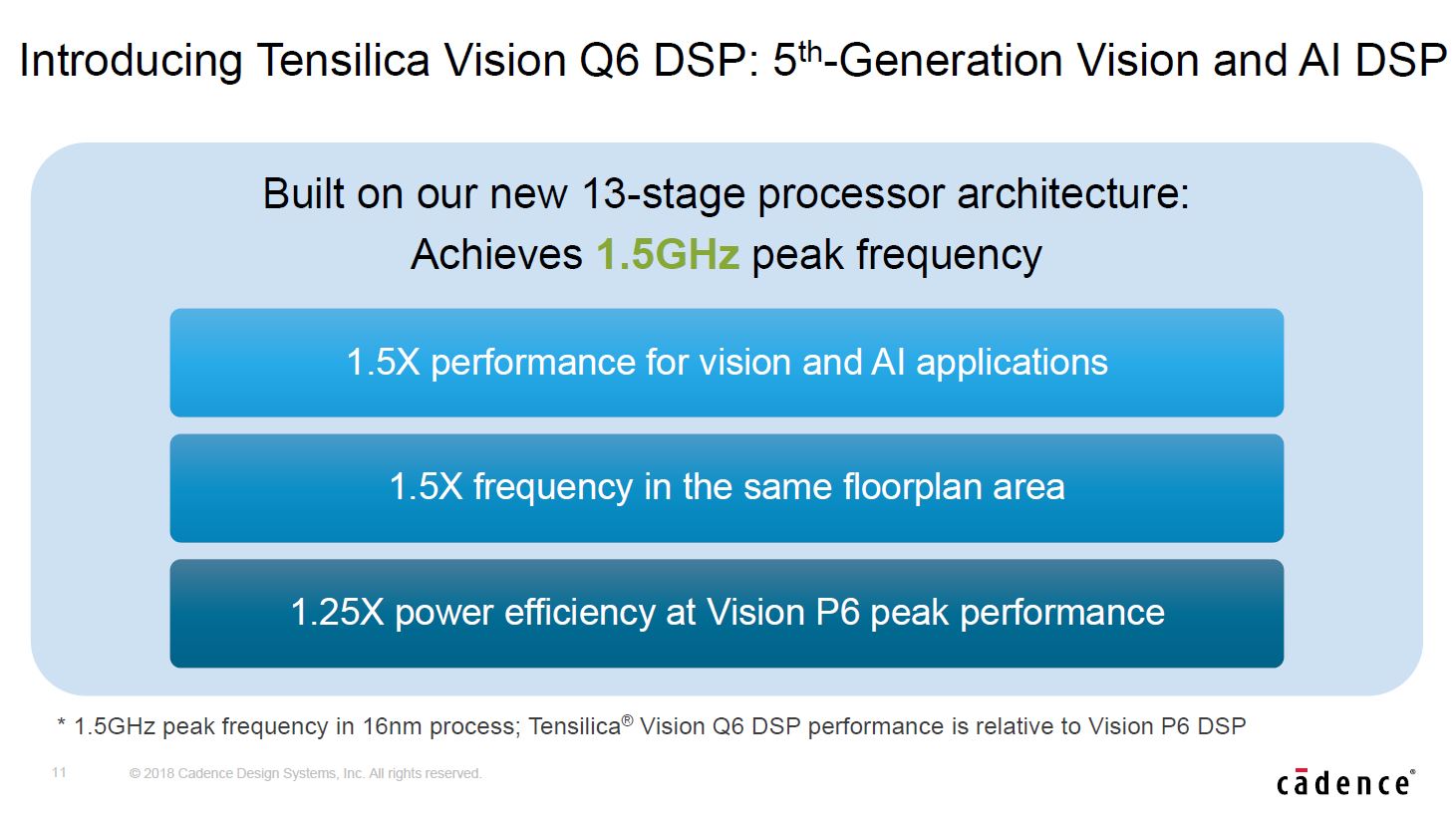
The main characteristics of the Q6 is a 1.5x improvement in performance, which is enabled through a 1.5x increase in frequency. This frequency increase was achieved through the increase of the pipeline depth of the microarchitecture from 10 stages to 13 stages. The Q6 also improves the micro-architectural power efficiency by 25% when compared at iso-performance levels to the P6. Naturally the Q6 goes further in performance so it does mean that peak power will be higher and efficiency might be lower at that point. I asked what kind of figure we’re talking about here, and according to Cadence we’re looking at around 150mW for typical use-cases on a 16nm process – which is far lower than I had expected and certainly there’s a lot of power headroom there.
Increasing performance is possible through integration of more DSPs – here the silicon vendor can just throw in more Q6s onto the SoC, similar to how MediaTek uses 2 P6s on the P60. It’s also possible to mix-and-match configurations with for example multiple Q6s for image processing and then one or more C5’s for increased machine learning inferencing performance.
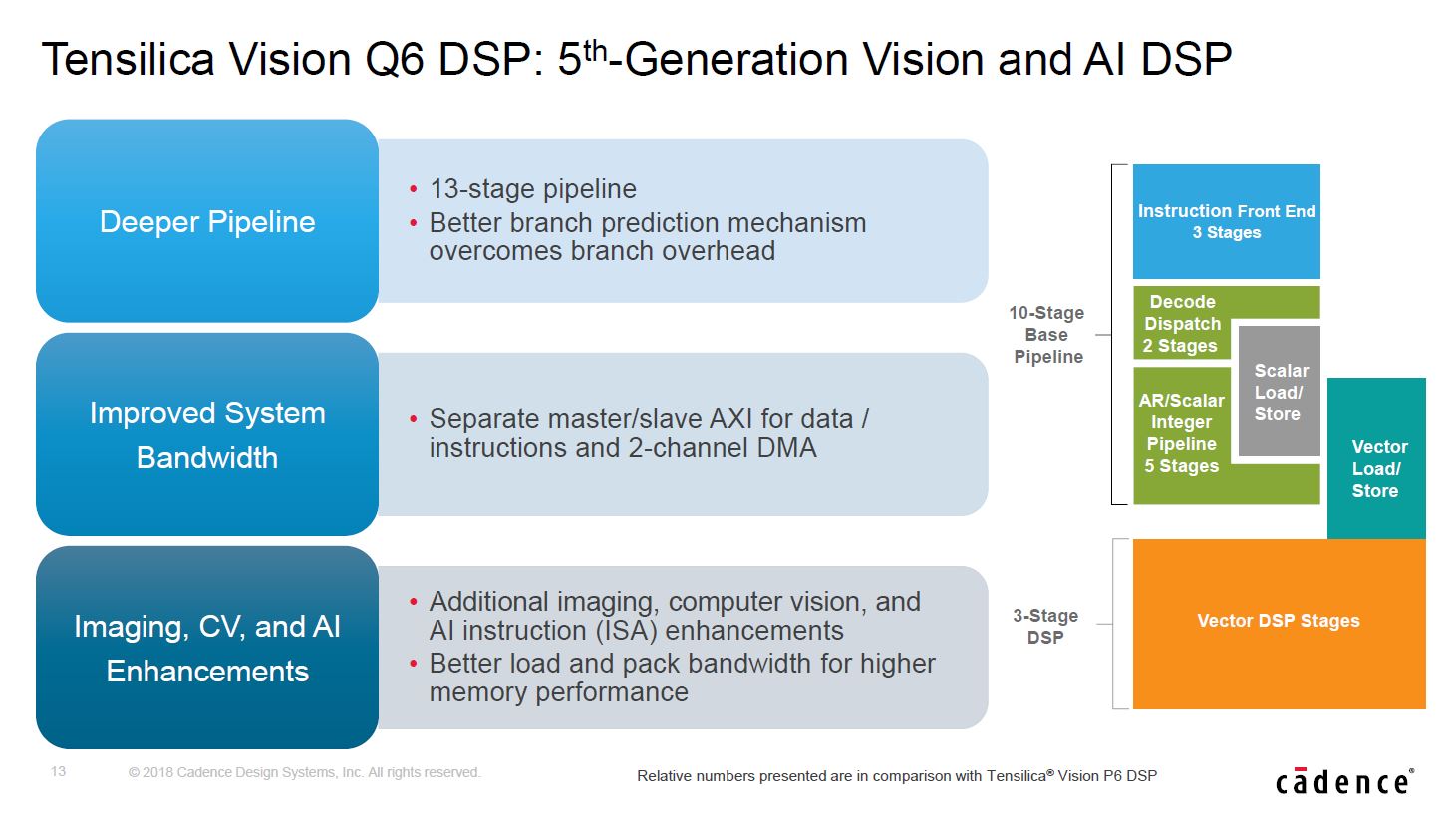
The micro-architectural improvements circle around the big pipeline depth changes. Cadence was able to improve the branch prediction such that the deeper pipeline depth doesn’t negatively affect IPC. Among other improvements were memory system enhancements both on the interconnect side as well as on the core side, with improved load/store units which enable higher bandwidth. We’ve also seen improvements in the ISA with new instructions for image processing and machine learning which enhance performance up to 2x on various imaging kernels (Clock frequency performance increase included).
The Q6 seems to maintain the other high-level capabilities of the P6, such as its SIMD capabilities of 4 vector ops per cycle, each 64-way SIMD. In total the P6 and Q6 are capable of 256 ALU ops per cycle. The Q6 maintains the optional VFPU configuration option of the P6, which adds in a 32-way SIMD vector FPU with either 16-way FP32 or 32-way FP16 capabilities.
An important thing to note about the Q6 is that it maintains software compatibility with the P6, and as such vendors are able to greatly reduce their software development investments / reuse previous implementations on the new hardware.
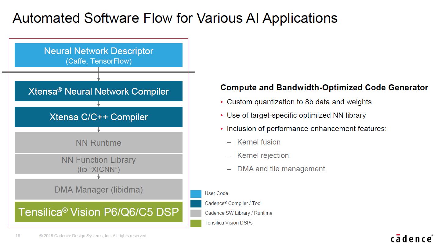
On the software side Cadence is also introducing some new features. We now see the introduction of official Android NN API support. The software platform also includes support for TensorFlow and TensorFlow Lite alongside the existing Caffee framework support. An interesting feature of the Xtensa Neural Network Compiler is the ability to allow for customized layers – something vendors might be interested in tweaking for their specialized inferencing models, which the compiler then takes care of and also does quantization into 8bit models.
Huawei and Cadence definitely raised the bar in terms of innovative features and software processing in the P20 and just shows that if the processing hardware is available, vendors will find great new uses for it. I’m expecting the mobile industry to continue down this path and I’m eager to see what will be possible.
The Vision Q6 is already being integrated into products by lead customers and is now also available for broad licensing.


20 Comments
View All Comments
Andrei Frumusanu - Wednesday, April 11, 2018 - link
The S9 doesn't seem to have a working SNPE backend/ Master Lu isn't running correctly and falling back to the CPU, that's why I didn't cover it.The plan is to test them yes, but currently the available benchmarks... are lacking.
jjj - Wednesday, April 11, 2018 - link
Thanks.I know it's messy, it always is in the early days but marketing is starting to focus on AI and we need to know what's what.
Wardrive86 - Wednesday, April 11, 2018 - link
Thanks for the article! Hope to see more companies discuss their DSPs in detailWardrive86 - Wednesday, April 11, 2018 - link
Sorry for the double post. Can a developer have access to the DSP via OpenCL, Renderscript, OpenGLES, or Vulkan?ZolaIII - Wednesday, April 11, 2018 - link
No they use their own lo level API's from Kronos.https://image.slidesharecdn.com/13embeddedvisional...
jjj - Wednesday, April 11, 2018 - link
In theory this can apply effects to video in real time , wonder if mitigating rolling shutter issues is something folks might try to address.serendip - Wednesday, April 11, 2018 - link
Does Qualcomm have something similar with their Hexagon DSPs? I imagine it wouldn't be hard to add a neural network block in there, the main issue is if it's accessible to the user.SydneyBlue120d - Thursday, April 12, 2018 - link
Yes, they have:https://semiaccurate.com/2017/12/18/qualcomms-ai-u...
tuxRoller - Thursday, April 12, 2018 - link
This isn't a vliw design? That's an interesting way to go for a dsp.Tom Womack - Tuesday, April 17, 2018 - link
Cadence is, famously, a manufacturer of EDA software.Are the ranges of IP blocks produced by EDA companies generally tied in to their EDA software, or can you use a Tensilica DSP and a Synopsys ARC processor in a design which you are compiling using Mentor tools?