TSMC: First 7nm EUV Chips Taped Out, 5nm Risk Production in Q2 2019
by Anton Shilov on October 9, 2018 4:00 PM EST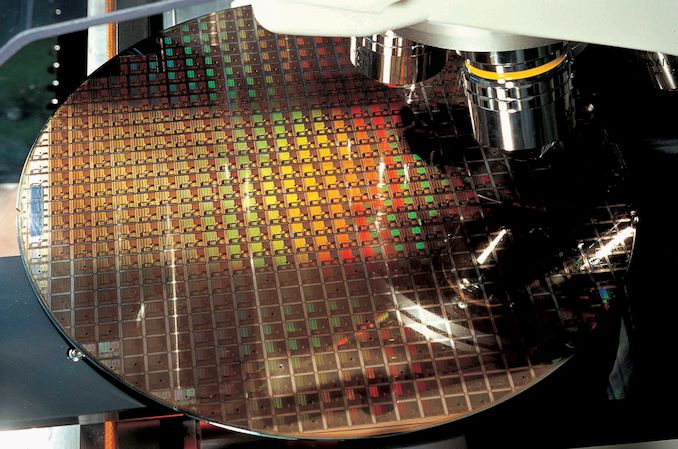
Last week, TSMC made two important announcements concerning its progress with extreme ultraviolet lithography (EUVL). First up, the company has successfully taped out its first customer chip using its second-generation 7 nm process technology, which incorporates limited EUVL usage. Secondly, TSMC disclosed plans to start risk production of 5 nm devices in April.
First 7 nm EUV Chip Tapes Out at TSMC
TSMC initiated high-volume manufacturing of chips using its first generation 7 nm fabrication process (CLN7FF, N7) in April. N7 is based around deep ultraviolet (DUV) lithography with ArF excimer lasers. By contrast, TSMC’s second-generation 7 nm manufacturing technology (CLN7FF+, N7+) will use extreme ultraviolet lithography for four non-critical layers, mostly in a bid to speed up production and learn how to use ASML’s Twinscan NXE step-and-scan systems for HVM. Factual information on the improvements from N7 to N7+ are rather limited: the new tech will offer a 20% higher transistor density (because of tighter metal pitch) and ~8% lower power consumption at the same complexity and frequency (between 6% and 12% to be more precise).
While the advantages of N7+ over its predecessors are not significant (e.g., TSMC has never mentioned performance increases that the new tech is expected to bring), it will still almost certainly be embraced wholeheartedly by developers of mobile SoCs who need to release new chips every year. That said, it is not surprising that TSMC has already taped out the first chip using its N7+ technology. Furthermore, the company is prepping a specialized version of N7 process aimed at the automotive industry, which indicates that N7/N7+ is going to be a “long” node.
TSMC is not disclosing the name of the customer whose N7+ SoC it has taped out, but considering the foundry’s alpha customers for new process technologies in the recent years, the leading suspects are obvious.
| Advertised PPA Improvements of New Process Technologies Data announced by companies during conference calls, press briefings and in press releases |
||||||||
| TSMC | ||||||||
| 16FF+ vs 20SOC |
10FF vs 16FF+ |
7FF vs 16FF+ |
7FF vs 10FF |
7FF+ vs 7FF |
5FF vs 7FF |
|||
| Power | 60% | 40% | 60% | <40% | 10% | 20% | ||
| Performance | 40% | 20% | 30% | ? | same (?) | 15% | ||
| Area Reduction | none | >50% | 70% | >37% | ~17% | 45% | ||
5 nm on Track
After N7+ comes TSMC’s first-generation 5 nm (CLN5FF, N5) process, which will use EUV on up to 14 layers. This will enable tangible improvements in terms of density, but will require TSMC to extensively use EUV equipment. When compared to TSMC’s N7, N5 technology will enable TSMC's customers to shrink area of their designs by ~45% (i.e. transistor density of N5 is ~1.8x higher than that of N7), increase frequency by 15% (at the same complexity and power) or reduce power consumption by 20% power reduction (at the same frequency and complexity).
TSMC will be ready to start risk production of chips using its N5 tech in April, 2019. Keeping in mind that it typically takes foundries and their customers about a year to get from risk production to HVM, it seems like TSMC is on-track for mass production of 5 nm chips in Q2 2020, right in time to address smartphones due in the second half of 2020.
EDA tools for the N5 node will be ready in November, so chip designs may be well underway now. But while many foundation IP blocks for N5 are ready today, there are important missing pieces, such as PCIe Gen 4 and USB 3.1 PHYs, which may not be ready until June. For some of TSMC's clients the lack of these pieces is not a problem, but many will have to wait.
One of the factors that prevents smaller companies from designing FinFET chips is development cost. Some estimates put the average cost to develop an SoC at around $150 million in labor and IP licenses. With N5 generation, these expenditures will rise to $200 – $250 million, according to EETAsia, which will limit the number of parties interested in using the tech.
Related Reading:
- TSMC Details 5 nm Process Tech: Aggressive Scaling, But Thin Power and Performance Gains
- TSMC Starts to Build Fab 18: 5 nm, Volume Production in Early 2020
- AMD's 7nm CPUs & GPUs To Be Fabbed by TSMC, on Track for 2018 - 2019
- TSMC Kicks Off Volume Production of 7nm Chips
Source: EETAsia


50 Comments
View All Comments
Samus - Wednesday, October 10, 2018 - link
Unless Intel has some amazing hat trick, like a new, unannounced, revolutionary architecture right around the corner (it isn't on the roadmaps) then they have lost microarchitecture advantage to AMD (Zen is clearly more power efficient in performance-per-watt while being more scalable) and they have lost manufacturing advantage to TSMC, who is already neck and neck with Intel and next year will surpass them on process node. Neither company accurately discloses yields but it can be assumed TSMC's are better because Intel's prices continue to go up while profit margin's remain static.Wilco1 - Wednesday, October 10, 2018 - link
"TSMC, who is already neck and neck with Intel and next year will surpass them on process node"What?!? TSMC surpassed Intel several years ago with 10nm.
Samus - Thursday, October 11, 2018 - link
>>"TSMC, who is already neck and neck with Intel and next year will surpass them on process node">What?!? TSMC surpassed Intel several years ago with 10nm.
TSMC 10nm does not equal Intel 10nm, the gate pitch is closer to Intel's 14nm.
TSMC 7nm is a smaller pitch than Intel 10nm, but both are otherwise very similar.
The process node nm doesn't mean the density of the imaged area is the same, it's simply a definition of lithography.
Wilco1 - Thursday, October 11, 2018 - link
TSMC 16nm is slightly less dense than Intel 14nm as you would expect. TSMC 10nm is without a doubt significantly denser than Intel 14nm, like the number suggests. TSMC 7nm will be denser than the Intel 10nm process when it finally goes into volume production.So yes, the process nm is in fact a reasonable estimate of relative density. That's despite it being a made up number for about a decade... Simply put no company could get away with claiming to have a 1nm process when it's similar to other 10nm processes.
zodiacfml - Wednesday, October 10, 2018 - link
Yes and people find it hard to believe when I do a similar post. Intel's revenue has been the highest ever and their stock price never dropped drastically. Investors know what Intel is doing.I predicted long ago when they started using TIM on their chips but overclockers get insane results once delidded. It appeared that Intel isn't doing their best and withhold the chips' ability.
Samus - Wednesday, October 10, 2018 - link
Intel stock is trading at a 6 month low right now...3DoubleD - Thursday, October 11, 2018 - link
So is the rest of the semiconductor industry thanks to the Trump Administration's escalating conflict with China over trade. The semiconductor industry is acting like a bellwether for the conflict in the markets.virpuain@gmail.com - Thursday, October 11, 2018 - link
TSMC 7FF is is 2.5X denser than Intel 14nm, and that by Intel owns metric. TMSC 7FF also got a much denser SRAM cell.TSMC 5FF is 1.75X denser than Intel 10nm, SRAM cell density on TSMC 5FF is almost 2x of what you have on Intel 10nm.
That is great competition and what it means for Intel we will see by the following months.
Dariusbird - Wednesday, October 10, 2018 - link
Please explain "They released Optane which so far as I can tell is making exactly zero progress in the market while eating up fab capacity" your comment lost all credibility in my eyes unless you have any info on this "Fab" that lost capacity. Last time I checked this product was being made with Micron in a Fab tooled for memory not logic.edzieba - Wednesday, October 10, 2018 - link
There are two (well, lots, but the two biggest) hard problems facing scaling down processes further: patterning small features, and having those small features work. Patterning them is being tackled by EUV. having them work is being tackled with non-copper interconnects. TSMC decided to start with getting EUV online and tweaking Cu as long as they can. Intel decided to get Cobalt working first and leave EUV for later.So far, Intel have Co interconnects kinda-sorta working but not really ready for volume, and nobody has EUV shipping at all yet. Further scaling is probably going to require both to be ready to really start pushing process scaling down again (and start moving into GAAFETs and the like). Who ends up 'ahead' depends on whether it is faster for Intel to catch up with EUV rollout once the bugs are worked out, or whether it is faster for others to analyses and duplicate Intel's work on Co.