Intel Goes For 48-Cores: Cascade-AP with Multi-Chip Package Coming Soon
by Ian Cutress on November 5, 2018 2:00 AM EST- Posted in
- CPUs
- Intel
- Xeon
- Enterprise CPUs
- Xeon Scalable
- Cascade Lake
- VNNI
- Cascade-AP
Ahead of the annual Supercomputing 2018 conference next week, Intel is today announcing part of its upcoming Cascade Lake strategy. Following on from its server-focused Xeon Scalable Skylake family, Intel has already pre-announced that Cascade Lake-SP will form the next generation, with a focus on compute and security. Today’s announcement is for a product family to run alongside Cascade Lake-SP, called Cascade Lake-AP, or Cascade-AP for short. Cascade-AP is going to be aimed at ‘advanced performance’. In order to implement this new processor family, Intel is combining multiple chips in the same package.
Scaling up to 48-Cores Per CPU
Intel is still keeping a lot of details for Cascade-AP under wraps for now, but what we do know is some high level specifications: Cascade-AP processors will be up to 48 cores, possibly with hyperthreading, and is aimed at dual socket servers, for a total of 96 cores in a 2S system. As a result, a single Cascade-AP is essentially a 2S Xeon setup on a single chip.
Each Cascade-AP processor will have 12 DDR4 DRAM channels, although maximum capacity of memory has not been announced. Connection between the processors will be the standard UPI connection as seen on current Xeon Scalable processors, although connection speed was not specified. It would appear that Cascade-AP is not designed to scale beyond a 2S system.
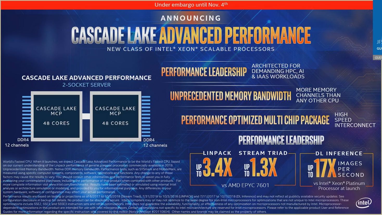
Each Cascade-AP lake processor will offer up to 48 cores, and in order to do this Intel is using a multi-chip package (MCP). At this point we believe that Intel is using two silicon dies in the package, specifically two ‘XCC’ dies which should be 28-core by design but will be only enabled up to 24-core per silicon die. Intel did confirm that these dies are connected by UPI over the package, and not with Intel’s EMIB technology. This is unfortunate, given how Intel has promoted its EMIB technology as an alternative to interposers, but we have yet to see it in a product that connects two high-powered chips together, as was originally envisioned when the technology was first announced. It does mean however that it can use the same silicon as will be found in the standard Xeon Scalable processors.
No information was given about TDP per processor, or pricing, PCIe lanes, memory capacity/support, frequencies, or variants. We were told that it will be launched at the same time as the full Cascade Lake family ‘in the first part of 2019’ (to directly quote). Intel did give some base performance numbers, suggesting that a processor scores 3.4x higher than an EPYC 7601 on Linpack and 1.3x higher on Stream Triad. Deep Learning inference, a major workload for these new parts, was quoted as scoring 17x the base Skylake-SP launch performance, which would be 1.55x the original quoted Cascade-SP launch performance with the new VNNI instructions.
Given the extra power requirements and extra memory requirements, we fully expect Intel to be using a new socket for this processor. Rather than LGA4367, with 4367-pins, there have been recent leaks suggesting that an LGA5903 socket be where Cascade-AP will end up, although Intel has not confirmed this. Intel did state that Cascade-AP will be shipping for revenue in Q3 2018 to its high-profile customers as part of its early access program, however widespread availability will be ‘in the first part of 2019’.
More Cores Per Socket, But Potentially a Worse 4S System
With this new type of processor, even given Intel’s previous competitive analysis of MCP designs, Intel is pushing up the number of cores per socket, and cores per 2S system. The 2S server market is one of Intel’s biggest across the whole company, and the idea is to offer more value. It’s hard to state the impact that Cascade-AP will have on the product portfolio, but it comes to mind that Intel is trying to condense a 4P system into a 2P system, though it probably won’t perform as well.
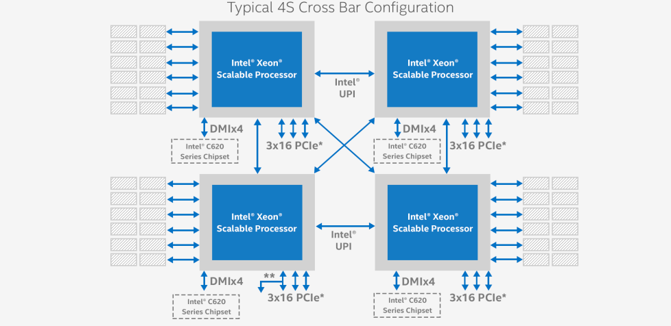
Take, for example, a 24-core 4P system, which has 96 cores total. Using Intel’s 3 UPI links, the communication between the four processors allows each processor to talk to each other processor in only one hop. Each processor has six channels of memory, access to 48 PCIe lanes, potential access to OmniPath, etc.
In a Cascade-AP two socket system, it all depends on how the links between the sockets are formed.
We already know that within a single package, the two silicon dies will talk to each other over UPI through the package. This is lower power than a socket-to-socket UPI link, and might take advantage of lower latency as well. That is all well and good.
But between the sockets is where questions will lie. If Intel is only using one UPI link between the sockets, then only one die from each socket will be connected. This is essentially a straight chain connectivity, meaning that to talk to a silicon die on the other socket, it may require two hops.
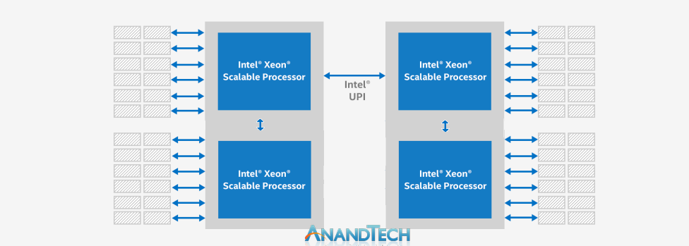
If Intel is using two UPI links between the sockets, then we have a situation similar to a Xeon Gold-2UPI system where the processors are arranged in a square and there is no cross-connection. This creates a communication imbalance between processors and memory which might be hard to predict unless the software can enumerate and deal with it effectively.
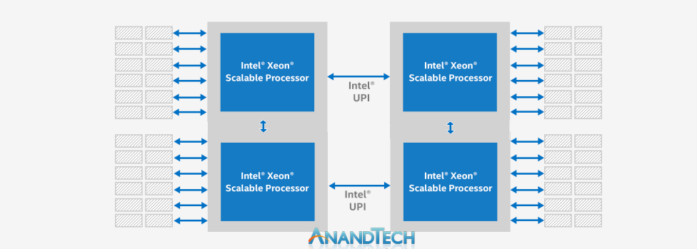
The other option is if Intel is using four UPI links between the sockets – two from each silicon die, to one each of the other silicon dies on the other processor. This is identical to a 4P 3UPI system, except that the dual socket configuration makes this all the more complex. It would require at least two UPI links to cross over each other with the traces on the motherboard. This either requires a thick motherboard (adds cost) or a control repeater chip that can do it easier. But even then, we’re dealing with a non-uniform memory architecture in each socket and between sockets with different latencies between the hops. At least in a natural 4S system, the arrangement can ensure latencies are equal.
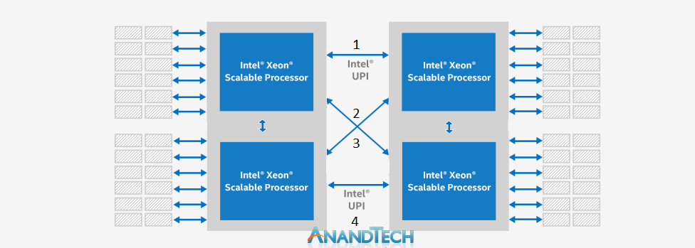
There’s also the question of PCIe lanes. Intel has not given a number, but we suspect it to be anywhere between 48 (24 per die) or 96 (48 per die) per socket. Which would be identical to a 4S system again.
Further to that, a question of frequencies. A current 24-core Xeon Platinum runs at 205W. Intel is not going to put the TDP at 410W when it puts two together – it will have to lower the frequency to hit something more suitable for the large socket. Add into that the complexity of supplying 48 cores with enough power to be competitive. With separate chips, each socket can have higher frequencies.
The only saving grace here would be actual physical volume. Some datacenters are all about compute density, and for some providers looking to deploy mass x86 CPUs in their offering, this could be a winner with them. Intel has repeatedly cited that Xeon-based inference as a major source of customers, hence the inclusion of features like VNNI on Cascade Lake to help drive that market.
Timeline for Cascade Lake and Cascade Lake-AP
Intel stated that they are shipping processors for revenue to select customers as part of its early adopter program. The new parts will be launched in the first part of 2019, with the full Cascade Lake family (SP and AP) being launched at the same time. We asked a series of pertinent questions after our briefing, however Intel was unwilling to answer anything additional to our presentation. Some further information (or demonstrations) might be seen at the Supercomputing 2018 conference happening next week.


91 Comments
View All Comments
mode_13h - Monday, November 5, 2018 - link
16 memory channels, only if you count the 4 Optanes. But I think it's only 12 channels of DDR4.eddman - Monday, November 5, 2018 - link
I'm wondering about memory channels too. Each die has two three channel memory controllers, 12 channels in total. Did they deliberately not activate all controllers or they simply couldn't technically do that?eddman - Monday, November 5, 2018 - link
Scratch that. I somehow missed the first memory part and misread the 4S system part.eddman - Monday, November 5, 2018 - link
Scratch that. I somehow missed the first memory part and misread the 4S system example.jjj - Monday, November 5, 2018 - link
Hey, they found the glue!SaturnusDK - Monday, November 5, 2018 - link
Is Intel sniffing glue? I know it's a last ditch attempt at staying relevant before the EPYC 2 reveal tomorrow but even then this is a poor attempt.yeeeeman - Monday, November 5, 2018 - link
If AMD Rome has 64 cores per CPU, then Intel is done on the server front. PeriodDigitalFreak - Monday, November 5, 2018 - link
I love these comments. Even if AMD's Rome blows the 48c Cascade Lake out of the water, Intel is far from "done" on any front.goatfajitas - Monday, November 5, 2018 - link
If AMD has 256 cores per CPU at half the price of Intel's 48 core with performance to match Intel still isnt done. That's just not how server sales work.- Now if AMD had and maintained that lead for 5+ years with performance and reliability on the whole platform Intel would have some serious trouble.
Icehawk - Monday, November 5, 2018 - link
Yup, my director won’t even consider a test Epyc box - “not proven”.