Naples, Rome, Milan, Zen 4: An Interview with AMD CTO, Mark Papermaster
by Ian Cutress on November 12, 2018 9:15 AM EST- Posted in
- CPUs
- AMD
- Interview
- Zen
- Vega
- 7nm
- AMD Instinct
- EPYC
- Infinity Fabric
- Rome
- Mark Papermaster
At AMD’s Next Horizon event this week, the company disclosed for the first time the layout of its next generation EPYC processor, the new Vega Radeon Instinct datacenter compute accelerators, as well as a strong confidence that its execution on 7nm will be a big win. If there’s anyone at AMD prepared to talk about execution, it’s the Chief Technology Officer and SVP of Technology and Engineering, Mark Papermaster.
Matching and Exceeding Expectations
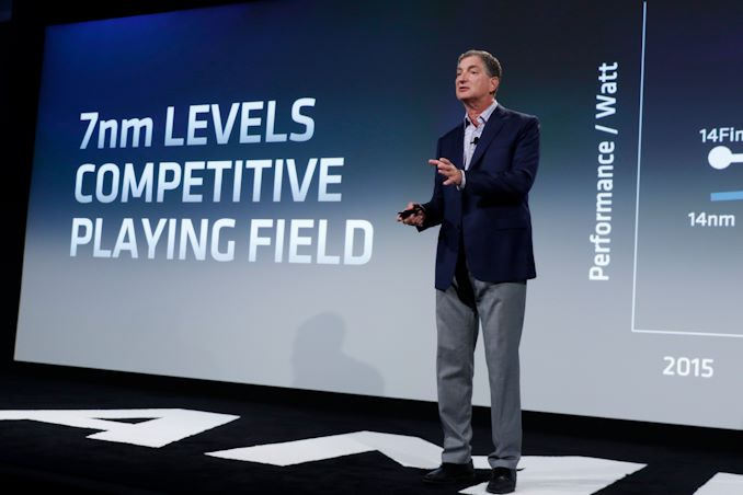
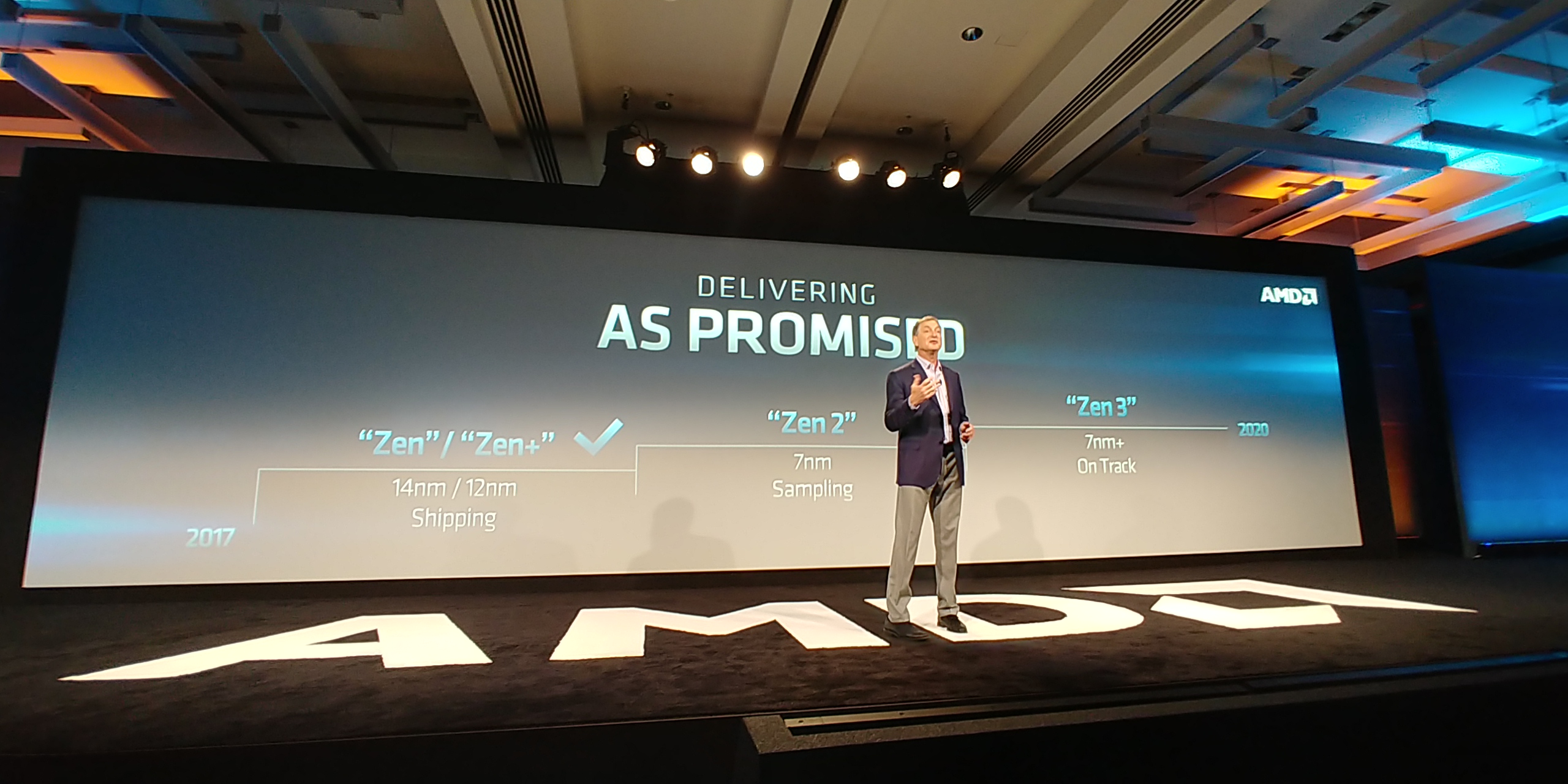
The goal of AMD’s event in the middle of the fourth quarter of the year was to put into perspective two elements of AMD’s strategy: firstly, its commitment to delivering a 7nm Vega based product by the end of the year, as the company promised in early 2018, but also to position its 7nm capabilities as some of the best by disclosing the layout of its next generation enterprise processor set to hit shelves in 2019. This is, of course, a far cry from AMD during the Bulldozer days – the excitement in the presentation room from AMD’s executive staff was palpable. It’s rare to see so much latent energy and excitement in what could have been a series of dull presentations, but the ability for AMD to execute and compete in this new Zen era is one that gets the adrenaline going up and down the employee chain.
 Ian Cutress AnandTech |
 Mark Papermaster AMD |
For us, the press, information is our currency. AMD showing off its new 7nm EPYC and 7nm Instinct designs was a nice touch to the events of the day, however we always want more. Not only is AMD putting down its capabilities today, but it is putting expectations through its roadmap for investors and customers in the months and years ahead. We sat down with AMD’s CTO, Mark Papermaster, to see if we could squeeze some of the finer details about both AMD’s strategy and the finer points of some of the products from the morning sessions.
AMD’s Vision of the Datacenter
Ian Cutress: Is AMD all about the roadmaps now?
Mark Papermaster: I’m happy about today is that it really reaffirms to the industry AMD’s execution. We set out an ambitious roadmap, and we are proving our mettle.
IC: When you say that you made decisions for this product 3-5 years ago, you weren’t joking, were you? Decisions you are making today are then for products set in 2021 and beyond?
MP: Absolutely correct. You really have to call the ball right in this industry. If you don’t, you create a gap – a significant multi-year gap.
IC: Forrest explained on the stage that the datacenter of today is very different to the datacenter ten years ago (or even 3-5 years ago). What decisions are you making today to predict the datacenter of the future?
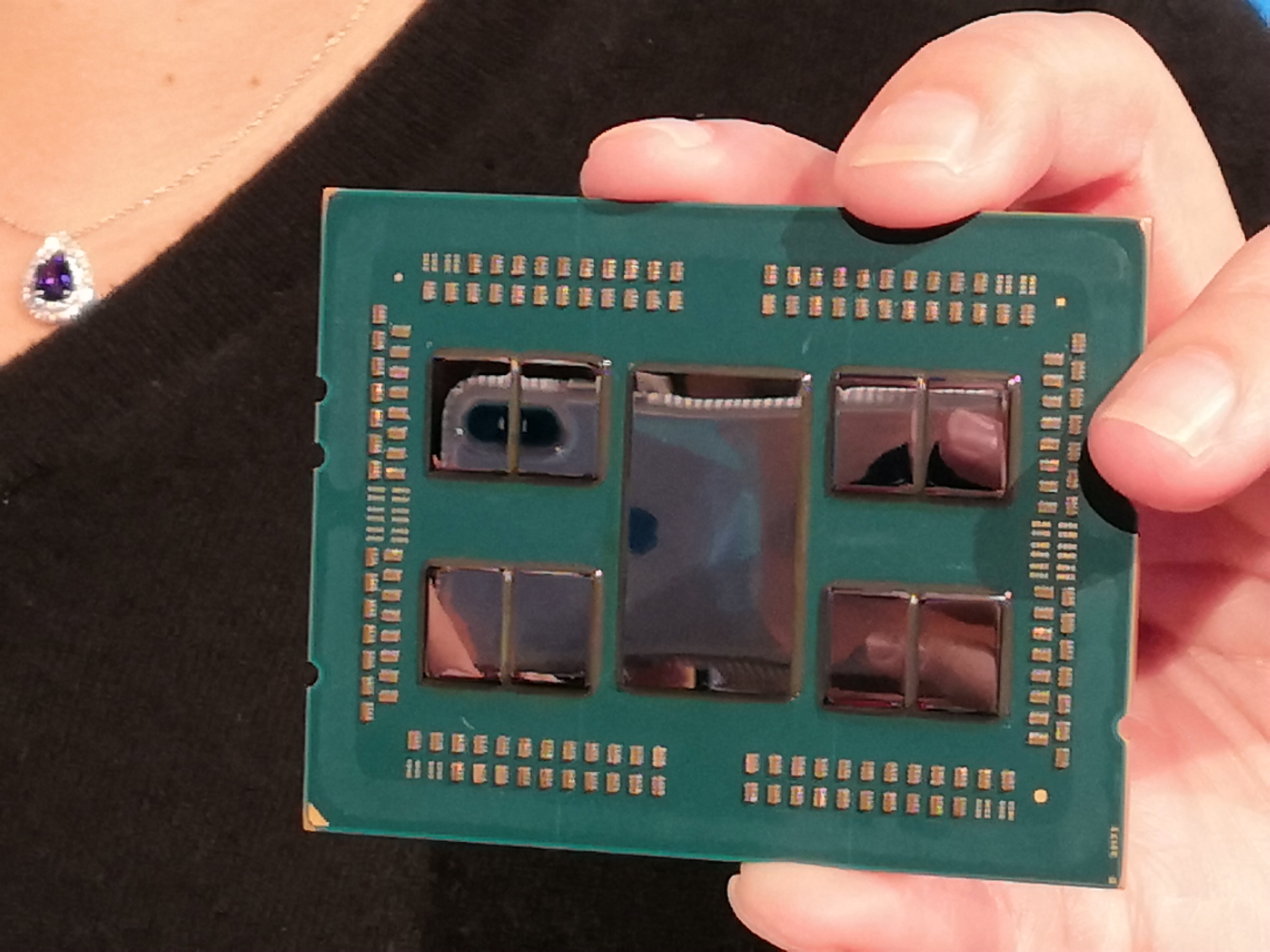
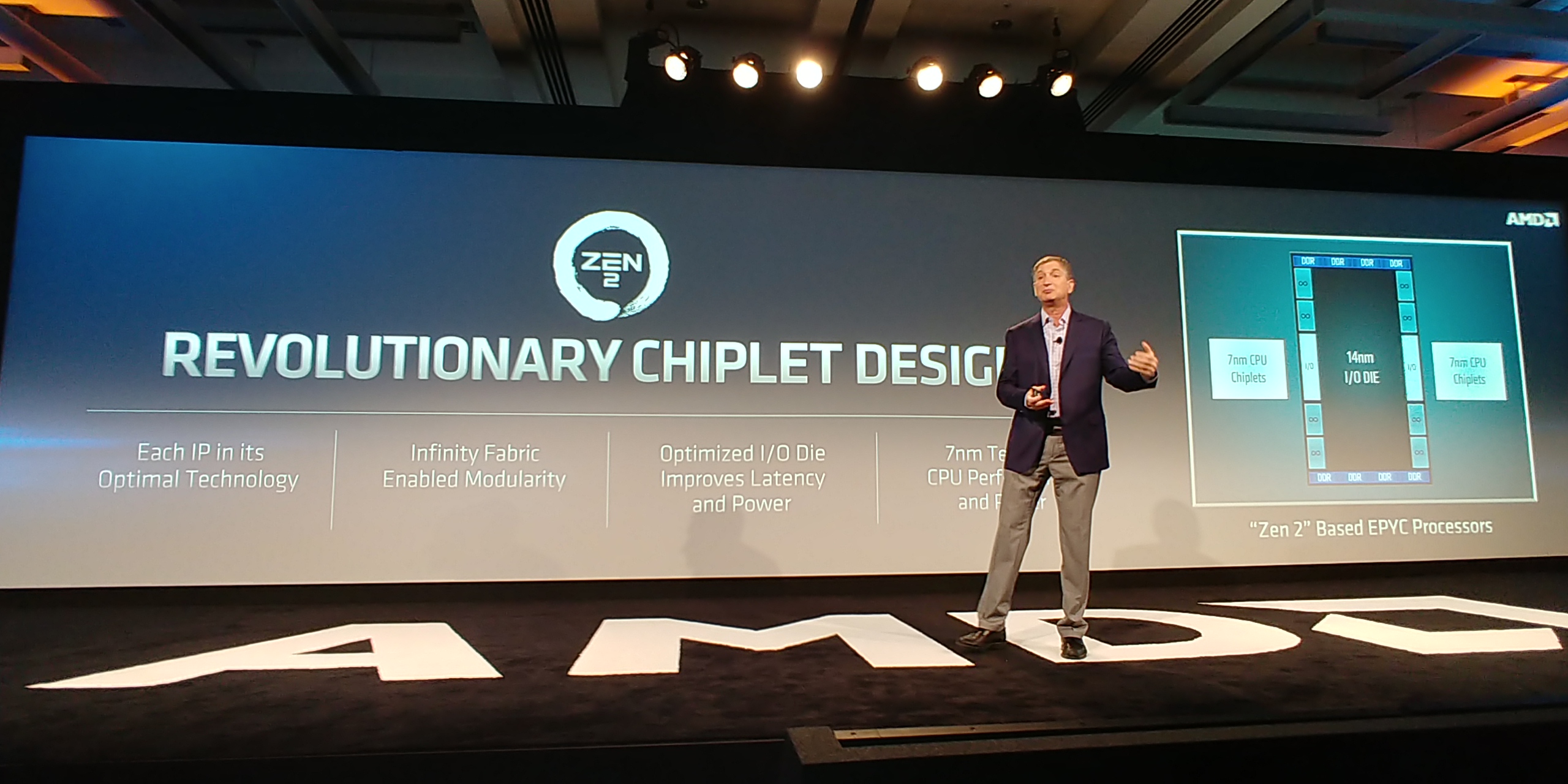
MP: We believe we will be positioned very well – it all ties back to my opening comments on Moore’s Law. We all accept that the traditional Moore’s Law is slowing down, and that while process does still matter you have to be agile about how you put the pieces together, otherwise you cannot win. We leveraged ourselves to have scalability in our first EPYC launch. We leveraged our ability in our chiplet approach here to combine really small 7nm CPU dies with tried and proven 14nm for the IO die. That modularity only grows in importance going forward. We’ve stated our case as to where we believe it is necessary to keep pace on a traditional Moore’s Law growth despite the slowing of the process gains per node and the length of time between major semiconductor nodes. I think you’ll see others adopt what we’ve done with the chiplet approach, and I can tell you we are committed.
We’ve re-architected what we do to allow ourselves to be agile and putting our IPs together and eventually this will be an ecosystem based on our IPs. That ecosystem will have others over time because who can predict exactly which ML accelerators may be disruptive in the market, and who can predict what new memory configuration might provide an advantage. Those companies that are agile and adaptable will win and this is the crux of AMD’s strategy. We will be able to drive the base of the CPU and GPU roadmap that keeps us at the front of the leadership and have a modularity and flexibility to adapt to the workloads as they merge.
Diving into Rome
IC: Can you confirm where the parts of Rome are manufactured?
MP: Chiplets on TSMC 7nm, the IO die is on GlobalFoundries 14nm.
IC: With all the memory controllers on the IO die we now have a unified memory design such that the latency from all cores to memory is more consistent?
MP: That’s a nice design – I commented on improved latency and bandwidth. Our chiplet architecture is a key enablement of those improvements.
IC: When you say improved latency, do you mean average latency or peak/best-case latency?
MP: We haven’t provided the specifications yet, but the architecture is aimed at providing a generational improvement in overall latency to memory. The architecture with the central IO chip provides a more uniform latency and it is more predictable.
IC: There are a lot of questions surrounding AMD’s cache hierarchy that you probably can’t answer, but can you at least state if the IO chip has a cache inside?
MP: All the details within the IO die and beyond what we said today will be forthcoming at our EPYC 2 launch.
IC: The IO die as showed in the presentation looked very symmetrical, almost modular in itself. Does that mean it can be cut into smaller versions?
MP: No details at this time.
IC: Do the chiplets communicate with each other directly, or is all communication through the IO die?
MP: What we have is an IF link from each CPU chiplet to the IO die.
IC: When one core wants to access the cache of another core, it could have two latencies: when both cores are on the same chiplet, and when the cores are on different chiplets. How is that managed with a potentially bifurcated latency?
MP: I think you’re trying to reconstruct the detailed diagrams that we’ll show you at the product announcement!
IC: Under the situation where we now have a uniform main memory architecture, for on-chip compared to chip-to-chip there is still a near and a far latency…
MP: I know exactly where you’re going and as always with AnandTech it’s the right question! I can honestly say that we’ll share this info with the full product announcement.
IC: One of the biggest changes when Zen came out was the op-cache, and AMD is saying it’s now larger.
MP: You know we made so many front-end changes on Zen and we had ideas of even more what we could do, but as you know at some point we have to bring the product to market. So some ideas end up in the next generation where we get the low hanging fruit and also implement new technologies. The engineers had many more ideas after Zen, some of which made it into Zen 2, and we will see these sorts of generational improvements. They are very nice enhancements in Zen 2, including improved efficiency at the front end to feed the revamped execution units.
IC: With the FP units now capable of doing 256-bit on their own, is there a frequency drop when 256-bit code is run, similar to when Intel runs AVX2?
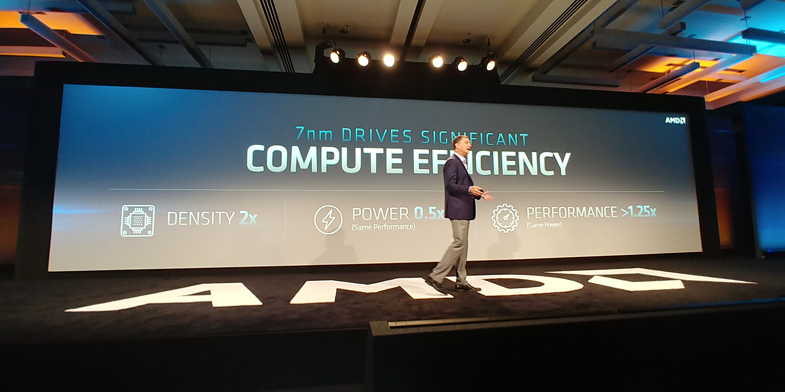
MP: No, we don’t anticipate any frequency decrease. We leveraged 7nm. One of the things that 7nm enables us is scale in terms of cores and FP execution. It is a true doubling because we didn’t only double the pipeline with, but we also doubled the load-store and the data pipe into it.
IC: Now the Zen 2 core has two 256-bit FP pipes, can users perform AVX512-esque calculations?
MP: At the full launch we’ll share with you exact configurations and what customers want to deploy around that.
IC: AMD’s consumer side actively promotes technologies such as Precision Boost 2 and XFR2 to manage frequency and load with other variables in the mix. Are any of those implemented in Rome?
MP: Details to follow at the product announcement!
IC: Can you go into detail about the additional hardware Spectre mitigations?
MP: I simply call it a hardening. We shared the approaches that we took with microcode and software for Spectre (Zen is not affected by Meltdown or Foreshadow), you can read our whitepapers on it, and this is about alleviating the microcode from having to intercept and take those actions. The idea is that if we harden that in hardware it becomes more ubiquitous. More info to come on that, but we did want to include a mention of the improvements in the hardware mitigations.
The Rome Product
IC: Will Rome aim for a level of price parity with Naples?
MP: We haven’t announced our focus on pricing. I think this is how to think about it: what you have seen from AMD is what we’ve targeted comes from a design point, and what we’ve shared with you today is what we are delivering. Today we said that for a given power envelope, for a given socket configuration, Rome will offer a doubling of core performance or a quadrupling in floating point performance. Pricing will come when the products are closer to shipping, and we have performance targets per socket. We will always be price competitive too, especially in performance per socket.
IC: Where does Rome sit with CCIX support?
MP: We didn’t announce specifically those attributes beyond PCIe 4.0 today, but I can say we are a member of CCIX as we are with Gen Z. Any further detail there you will have to wait until launch. Any specific details about the speeds, feeds, protocols, are coming in 2019.
IC: There have been suggestions that because AMD is saying that Rome is coming in 2019 then that means Q4 2019.
MP: We’re not trying to imply any specific quarter or time frame in 2019. If we look at today’s event, it was timed it to launch our MI60 GPU in 7nm which is imminent. We wanted to really share with the industry how we’ve embraced 7nm, and preview what’s coming out very soon with MI60, and really share our approach on CPU on Zen 2 and Rome. We’re not implying any particular time in 2019, but we’ll be forthcoming with that. Even though the GPU is PCIe 3.0 backwards compatible, it helps for a PCIe 4.0 GPU to have a PCIe 4.0 CPU to connect to!
IC: With Rome being up to 64 cores, are you seeing diminishing returns promoting dual socket configurations?
MP: No – there’s such an insatiable demand for compute and it’s about TCO. Of course, we are ensuring that real value is delivered. We’re working with ISVs to make sure they can support the increased core count as we’re blowing through what they envisioned what would be the number of cores they support on a per socket basis. All that work is well underway and at launch we will have the ISV community with us.
IC: Part of the launch of Naples was the communication that users could replace a two socket system with one Naples. Now you can replace a 2S Naples with one socket Rome!
MP: It’s very simple in this industry – our view at AMD is that we’re going to deliver the best TCO (total cost of ownership) value we can. That’s the best strategy for us, to be the upstart coming back in and fighting our way to maximize our market share gain. This is a battle and we’re bringing every tool in the shed.
IC: We expect lower core counts of Rome to eventually exist. This could mean fewer cores enabled per chiplet or just fewer chiplets entirely?
MP: We didn’t announce details, but you can see the physical modularity given the layout shared today. What you’re seeing today is eight 8-core clusters so that the easiest physical modularity is on a chiplet basis.
IC: AMD has already committed that Milan, the next generation after Rome, will have the same socket as Rome. Can you make the same commitment with Zen 4 that was shown on the roadmap slides?
MP: We’re certainly committed to that socket continuity through Milan, and we haven’t commented beyond that. Obviously at some point the industry transitions to PCIe 5.0 and DDR5 which will necessitate a socket change.
IC: So one might assume that an intercept might occur with Zen 4?
MP: No comment (!)

Revisiting Infinity Fabric
IC: One of the key aspects in AMD’s portfolio is the Infinity Fabric, and with Rome you have stated that AMD is now on its second generation IF. Do you see an end in its ability to scale down in process node but also scale out to more chiplets and different IP?
MP: I don’t see an end because the IF is made of both of Scalable Data Fabric and a Scalable Control Fabric. The SCF is the key to giving the modularity and that’s an architectural product. With our SDF we are very confident on the protocols we developed. The SCF protocols are based on the rich history we have with HyperTransport and we are committed in it generationally to improve bandwidth and latency every generation. IF is important when it applies to on chip connectivity, but it can go chip to chip like we did with EPYC, and also with Vega Radeon Instinct in connecting GPU to GPU. For the chip to chip IF, you are also dependent on the package technology. We see tremendous improvements in package technology over the next five years.
IC: One of the key aspects of IF is that it has started becoming a big part of the power consumption on EPYC. What is AMD doing to manage that power?
MP: Fabrics going forward have to be developed with the same energy efficiency optimizations in mind as with our core engines, such as our CPUs and GPUs. When we started with IF in our CPUs, we started with tremendous energy efficiency for our high performance objectives. We are making generationally excellent performance per watt improvements in our core engines, and we have IF on the same track. Energy efficiency is required in any of the markets that we serve. Therefore we are driving every IP that we develop in the company to improve energy efficiency each and every generation.
IC: Should we expect companies that aren’t AMD to implement IF?
MP: We haven’t announced any plan to license that IP, as we are not in the IP licensing business. But we certainly I could envision partnerships through our semicustom business working with our partners where the right business makes sense for both parties.
IC: With chiplets connected via IF on Rome, if a customer wanted a semi-custom design with different IP, such as a GPU or an AI block or an FPGA, would that be possible? (Say for example, a console?)
MP: Our semi-custom group is wide open to talk to customers to brainstorm! What excites me about the chiplet approach is that I think it’s going to disrupt the industry. It’s going to change the way the industry dreams of different configurations. Some might be right, and I can guarantee that someone will conjure up ten other ones that we didn’t think of! Honestly I think it is a disruptive force that is just nascent, just starting right now.
IC: With IF on 7nm, it offers 100 GB/s GPU to GPU connectivity. One of your competitors has something similar which allows both GPU-GPU and CPU-GPU connectivity. Currently with Rome, PCIe 4.0 has been announced from CPU to GPU but not IF. What has AMD’s analysis been on that CPU to GPU link?
MP: We haven’t announced applying the IF between the CPU and GPU and while it is certainly feasible, it is likely just dependent when workloads could truly leverage that protocol being applied, when the full coherency is required across both CPU and GPU. It is certainly feasible, but we haven’t announced it at this time.
AMD on Design and Manufacturing
IC: You mentioned on stage that AMD has leapfrogging design teams. How do you manage keeping positive aspects of the design if the teams are out of sync with each other?
MP: So to be clear, we have one architecture team but two implementation teams. Best practices of architecture are shared from generation to generation. The implementation teams all work under the same internal organizational team, and we’ve done everything to lower the barrier of best practices and innovation sharing within those teams. If you look in the industry, often at times we see that companies end up with competing microprocessor design teams. I’m not a believer that that is the best way to get the best microprocessor. I think in order to get ahead you need parallel efforts, you have to partition the implementation, but I’m a big believer that you come out way ahead when the teams brainstorm together on the best approaches and microarchitecture changes for performance improvement.
IC: On personnel, AMD has recently been shedding key talent to a major competitor, mostly in graphics. How is AMD approaching this alongside the inevitable competition in the GPU market which is set to follow in several years?
MP: We are constantly refreshing our talent – we have brought on tremendous talent year in and year out. AMD is recognized in the industry as an incredibly innovative company and one that is on the rise as they see our share growing in the industry and so we are attracting great talent and from time to time we have folks leave as with any company. We are still full speed ahead and we are very excited with some of the folks that have come and knocked on our door to join our team.
IC: AMD has had a strong relationship with TSMC for many years which is only getting stronger with the next generation products on 7nm, however now you are more sensitive to TSMC’s ability to drive the next manufacturing generation. Will the move to smaller chiplets help overcome potential issues with larger or dies, or does this now open cooperation with Samsung given that the chip sizes are more along the lines of what they are used to?
MP: First off, the march for high performance has brought us to Zen 2 and the ability to leverage multiple technology nodes. What we’re showing with Rome is a solution with two foundries with two different technology nodes. It gives you an idea of the flexibility in our supply chain that we’ve built in, and gives you explicit example of how we can work with different partners to achieve a unified product goal. On the topic of Samsung, we know Samsung very well and have done work with them.
IC: You expected that when you came out with 7nm in 2018/2019 that the process technology AMD used would be at parity with the competition, and your major competitor would already have 10nm products on the shelf. Today you have stated that you will be ahead of that expectation. How does AMD realign future performance goals in a situation where you are no longer playing catch-up?
MP: We can’t ever be anything other than pressing performance up. It’s a great time to be a customer of high performance! Why? Because we have competition back! When competition is there, all the players will be running as fast as they can and that is what I can guarantee from AMD. We’re going to be pressing to add performance every generation and deliver that value to our customers’ workloads.
IC: You said 7nm is meant to be a long lived node, and variations of 7nm are expected from TSMC with EUV. What resources are AMD putting in place for a post-7nm world?
MP: We have a team that is constantly working with that, like the CPU team that is looking ahead, and we do the same with our foundry preparedness teams. This includes design options, and we work with the various supporting industries as well as working with the foundries. We are always looking into future nodes across the industry.
Many thanks to Mark and his team for their time!


57 Comments
View All Comments
Freeb!rd - Friday, November 16, 2018 - link
The benefits of 3D Xpoint as a memory DIMM has a very limited use case, at least in its current state. That may change in future versions, but that remains to be seen.Carmen00 - Monday, November 12, 2018 - link
This was amazing, Ian. Very insightful, probing and relevant questions on many different fronts while not being pushy at all! You have a real knack for this. Loved this interview, loved the interactions - "as always with AnandTech it’s the right question!", I couldn't have said it better myself. Kudos to you and Mark.A quick question on the transcription. In one of Mark's answers, it's transcribed as "adapt to the workloads as they merge". Did he say "merge", or "emerge"? Both are plausible. Could you confirm that your transcription is correct?
eva02langley - Tuesday, November 13, 2018 - link
What I get from it is that Infinity Fabric is that, maybe, it is what will really push AMD forward in the future. I am hoping they have IP and patents in place. If Intel had to pay license fees for their EMIB design, it would be hilarious.Kevin G - Tuesday, November 13, 2018 - link
Mark dances around an obvious upgrade path: to bring Zen 3 to market, AMD might be able to leverage the existing IO hub chip. Ditto for Zen 4. He is correct that DDR5/PCIe 5.0 may require a new socket but the chiplets are now effectively independent of that restriction (only the on package bus matters here!). This strategy permits asynchronous development of the CPU side and the IO side now.oleyska - Thursday, November 15, 2018 - link
Hey you want zen3 on ddr4, use last gen i/O chip.zen3 on DDR5, ohh here is the next gen I/O chip.
the 7nm+ chips are the same and production line to rule all the cpu's.
peevee - Tuesday, November 13, 2018 - link
"So one might assume that an intercept might occur with Zen 4?"What does the question mean? "Intercept"?
GreenReaper - Wednesday, November 14, 2018 - link
It's a weird way of asking "So Zen 4 might be the point where you need a new socket?"You could view it in the context of the subsequent graph where the intercept is where one line meets the other. Although it's not clear that what they're talking about there (promoted feature size) has anything to do with when they move to a new socket with DDR5 and PCIe 5.0 support.
yagma - Tuesday, November 13, 2018 - link
Have you patched the RYZENFALL, FALLOUT, CHIMERA, MASTERKE in these new chipsets?Its been 8 months since Mark Papermaster, Senior Vice President and Chief Technology Officer at AMD has acknowledged hardware level RYZENFALL, FALLOUT, CHIMERA, MASTERKE vulnerabilities, claiming "AMD will provide additional updates on both our analysis of these issues and the related mitigation plans in the coming weeks," well its been 8 months and they opted for a total blackout; 8 months and the greatest chipset level vulnerabilities AMD's history are apparently spreading freely and openly around the globe. It appears AMD doesn't have any concern for their customers safety, be it corporate, business, or power-users.
Intel made their vulnerabilities front page news, and initiated highly publicized steps to mitigate against them. Is AMD working on recalling these chipsets to have them refurbed? What are you doing to educate people and fix this problem?
Is it possible to disable the PSP? Snowden asked AMD to opensource PSP for this very reason.
Fritzkier - Tuesday, November 13, 2018 - link
I've seen this post on reddit and some other sites too.Don't copy paste your comments on EVERY AMD related thread... At least make a new one or something instead of copy paste...
1. The vulnerability isn't significant (because it needs admin rights)
2. They already sent the patches to their partners (see tomhardware article on May 2nd.)
3. You're a shill, stop copy-paste an exact same post. (At least make your own paragraph, geez)
quadibloc - Thursday, November 22, 2018 - link
Indeed, AMD can't get complacent because Intel was having problems with 10nm. For one thing, Intel is now claiming it's overcome those problems. For another, Intel has already hired TSMC to make chips for them, so they can get 7nm chips from TSMC just as easily as AMD if worst came to worst.