Upgrading from an Intel Core i7-2600K: Testing Sandy Bridge in 2019
by Ian Cutress on May 10, 2019 10:30 AM EST- Posted in
- CPUs
- Intel
- Sandy Bridge
- Overclocking
- 7700K
- Coffee Lake
- i7-2600K
- 9700K
Sandy Bridge: Inside the Core Microarchitecture
In the modern era, we are talking about chips roughly the size of 100-200mm2 having up to eight high performance cores on the latest variants of Intel’s 14nm process or AMD’s use of GlobalFoundries / upcoming with TSMC. Back with Sandy Bridge, 32nm was a different beast. The manufacturing process was still planar without FinFETs, implementing Intel’s second generation High-K Metal Gate, and achieving 0.7x scaling compared to the larger 45nm previous. The Core i7-2600K was the largest quad core die, running at 216 mm2 and 1.16 billion transistors, which compared to the latest Coffee Lake processors on 14nm offer eight cores at ~170 mm2 and over 2 billion transistors.
The big leap of the era was in the microarchitecture. Sandy Bridge promised (and delivered) a significant uplift in raw clock-for-clock performance over the previous generation Westmere processors, and forms the base schema for Intel’s latest chips almost a decade later. A number of key innovations were first made available at retail through Sandy Bridge, which have been built upon and iterated over many times to get to the high performance we have today.
Through this page, I have largely used Anand’s initial report into the microarchitecture back in 2010 as a base, with additions based on the modern look on this processor design.
A Quick Recap: A Basic Out-of-Order CPU Core
For those new to CPU design, here’s a quick run through of how an out-of-order CPU works. Broadly speaking, a core is divided into the front end and back end, and data first comes into the front end.

In the front end, we have the prefetchers and branch predictors that will predict and pull in instructions from the main memory. The idea here is that if you can predict what data and instructions are needed next before they are needed, then you can save time by having that data close to the core when needed. The instructions are then placed into a decoder, which transforms the byte code instruction into a number of ‘micro-operations’ that the core can then use. There are different types of decoders for simple and complex instructions – simple x86 instructions map easily to one micro-op, whereas more complex instructions can decode to more – the ideal situation is a decode ratio as low as possible, although sometimes instructions can be split into more micro-ops if they can be run in parallel together (instruction level parallelism, or ILP).
If the core has a ‘micro-operation cache’, or uOp cache, then the results from each decoded instruction ends up there. The core can detect before an instruction is decoded if that particular instruction has been decoded recently, and use the result from the previous decode rather than doing a full decode which wastes power.
Now the uOps are now in an allocation queue, which for modern cores usually means that the core can detect if the instructions are part of a simple loop, or if it can fuse uOps together to make the whole thing go quicker, it can. The uOps are then fed into the re-order buffer, which forms the ‘back end’ of the core.
In the back end, starting with the re-order buffer, uOps can be rearranged depending on where the data each micro-op needs is. This buffer can rename and allocate uOps depending on where they need to go (integer vs FP), and depending on the core, it can also act as a retire station for complete instructions. After the re-order buffer, uOps are fed into the scheduler in a desired order to ensure data is ready and the uOp throughput is as high as possible.
In the scheduler, it passes the uOps into the execution ports (what does the compute) as required. Some cores have a unified scheduler between all the ports, however some split the scheduler depending on integer operations or vector style operations. Most out-of-order cores can have anywhere from 4 to 10 ports (or more), and these execution ports will do the math required on the data given the instruction passed through the core. Execution ports can take the form of a load unit (load from cache), a store unit (store into cache), an integer math unit, a floating point math unit, vector math units, special division units, and a few others for special operations. After the execution port is complete, the data can then be held for reuse in a cache, be pushed to main memory, while the instruction feeds into the retire queue, and finally retired.
This brief overview doesn’t touch on some of the mechanisms that modern cores use to help caching and data look up, such as transaction buffers, stream buffers, tagging, etc., some of which get iterative improvements every generation, but usually when we talk about ‘instructions per clock’ as a measure of performance, we aim to get as many instructions through the core (through the front end and back end) as many as possible – this relies on the decode strength of the front end, the prefetchers, the reorder buffers, and maximising the execution port use, along with retiring as many completed instructions as possible every clock cycle.
With this in mind, hopefully it will give context to some of Anand’s analysis back when Sandy Bridge was launched.
Sandy Bridge: The Front End
Sandy Bridge’s CPU architecture is evolutionary from a high level viewpoint but far more revolutionary in terms of the number of transistors that have been changed since Nehalem/Westmere. The biggest change for Sandy Bridge (and all microarchitectures since) is the micro-op cache (uOp cache).
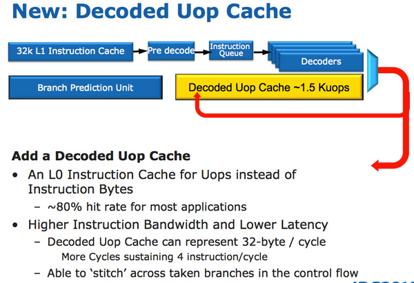
In Sandy Bridge, there’s now a micro-op cache that caches instructions as they’re decoded. There’s no sophisticated algorithm here, the cache simply grabs instructions as they’re decoded. When SB’s fetch hardware grabs a new instruction it first checks to see if the instruction is in the micro-op cache, if it is then the cache services the rest of the pipeline and the front end is powered down. The decode hardware is a very complex part of the x86 pipeline, turning it off saves a significant amount of power.
The cache is direct mapped and can store approximately 1.5K micro-ops, which is effectively the equivalent of a 6KB instruction cache. The micro-op cache is fully included in the L1 instructioncache and enjoys approximately an 80% hit rate for most applications. You get slightly higher and more consistent bandwidth from the micro-op cache vs. the instruction cache. The actual L1 instruction and data caches haven’t changed, they’re still 32KB each (for total of 64KB L1).
All instructions that are fed out of the decoder can be cached by this engine and as I mentioned before, it’s a blind cache - all instructions are cached. Least recently used data is evicted as it runs out of space. This may sound a lot like Pentium 4’s trace cache but with one major difference: it doesn’t cache traces. It really looks like an instruction cache that stores micro-ops instead of macro-ops (x86 instructions).
Along with the new micro-op cache, Intel also introduced a completely redesigned branch prediction unit. The new BPU is roughly the same footprint as its predecessor, but is much more accurate. The increase in accuracy is the result of three major innovations.
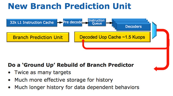
The standard branch predictor is a 2-bit predictor. Each branch is marked in a table as taken/not taken with an associated confidence (strong/weak). Intel found that nearly all of the branches predicted by this bimodal predictor have a strong confidence. In Sandy Bridge, the bimodal branch predictor uses a single confidence bit for multiple branches rather than using one confidence bit per branch. As a result, you have the same number of bits in your branch history table representing many more branches, which can lead to more accurate predictions in the future.
Branch targets also got an efficiency makeover. In previous architectures there was a single size for branch targets, however it turns out that most targets are relatively close. Rather than storing all branch targets in large structures capable of addressing far away targets, SNB now includes support for multiple branch target sizes. With smaller target sizes there’s less wasted space and now the CPU can keep track of more targets, improving prediction speed.
Finally we have the conventional method of increasing the accuracy of a branch predictor: using more history bits. Unfortunately this only works well for certain types of branches that require looking at long patterns of instructions, and not well for shorter more common branches (e.g. loops, if/else). Sandy Bridge’s BPU partitions branches into those that need a short vs. long history for accurate prediction.
A Physical Register File
Compared to Westmere, Sandy Bridge moves to a physical register file. In Core 2 and Nehalem, every micro-op had a copy of every operand that it needed. This meant the out-of-order execution hardware (scheduler/reorder buffer/associated queues) had to be much larger as it needed to accommodate the micro-ops as well as their associated data. Back in the Core Duo days that was 80-bits of data. When Intel implemented SSE, the burden grew to 128-bits. With AVX however we now have potentially 256-bit operands associated with each instruction, and the amount that the scheduling/reordering hardware would have to grow to support the AVX execution hardware Intel wanted to enable was too much.
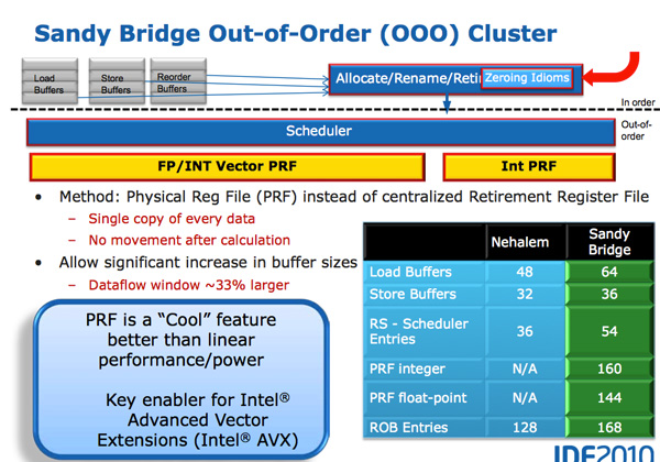
A physical register file stores micro-op operands in the register file; as the micro-op travels down the OoO engine it only carries pointers to its operands and not the data itself. This significantly reduces the power of the out of order execution hardware (moving large amounts of data around a chip eats tons of power), and it also reduces die area further down the pipe. The die savings are translated into a larger out of order window.
The die area savings are key as they enable one of Sandy Bridge’s major innovations: AVX performance.
AVX
The AVX instructions support 256-bit operands, which as you can guess can eat up quite a bit of die area. The move to a physical register file enabled Intel to increase the OoO buffers to properly feed a higher throughput floating point engine. Intel clearly believes in AVX as it extended all of its SIMD units to 256-bit wide. The extension is done at minimal die expense. Nehalem has three execution ports and three stacks of execution units:
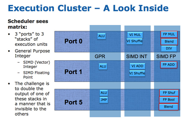
Sandy Bridge allows 256-bit AVX instructions to borrow 128-bits of the integer SIMD datapath. This minimizes the impact of AVX on the execution die area while enabling twice the FP throughput, you get two 256-bit AVX operations per clock (+ one 256-bit AVX load).
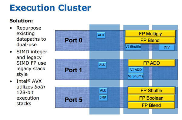
Granted you can’t mix 256-bit AVX and 128-bit integer SSE ops, however remember SNB now has larger buffers to help extract more instruction level parallelism (ILP).
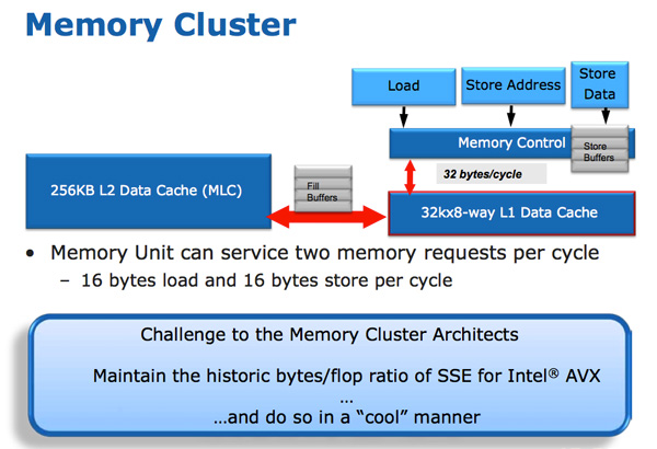
Load and Store
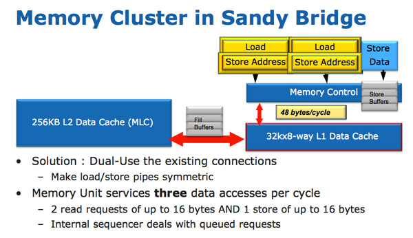
The improvements to Sandy Bridge’s FP performance increase the demands on the load/store units. In Nehalem/Westmere you had three LS ports: load, store address and store data.
In SNB, the load and store address ports are now symmetric so each port can service a load or store address. This doubles the load bandwidth compared to Westmere, which is important as Intel doubled the peak floating point performance in Sandy Bridge.
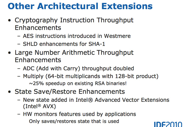
There are some integer execution improvements in Sandy Bridge, although they are more limited. Add with carry (ADC) instruction throughput is doubled, while large scale multiplies (64 * 64) see a ~25% speedup.


213 Comments
View All Comments
MxClood - Saturday, May 18, 2019 - link
In most test here it's around 100% or more increase in perf, i don't see where it's 40%.Also when you increase the graphics/resolution in gaming, the FPS are the same because the GPU becomes the bottleneck of FPS. You could put any futuristic cpu, the fps would be the same.
So why is it an argument about disappointing/abysmal performance.
Beaver M. - Wednesday, May 22, 2019 - link
After so many decades being wrong you guys still claim CPU power doesnt matter much in games.Youre wrong. Again. Common bottleneck today in games is the CPU, especially because the GPU advancement has been very slow.
Spunjji - Wednesday, May 22, 2019 - link
GPU advancement slowing down *makes the CPU less relevant, not more*. The CPU is only relevant to performance when it can't meet the bare minimum requirements to serve the GPU fast enough. If the GPU is your limit, no amount of CPU power increase will help.LoneWolf15 - Friday, May 17, 2019 - link
Is it abysmal because of the CPU though, or because of the software?Lots of software isn't written to take advantage of more than four cores tops, aside from the heavy hitters, and to an extent, we've hit a celing with clock speeds for awhile, with 5GHz being (not exactly, but a fair representation of) the ceiling.
AMD has caught up in a big way, and for server apps and rendering, it's an awesome value and a great CPU. Even with that, it still doesn't match up with a 9700K in games, all other things being equal, unless a game is dependent on GPU alone.
I think most mainstream software isn't optimized beyond a certain point for any of our current great CPUs, largely because until recently, CPU development and growth has stagnated. I'm really hoping real competition drives improved software.
Note also that it hasn't been like the 90s in some time, where we were doubling CPU performance every 16 months. Some of that is because there's too many limitations to achieving that doubling, both software and hardware.
I'm finding considerable speed boosts over my i7-4790K that was running at 4.4GHz (going to an i9-9900K running constantly at 4.7GHz on all cores) in regular apps and gaming (at 1900x1200 with two GTX 1070 cards in SLI), and I got a deal on the CPU, so I'm perfectly happy with my first mainboard/CPU upgrade in five years (my first board was a 386DX back in `93).
peevee - Tuesday, May 14, 2019 - link
Same here. i7-2600k from may 2011, with the same OCZ Vertex 3.8 years, twice the cores, not even twice the performance in real world. Just essentially overclocked to the max from the factory.
Remember when real life performance more than doubled every 2 years? On the same 1 core, in all apps, not just heavily multithreaded? Good thing AMD at least forced Intel go from 4 to 6 to 8 in 2 years. Now they need to double their memory controllers, it's the same 128 bits since what, Pentium Pro?
Mr Perfect - Friday, May 10, 2019 - link
Same here. Over the years I've stuffed it full of RAM and SSD and been pleased with the performance. I'm thinking it's time for it to go though.In 2016 I put a 1060 in the machine and was mildly disappointed in the random framerate drops in games (at 1200p). Assuming it was the GPU's fault, I upgraded further in 2018 to a 1070 Ti some bitcoin miner was selling for cheap when the market crashed. The average framerates went up, but all of the lows are just as low as they ever where. So either Fallout 4 runs like absolute garbage in certain areas, or the CPU was choking up both GPUs.
When something that isn't PCIe 3 comes out I suppose I can try again and see.
ImOnMy116 - Friday, May 10, 2019 - link
For whatever it's worth, in my experience Fallout 4 (and Skyrim/Skyrim SE/maybe all Bethesda titles) are poorly optimized. It seems their engine is highly dependent on IPC, but even in spite of running an overclocked 6700K/1080 Ti, I get frame drops in certain parts of the map. I think it's likely at least partially dependent on where your character is facing at any given point in time. There can be long draw distances or lots of NPCs near by taxing the CPU (i.e. Diamond City).Mr Perfect - Friday, May 10, 2019 - link
Yeah, that makes sense. F4's drops are definitely depended on location and where the character is facing for me too.The country side, building interiors and winding city streets you can't see very far down are just fine. Even Diamond City is okay. It's when I stand at an intersection of one of the roads that runs arrow straight through Boston or get up on rooftops with a view over the city that rates die. If the engine wants pure CPU grunt for that, then the 2600 just isn't up to it.
Strangely, Skyrim SE has been fine. The world is pretty sparse compared to F4 though.
Vayra - Monday, May 13, 2019 - link
Fallout 4 is simply a game of asset overload. That happens especially in the urban areas. It shows us that the engine is past expiry date and unable to keep up to the game's demands of this time. The game needs all those assets to at least look somewhat bearable. And its not efficient about it at all; a big part of all those little items also need to be fully interactive objects.So its not 'strange' at all, really. More objects = more cpu load and none of them can be 'cooked' beforehand. They are literally placed in the world as you move around in it.
Vayra - Monday, May 13, 2019 - link
This is also part of the reason why the engine has trouble with anything over 60 fps, and why you can sometimes see objects falling from the sky as you zone in.