TSMC’s 5nm EUV Making Progress: PDK, DRM, EDA Tools, 3rd Party IP Ready
by Anton Shilov on April 5, 2019 12:00 PM EST- Posted in
- Semiconductors
- EUV
- TSMC
- 5nm
- CLN5
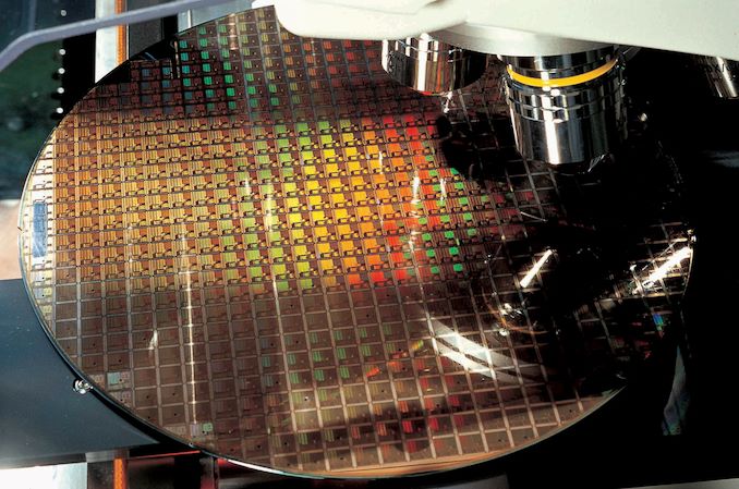
TSMC this week said that it has completed development of tools required for design of SoCs that are made using its 5 nm (CLN5FF, N5) fabrication technology. The company indicated that some of its alpha customers (which use pre-production tools and custom designs) had already started risk production of their chips using its N5 manufacturing process, which essentially means that the technology is on-track for high-volume manufacturing (HVM) in 2020.
TSMC’s N5 is the company’s 2nd generation fabrication technology that uses both deep ultraviolet (DUV) as well as extreme ultraviolet (EUV) lithography. The process can use EUVL on up to 14 layers (a tangible progress from N7+, which uses EUVL on four non-critical layers) to enable significant improvements in terms of density. TSMC says that when compared to N7 (1st Gen 7 nm, DUV-only), N5 technology will allow chip developers to shrink die area of their designs by ~45%, making transistor density ~1.8x higher. It will also increase frequency by 15% (at the same complexity and power) or reduce power consumption by 20% power reduction (at the same frequency and complexity).
| Advertised PPA Improvements of New Process Technologies Data announced by companies during conference calls, press briefings and in press releases |
||||||||
| TSMC | ||||||||
| 16FF+ vs 20SOC |
10FF vs 16FF+ |
7FF vs 16FF+ |
7FF vs 10FF |
7FF+ vs 7FF |
5FF vs 7FF |
|||
| Power | 60% | 40% | 60% | <40% | 10% | 20% | ||
| Performance | 40% | 20% | 30% | ? | same (?) | 15% | ||
| Area Reduction | none | >50% | 70% | >37% | ~17% | 45% | ||
TSMC finished development of N5 some time ago and its alpha customers with access to pre-production tools are already risk producing chips using the technology. Meanwhile, TSMC has finalized its 5 nm design rule manual (DRM), process design kits (PDKs), and SPICE (simulation program with integrated circuit emphasis) model for those clients who prefer to work with a stable version of design infrastructure.
Besides TSMC’s tools, chip developers can also use a comprehensive set of EDA (electronic design automation) tools from ANSYS, Cadence, Mentor Graphics, and Synopsys. TSMC says that EDA programs from the said companies fully support N5 DRM to ensure necessary accuracy, routability for optimized power, and other aspects of the technology. Obviously, all the tools have been certified by the contract maker of semiconductors.
Finally, TSMC and its partners have also developeda comprehensive N5 IP portfolio that is currently focused primarily on HPC and mobile SoCs. TSMC’s Foundation IP includes high-density and high-performance sets of standard cell libraries and memory compilers. Meanwhile, the company’s partners offer a variety of IP cores for N5 SoCs, including DDR, LPDDR, MIPI, PCIe, and USB PHYs.
“TSMC’s 5-nanometer technology offers our customers the industry’s most advanced logic process to address the exponentially growing demand for computing power driven by AI and 5G,” said Cliff Hou, Vice President of Research & Development/Technology Development at TSMC. “5-nanometer technology requires deeper design-technology co-optimization. Therefore, we collaborate seamlessly with our ecosystem partners to ensure we deliver silicon-validated IP blocks and EDA tools ready for customer use. As always, we are committed to helping customers achieve first-time silicon success and faster time-to-market.”
All the tools required for development of chips to be made using N5 fabrication technology are available from TSMC and its partners right now.
Related Reading
- TSMC: First 7nm EUV Chips Taped Out, 5nm Risk Production in Q2 2019
- TSMC Details 5 nm Process Tech: Aggressive Scaling, But Thin Power and Performance Gains
- TSMC Starts to Build Fab 18: 5 nm, Volume Production in Early 2020
Source: TSMC


31 Comments
View All Comments
Opencg - Friday, April 5, 2019 - link
to be honest 15% performance increase IS impressive at this point. in case your werent following we are approching a wall where structures wont have enough atoms to provide statistical reliability outside of flawless fabrication. we may be lucky to see 30% more performance increase from all future shrinks combined. significant performance increases are going to come from other means from now on. if you were thinking that 15% seems low then you just arent informedZolaIII - Saturday, April 6, 2019 - link
To get further performance and area improvements both new materials and structure of the gates are needed. Samsung for instance is working on cheap growing of Graphen (cheap enough to be used for battery cells but not neither perfect or big enough to make sizable wafer from it) and GAA structures while EAV which still has some error problems will reach its full potential in the future. I expect all three in next cuple of years & where we will go afterwards I really don't know.Santoval - Saturday, April 6, 2019 - link
"At 5nm we need of new transistors to have real advantages."TSMC will apparently not switch to GAA (Gate All Around) even at 5nm. I wonder if they saving that for the 3/4nm node.
Santoval - Saturday, April 6, 2019 - link
p.s. SemiWiki has predicted Intel will probably switch to GAA-FETs at 7nm. They also predict TSMC will switch to GAA at <5nm. Samsung might delay the switch for the ~2nm node.name99 - Monday, April 8, 2019 - link
Yeah, keep telling yourself that right up till Apple ships the ARM Macs, faster than Intel, on TSMC 5nm...Opencg - Monday, April 8, 2019 - link
i mean 15% performance increase for well over 15% price increase is hardly a leap forward. so objectively consumers will see little to no value increase from process alone. arm could bring architecture performance increases but honestly this is doubtful. esp when taking into account apples obsession with writing new code for everything to force obsolesence. if they would take thier time to develop a longterm codebase then instead of redoing everything with stupid gimmicks every time then MAYBE i could take this bold claim of your seriously. but no. its apple. and the performance value will go backwards due to process. so like 99.9999% your wrong and a fanboyZoolook - Friday, April 5, 2019 - link
Bigger "shrink" (area) than I'd suspected compared to the 7nm, good stuff, wonder who will be first Huawei or Apple?Opencg - Friday, April 5, 2019 - link
45% area shrink is about 25% closer elements.Diogene7 - Friday, April 5, 2019 - link
On a personal point of view, I find that TSMC 5nm node is quite a key technological milestone as it finally represent a more important usage of the off delayed EUV lithography in High Volume Manufacturing (HVM).It will still take several years and decades for the technology to mature, and then be routinely used by most foundries but it is very promising in terms of technologies that should appear between 2020 and 2040. I wish I would be born in 202O 😛...
Notmyusualid - Sunday, April 7, 2019 - link
+1. Should be called EXCITING UV....:)