AMD Zen 2 Microarchitecture Analysis: Ryzen 3000 and EPYC Rome
by Dr. Ian Cutress on June 10, 2019 7:22 PM EST- Posted in
- CPUs
- AMD
- Ryzen
- EPYC
- Infinity Fabric
- PCIe 4.0
- Zen 2
- Rome
- Ryzen 3000
- Ryzen 3rd Gen
CCX Size
Moving down in node size brings up a number of challenges in the core and beyond. Even disregarding power and frequency, the ability to put structures into silicon and then integrate that silicon into the package, as well as providing power to the right parts of the silicon through the right connections becomes an exercise in itself. AMD gave us some insight into how 7nm changed some of its designs, as well as the packaging challenges therein.
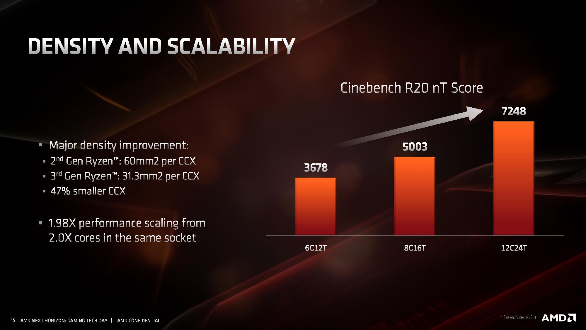
A key metric given up by AMD relates to the core complex: four cores, the associated core structures, and then L2 and L3 caches. With 12nm and the Zen+ core, AMD stated that a single core complex was ~60 square millimeters, which separates into 44mm2 for the cores and 16mm2 for the 8MB of L3 per CCX. Add two of these 60mm2 complexes with a memory controller, PCIe lanes, four IF links, and other IO, and a Zen+ zeppelin die was 213 mm2 in total.
For Zen 2, a single chiplet is 74mm2, of which 31.3 mm2 is a core complex with 16 MB of L3. AMD did not breakdown this 31.3 number into cores and L3, but one might imagine that the L3 might be approaching 50% of that number. The reason the chiplet is so much smaller is that it doesn’t need memory controllers, it only has one IF link, and has no IO, because all of the platform requirements are on the IO die. This allows AMD to make the chiplets extremely compact. However if AMD intends to keep increasing the L3 cache, we might end up with most of the chip as L3.
Overall however, AMD has stated that the CCX (cores plus L3) has decreased in size by 47%. That is showing great scaling, especially if the +15% raw instruction throughput and increased frequency comes into play. Performance per mm2 is going to be a very exciting metric.
Packaging
With Matisse staying in the AM4 socket, and Rome in the EPYC socket, AMD stated that they had to make some bets on its packaging technology in order to maintain compatibility. Invariably some of these bets end up being tradeoffs for continual support, however AMD believes that the extra effort has been worth the continued compatibility.
One of the key points AMD spoke about with relation to packaging is how each of the silicon dies are attached to the package. In order to enable a pin-grid array desktop processor, the silicon has to be affixed to the processor in a BGA fashion. AMD stated that due to the 7nm process, the bump pitch (the distance between the solder balls on the silicon die and package) reduced from 150 microns on 12nm to 130 microns on 7nm. This doesn’t sound like much, however AMD stated that there are only two vendors in the world with technology sufficient to do this. The only alternative would be to have a bigger bit of silicon to support a larger bump pitch, ultimately leading to a lot of empty silicon (or a different design paradigm).

One of the ways in order to enable the tighter bump pitch is to adjust how the bumps are processed on the underside of the die. Normally a solder bump on a package is a blob/ball of lead-free solder, relying on the physics of surface tension and reflow to ensure it is consistent and regular. In order to enable the tighter bump pitches however, AMD had to move to a copper pillar solder bump topology.
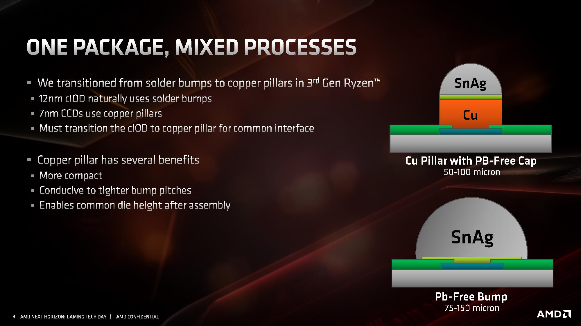
In order to enable this feature, copper is epitaxially deposited within a mask in order to create a ‘stand’ on which the reflow solder sits. Due to the diameter of the pillar, less solder mask is needed and it creates a smaller solder radius. AMD also came across another issue, due to its dual die design inside Matisse: if the IO die uses standard solder bump masks, and the chiplets use copper pillars, there needs to be a level of height consistency for integrated heat spreaders. For the smaller copper pillars, this means managing the level of copper pillar growth.
AMD explained that it was actually easier to manage this connection implementation than it would be to build different height heatspreaders, as the stamping process used for heatspreaders would not enable such a low tolerance. AMD expects all of its 7nm designs in the future to use the copper pillar implementation.
Routing
Beyond just putting the silicon onto the organic substrate, that substrate has to manage connections between the die and externally to the die. AMD had to increase the number of substrate layers in the package to 12 for Matisse in order to handle the extra routing (no word on how many layers are required in Rome, perhaps 14). This also becomes somewhat complicated for single core chiplet and dual core chiplet processors, especially when testing the silicon before placing it onto the package.
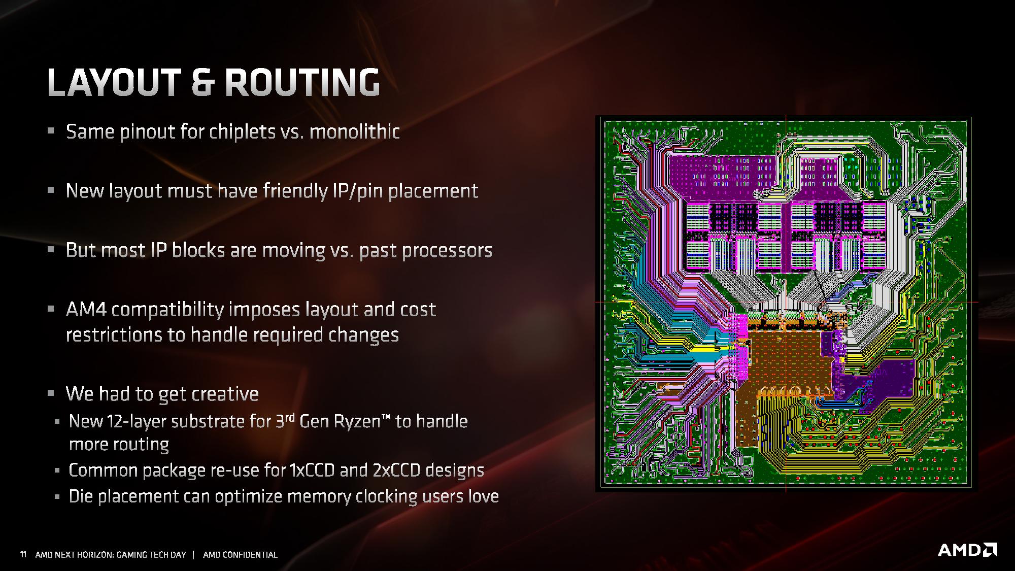
From the diagram we can clearly see the IF links from the two chiplets going to the IO die, with the IO die also handling the memory controllers and what looks like power plane duties as well. There are no in-package links between the chiplets, in case anyone was still wondering: the chiplets have no way of direct communication – all communication between chiplets is handled through the IO die.
AMD stated that with this layout they also had to be mindful of how the processor was placed in the system, as well as cooling and memory layout. Also, when it comes to faster memory support, or the tighter tolerances of PCIe 4.0, all of this also needs to be taken into consideration as provide the optimal path for signaling without interference from other traces and other routing.


216 Comments
View All Comments
Targon - Thursday, June 13, 2019 - link
The TDP figures are always a bit vague, because it is about the heat generation, not about power draw. A higher TDP on a chip with the same number of cores on the same design could indicate that it will overclock higher. Intel always sets the TDP to the base clock speed, while AMD has been more about what can be expected in normal usage. The higher the clock speed, the more power will be required, and the higher the amount of heat will be that needs to be handled by the cooler.So, if a chip has a TDP of 105W, then in theory, you should be able to get away with a cooler that can handle 105W of heat output, but if that TDP is based only on the base clock speed, you will want a better cooler to allow for turbo/boost for sustained periods.
wilsonkf - Monday, June 10, 2019 - link
We want faster memory for Zen/Zen+ because we want higher IF clock, so cutting the IF clock by half to enable higher memory freq. does not make sense. However the improved IF could move the bottleneck somewhere else.AlexDaum - Tuesday, June 11, 2019 - link
It seems like IF2 can not hit frequencies higher than about 3733MHz DDR (so 1,8GHz real frequency) for some reason, so they added the ability to scale it down to have higher memory clocks. But it is probably only worth it if you can overclock memory a lot higher than 3733, so that the IF clock gets a bit higher againXyler94 - Tuesday, June 11, 2019 - link
If I recall, IF2's clock speed is decoupled from RAM speed.Cooe - Tuesday, June 11, 2019 - link
This is wrong Xyler. Still completely connected.Xyler94 - Thursday, June 13, 2019 - link
Per this exact Article:"One of the features of IF2 is that the clock has been decoupled from the main DRAM clock. In Zen and Zen+, the IF frequency was coupled to the DRAM frequency, which led to some interesting scenarios where the memory could go a lot faster but the limitations in the IF meant that they were both limited by the lock-step nature of the clock. For Zen 2, AMD has introduced ratios to the IF2, enabling a 1:1 normal ratio or a 2:1 ratio that reduces the IF2 clock in half."
It seems it has been, but it may still benefit from faster RAM still
extide - Monday, June 17, 2019 - link
It is completely connected -- you can just pick a 1:1 or 2:1 divider now but they are absolutely still tightly coupled. YOu can't just set them independently.Cooe - Tuesday, June 11, 2019 - link
You're missing the point for >3733MHz memory overclocked where the IF switches to a 2:1 divider. It's for workloads that highly prioritize memory bandwidth over latency, NOT to try and run your sticks 24/7 at like 5GHz+ for the absolute lowest latency possible (bc even then, 3733MHz will prolly still be lower).Targon - Thursday, June 13, 2019 - link
From what I remember, up to DDR4-3733, Infinity Fabric on Ryzen 3rd generation is now at a 1:1(where previously, Infinity Fabric would run at half the DDR4 speed. You can go above that, but then the improvements are not going to be as significant. For latency, your best bet is to get 3733 or 3600 with as low a CAS rating as you can get.zodiacfml - Tuesday, June 11, 2019 - link
that 105W TDP is a sign that the 8 core is efficient at 50W or a base clock of 3.5 GHz. The AMD 7nm 8-Core Zen 2 chip has a TDP equal or less than my i3-8100.😅