AMD Zen 2 Microarchitecture Analysis: Ryzen 3000 and EPYC Rome
by Dr. Ian Cutress on June 10, 2019 7:22 PM EST- Posted in
- CPUs
- AMD
- Ryzen
- EPYC
- Infinity Fabric
- PCIe 4.0
- Zen 2
- Rome
- Ryzen 3000
- Ryzen 3rd Gen
Decode
For the decode stage, the main uptick here is the micro-op cache. By doubling in size from 2K entry to 4K entry, it will hold more decoded operations than before, which means it should experience a lot of reuse. In order to facilitate that use, AMD has increased the dispatch rate from the micro-op cache into the buffers up to 8 fused instructions. Assuming that AMD can bypass its decoders often, this should be a very efficient block of silicon.
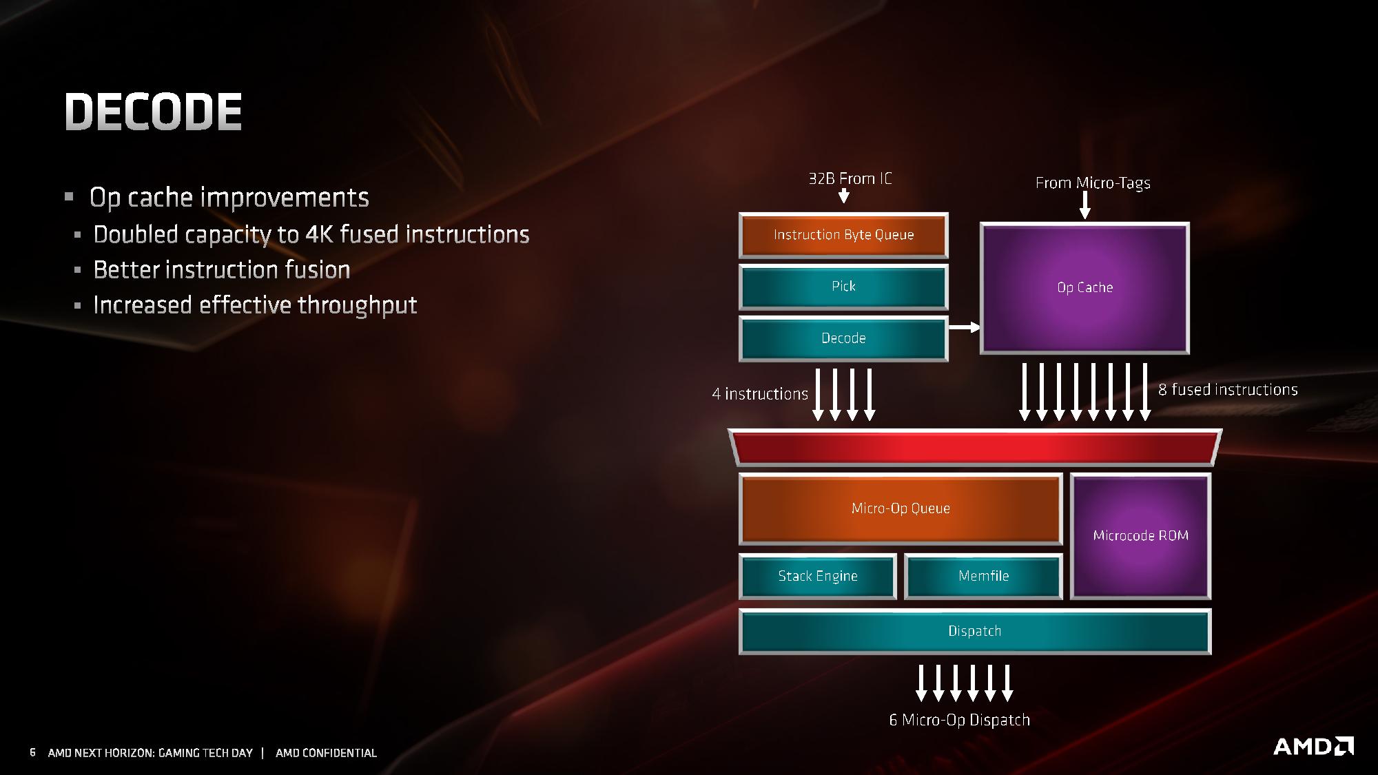
What makes the 4K entry more impressive is when we compare it to the competition. In Intel’s Skylake family, the micro-op cache in those cores are only 1.5K entry. Intel increased the size by 50% for Ice Lake to 2.25K, but that core is coming to mobile platforms later this year and perhaps to servers next year. By comparison AMD’s Zen 2 core will cover the gamut from consumer to enterprise. Also at this time we can compare it to Arm’s A77 CPU micro-op cache, which is 1.5K entry, however that cache is Arm’s first micro-op cache design for a core.
The decoders in Zen 2 stay the same, we still have access to four complex decoders (compared to Intel’s 1 complex + 4 simple decoders), and decoded instructions are cached into the micro-op cache as well as dispatched into the micro-op queue.
AMD has also stated that it has improved its micro-op fusion algorithm, although did not go into detail as to how this affects performance. Current micro-op fusion conversion is already pretty good, so it would be interesting to see what AMD have done here. Compared to Zen and Zen+, based on the support for AVX2, it does mean that the decoder doesn’t need to crack an AVX2 instruction into two micro-ops: AVX2 is now a single micro-op through the pipeline.
Going beyond the decoders, the micro-op queue and dispatch can feed six micro-ops per cycle into the schedulers. This is slightly imbalanced however, as AMD has independent integer and floating point schedulers: the integer scheduler can accept six micro-ops per cycle, whereas the floating point scheduler can only accept four. The dispatch can simultaneously send micro-ops to both at the same time however.


216 Comments
View All Comments
Smell This - Sunday, June 16, 2019 - link
AND ...
it might be 12- to 16 IF links or, another substrate ?
Targon - Thursday, June 13, 2019 - link
Epyc and Ryzen CCX units are TSMC, the true CPU cores. The I/O unit is the only part that comes from Global Foundries, and is probably at TSMC just to satisfy the contracts currently in place.YukaKun - Monday, June 10, 2019 - link
"Users focused on performance will love the new 16-core Ryzen 9 3950X, while the processor seems nice an efficient at 65W, so it will be interesting so see what happens at lower power."Shouldn't that be 105W?
And great read as usual.
Cheers!
jjj - Monday, June 10, 2019 - link
The big problem with this platform is that ST perf per dollar gains are from zero to minimal, depending on SKU.They give us around 20% ST gains (IPC+clocks) but at a cost. Would rather have 10-15% gains for free than to pay for 20%. Pretty much all SKUs need a price drop to become exciting, some about 50$, some a bit less and the 16 cores a lot more.
Got to wonder about memory BW with the 16 cores. 2 channels with 8 cores is one thing but at 16 cores, it might become a limiting factor here and there.
Threska - Tuesday, June 11, 2019 - link
That could be said of any processor. "Yeah, drop the price of whatever it is and we'll love you for it." Improvements cost, just like DVD's costed more than VHS.jjj - Tuesday, June 11, 2019 - link
In the semi business the entire point is to offer significantly more perf per dollar every year. That's what Moore's Law was, 2x the perf at same price every 2 years. Now progress is slower but consumers aren't getting anything anymore.And in pretty much all tech driven areas, products become better every year, even cars. When there is no innovation, it means that the market is dysfunctional. AMD certainly does not innovate here, except on the balance sheet. Innovation means that you get better value and that is missing here. TSMC gives them more perf per dollar, they have additional gains from packaging but those gains do not trickle down to us. At the end of the day even Intel tries to offer 10-15% perf per dollar gains every cycle.
AlyxSharkBite - Tuesday, June 11, 2019 - link
That’s not Moore’s Law at all. It stated that the number of transistors would double. Also it’s been dead a whileSandy bridge 4c 1.16b
Coffee lake 4c is 2.1b (can’t compare the 6c or 8c)
And that’s a lot more than 2 years.
mode_13h - Tuesday, June 11, 2019 - link
Yeah, but those two chips occupy different market segments. So, you should compare Sandybridge i7 vs. Coffelake i7.Teutorix - Tuesday, June 11, 2019 - link
The number of transistors in an IC, not the number of transistors per CPU core. This is an important distinction since a CPU core in Moore's day had very little in it besides registers and an ALU. They didn't integrate FPUs until relatively recently.It's about overall transistor density, nothing more. You absolutely can compare an 8c to a 4c chip, because they are both a single IC.
An 8 core coffee lake chip is 20% smaller than a quad core sandy bridge chip. That's double the CPU cores, double the GPU cores, with probably a massive increase in the transistors/core also.
Moore's law had a minor slowdown with intel stuck at 14nm but its not dead.
Wilco1 - Tuesday, June 11, 2019 - link
Moore's Law is actually accelerating. Just not at Intel. See https://en.wikipedia.org/wiki/Transistor_count - the largest chips now have ~20 Billion transistors, and with 7nm and 5nm it looks like we're getting some more doublings soon.