AMD Rome Second Generation EPYC Review: 2x 64-core Benchmarked
by Johan De Gelas on August 7, 2019 7:00 PM ESTPCIe 4.0
As the first commerical x86 server CPU supporting PCIe 4.0, the I/O capabilities of second generation EPYC servers are top of the class. One PCIe 4.0 x16 offers up to 32 GB/s in both direction, so each socket offers up to 256 GB/s in both directions, for a full 128 PCIe 4.0 lanes per CPU.

Each CPU has 8 x16 PCIe 4.0 links available which can be split up among up to 8 devices per PCIe root, as shown above. There is also full PCIe peer-to-peer support both within a single socket and across sockets.
With the previous generation, in order to enable a dual socket configuration, 64 PCIe lanes from each CPU were used to link them together. For EPYC, AMD still allows for 64 PCIe lanes to be used, but these are PCIe 4.0 lanes now. There is also another feature that AMD has here - socket-to-socket IF link bandwidth management - which allows OEM partners to design dual-socket systems with less socket-to-socket bandwidth and more PCIe lanes if needed.
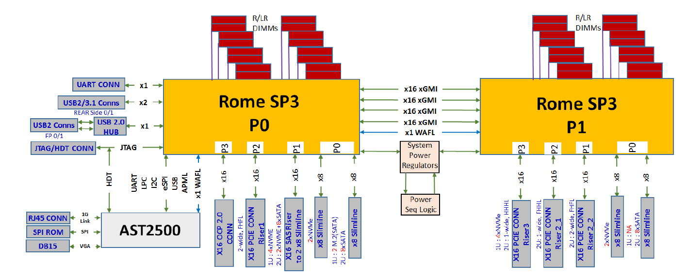
We also learned that there are in fact 129 PCIe 4.0 lanes on each CPU. On each CPU there is one extra PCIe lane for the BMC (the chip that controls the server). Considering we are living in the age of AI acceleration, the EPYC 7002 servers will be great as hosts for quite a few GPUs or TPUs. Density has never looked so fun.


180 Comments
View All Comments
ET - Thursday, August 8, 2019 - link
I found the EPYC 7262 the most interesting SKU. By L3 cache size, that would be 4 chiplets, each offering only 2 cores. From the specs it looks like AMD has no shortage of 4 core chiplets, but I didn't expect 2 core chiplets.Rudde - Friday, August 9, 2019 - link
L3 cache is shared inside a CCX (4 cores), which suggests that every CCX has only one core available, but 16MB of L3 cache. I.e. every core has private L3 cache.colonelclaw - Thursday, August 8, 2019 - link
But can it serve Crysis Battle Royale?shing3232 - Thursday, August 8, 2019 - link
I am pretty sure it can lolBigMamaInHouse - Thursday, August 8, 2019 - link
@ Johan De Gelas will u test @240W TDP config?JohanAnandtech - Thursday, August 8, 2019 - link
Elaborate your interest in that, as it is only tad higher than the official 225W TDP?BigMamaInHouse - Thursday, August 8, 2019 - link
AMD is offering 225W/240W TDP option in bios to it's customers and lets them to decide if to go with better cooling and use 240W or stay at 225W, even though it looks small increase- in reality it should offer almost 10% more power headroom to the CPU chiplets -if you consider that the 225W is including ~55W for I/O die, so extra 15W for the chiplets alone should offer nice bump in clocks.Gondalf - Thursday, August 8, 2019 - link
Strange.....the article forgot Cooper Lake, out in Q4 this year and at major customers (for revenue) from at least two quarters. Same applies to Ice Lake SP that is in evaluation to OEMs right now.From the article looks like Intel is sleeping, but it is not at all. Ummm maybe Intel is snobbing some guys here not giving samples to test?? or informations to share??
Bet Intel have to argue about the test suite or about compiler settings.........
JohanAnandtech - Thursday, August 8, 2019 - link
Because Cooper Lake is still "warmed up Skylake" (unless I missed something). AFAIK it is Cascade Lake with 8 mem channels - so the 56-core socketed will probably be still in the 350-400W TDP range. So the SPEC benchmarks will look better, but getting that kind of server running inside your datacenter does not look very attractive: complex and thus expensive boards, high cooling and power distribution required. Looks like a chip that wins back benchmarks, but is too much hassle to roll out in high quantities.Null666666 - Friday, August 9, 2019 - link
Wondering when 4-8 socket ice lake is due.