AMD Rome Second Generation EPYC Review: 2x 64-core Benchmarked
by Johan De Gelas on August 7, 2019 7:00 PM ESTBetter Core in Zen 2
Just in case you have missed it, in our microarchitecture analysis article Ian has explained in great detail why AMD claims that its new Zen2 is significantly better architecture than Zen1:
- a different second-stage branch predictor, known as a TAGE predictor
- doubling of the micro-op cache
- doubling of the L3 cache
- increase in integer resources
- increase in load/store resources
- support for two AVX-256 instructions per cycle (instead of having to combine two 128 bit units).
All of these on-paper improvements show that AMD is attacking its key markets in both consumer and enterprise performance. With the extra compute and promised efficiency, we can surmise that AMD has the ambition to take the high-performance market back too. Unlike the Xeon, the 2nd gen EPYC does not declare lower clocks when running AVX2 - instead it runs on a power aware scheduler that supplies as much frequency as possible within the power constraints of the platform.
Users might question, especially with Intel so embedded in high performance and machine learning, why AMD hasn't gone with an AVX-512 design? As a snap back to the incumbent market leader, AMD has stated that not all 'routines can be parallelized to that degree', as well as a very clear signal that 'it is not a good use of our silicon budget'. I do believe that we may require pistols at dawn. Nonetheless, it will be interesting how each company approaches vector parallelisation as new generations of hardware come out. But as it stands, AMD is pumping its FP performance without going full-on AVX-512.
In response to AMD's claims of an overall 15% IPC increase for Zen 2, we saw these results borne out of our analysis of Zen 2 in the consumer processor line, which was released last month. In our analysis, Andrei checked and found that it is indeed 15-17% faster. Along with the performance improvements, there have been also security hardening updates, improved virtualization support, and new but proprietary instructions for cache and memory bandwidth Quality of Service (QoS). (The QoS features seem very similar to what Intel has introduced in Broadwell/Xeon E5 version 4 and Skylake - AMD is catching up in that area).
Rome Layout: Simple Makes It a Lot Easier
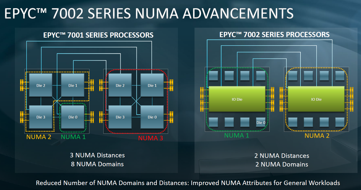
When we analyzed AMD's first generation of EPYC, one of the big disadvantages was the complexity. AMD had built its 32-core Naples processors by enabling four 8-core silicon dies, and attaching each one to two memory channels, resulting in a non-uniform memory architecutre (NUMA). Due to this 'quad NUMA' layout, a number of applications saw quite a few NUMA balancing issues. This happened in almost every OS, and in some cases we saw reports that system administrators and others had to do quite a bit optimization work to get the best performance out of the EPYC 7001 series.
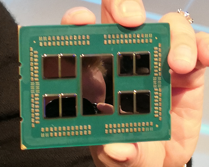
The New 2nd Gen EPYC, Rome, has solved this. The CPU design implements a central I/O hub through which all communications off-chip occur. The full design uses eight core chiplets, called Core Complex Dies (CCDs), with one central die for I/O, called the I/O Die (IOD). All of the CCDs communicate with this this central I/O hub through dedicated high-speed Infinity Fabric (IF) links, and through this the cores can communicate to the DRAM and PCIe lanes contained within, or other cores.
The CCDs consist of two four-core Core CompleXes (1 CCD = 2 CCX). Each CCX consist of a four cores and 16 MB of L3 cache, which are at the heart of Rome. The top 64-core Rome processors overall have 16 CCX, and those CCX can only communicate with each other over the central I/O die. There is no inter-chiplet CCD communication.

This is what this diagram shows. On the left we have Naples, first Gen EPYC, which uses four Zepellin dies each connected to the other with an IF link. On the right is Rome, with eight CCDs in green around the outside, and a centralized IO die in the middle with the DDR and PCIe interfaces.
As Ian reported, while the CCDs are made at TSMC, using its latest 7 nm process technology. The IO die by contrast is built on GlobalFoundries' 14nm process. Since I/O circuitry, especially when compared to caching/processing and logic circuitry, is notoriously hard to scale down to smaller process nodes, AMD is being clever here and using a very mature process technology to help improve time to market, and definitely has advantages.
This topology is clearly visible when you take off the hood.
Main advantage is that the 2nd Gen 'EPYC 7002' family is much easier to understand and optimize for, especially from a software point of view, compared to Naples. Ultimately each processor only has one memory latency environment, as each core has the same latency to speak to all eight memory channels simultanously - this is compared to the first generation Naples, which had two NUMA regions per CPU due to direct attached memory.
As seen in the image below, this means that in a dual socket setup, a Naples processor will act like a traditional NUMA environment that most software engineers are familiar with.
Ultimately the only other way to do this is with a large monolithic die, which for smaller process nodes is becoming less palatable when it comes to yields and pricing. In that respect, AMD has a significant advantage in being able to develop small 7nm silicon with high yields and also provide a substantial advantage when it comes to binning for frequency.
How a system sees the new NUMA environment is quite interesting. For the Naples EPYC 7001 CPUs, this was rather complicated in a dual socket setup:
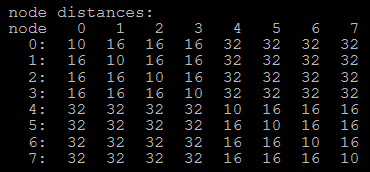
Here each number shows the 'weighting' given to the delay to access each of the other NUMA domains. Within the same domain, the weighting is light at only 10, but then a NUMA domain on the same chip was given a 16. Jumping off the chip bumped this up to 32.
This changed significantly on Rome EPYC 7002:

Although there are situations where the EPYC 7001 CPUs communicated faster, but the fact that the topology is much simpler from the software point of view is worth a lot. It makes getting good performance out of the chip much easier for everyone that has to used it, which will save a lot of money in Enterprise, but also help accelerate adoption.


180 Comments
View All Comments
Kevin G - Wednesday, August 7, 2019 - link
Clock speeds. AMD is being very aggressive on clocks here but the Ryzen 3000 series were still higher. I would expect new Threadripper chips to clock closer to their Ryzen 3000 cousins.AMD *might* differentiate Threadripper by cache amounts. While the CPU cores work, they may end up binning Threadripper based upon the amount of cache that wouldn't pass memory tests.
Last thing would be price. The low end Epyc chips are not that expensive but suffer from low cores/low clocks. Threadripper can offer more for those prices.
quorm - Wednesday, August 7, 2019 - link
Here's hoping we see a 16 core threadripper with a 4ghz base clock.azfacea - Wednesday, August 7, 2019 - link
half memory channels. half pcie lanes. also i think with epyc AMD spends more on support and system development. i can see 48c 64c threadripper coming 30-40% lower and not affecting epyctwtech - Wednesday, August 7, 2019 - link
If they gimp the memory access again, it mostly defeats the purpose of TR as a workstation chip. You'd want an Epyc anyway.quorm - Wednesday, August 7, 2019 - link
Well, on the plus side, the i/o die should solve the asymmetric memory access problem.ikjadoon - Wednesday, August 7, 2019 - link
Stunning.aryonoco - Wednesday, August 7, 2019 - link
Between 50% to 100% higher performance while costing between 40% to 50% less. Stunning!I remember the sad days of Opteron in 2012 and 2013. If you'd told me that by the end of the decade AMD would be in this position, I'd have wanted to know what you're on.
Everyone at AMD deserves a massive cheer, from the technical and engineering team all the way to Lisa Su, who is redefining what "execution" means.
Also thanks for the testing Johan, I can imagine testing this server at home with Europe's recent heatwave would have not been fun. Good to see you writing frequently for AT again, and looking forward to more of your real world benchmarks.
twtech - Wednesday, August 7, 2019 - link
It's as much about Intel having dropped the ball over the past few years as it is about AMD's execution.According to Intel's old roadmaps, they ought to be transitioning past 10nm on to 7nm by now, and AMD's recent releases in that environment would have seemed far less impressive.
deltaFx2 - Wednesday, August 7, 2019 - link
Yeah, except I don't remember anyone saying Intel was going great guns because AMD dropped the ball in the bulldozer era. AMD had great bulldozer roadmaps too, it didn't matter much. If bulldozer had met its design targets maybe Nehalem would not be as impressive... See, nobody ever says that. It's almost like if AMD is doing well, it's not because they did a good job but intel screwed up.Roadmaps are cheap. Anyone can cobble together a powerpoint slide.
Lord of the Bored - Thursday, August 8, 2019 - link
Well, it is a little of both on both sides.Intel's been doing really well in part because AMD bet hard on Bulldozer and it didn't pay out.
Similarly, when AMD's made really good processors but Intel was on their game, it didn't much matter. The Athlon and the P2/3 traded blows in the Megahertz wars, but in the end AMD couldn't actually break Intel because Intel made crooked business deals*backspace* because AMD was great, but not actually BETTER.
The Athlon 64 was legendary because AMD was at the top of their game and Intel was riding THEIR Bulldozer into the ground at the same time. If the Pentium Mobile hadn't existed, thus delaying a Netburst replacement, things would be very different right now.