Hot Chips 31 Live Blogs: Cerebras' 1.2 Trillion Transistor Deep Learning Processor
by Dr. Ian Cutress on August 19, 2019 9:45 PM EST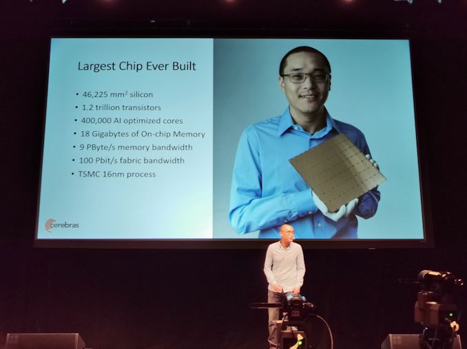
08:49PM EDT - Some of the big news of today is Cerebras announcing its wafer-scale 1.2 trillion transistor solution for deep learning. The talk today goes into detail about the technology.

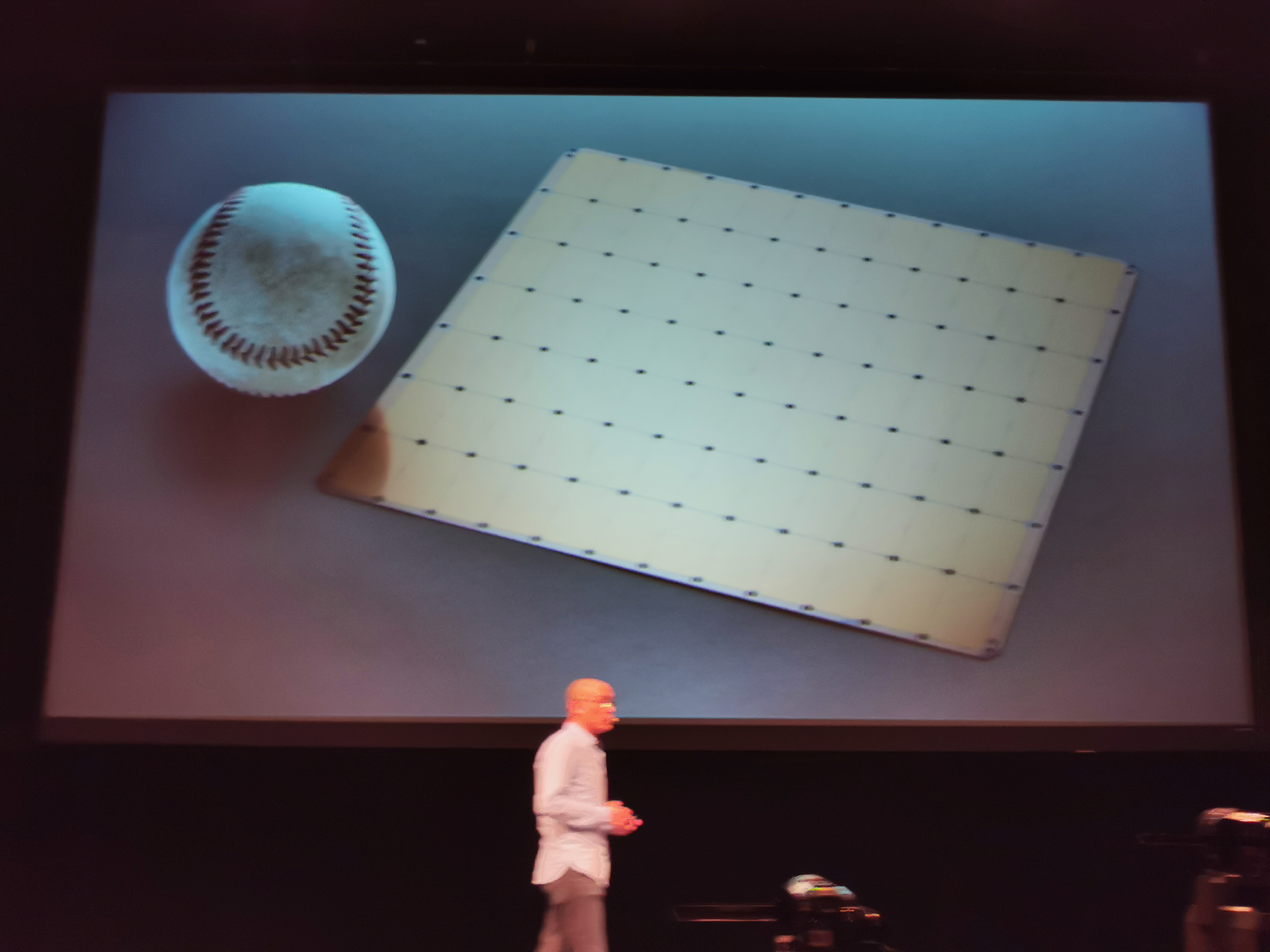
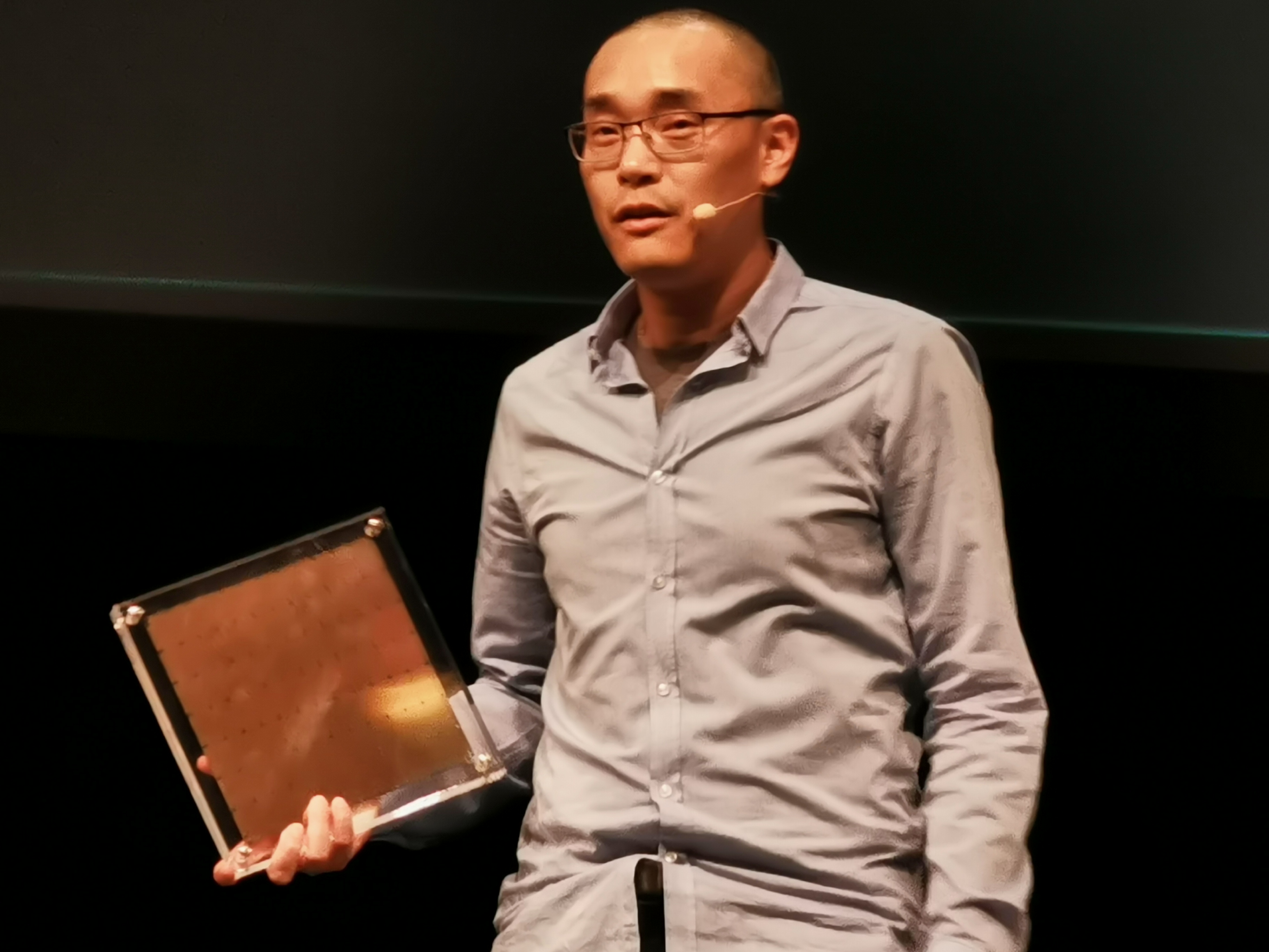
08:51PM EDT - Wafer scale chip, over 46,225 mm2, 1.2 trillion transistors, 400k AI cores, fed by 18GB of on-chip SRAM
08:51PM EDT - TSMC 16nm
08:51PM EDT - 215mm x 215mm - 8.5 inches per side
08:51PM EDT - 56 times larger than the largest GPU today
08:52PM EDT - Built for Deep Learning
08:52PM EDT - DL training is hard (ed: this is an understatement)
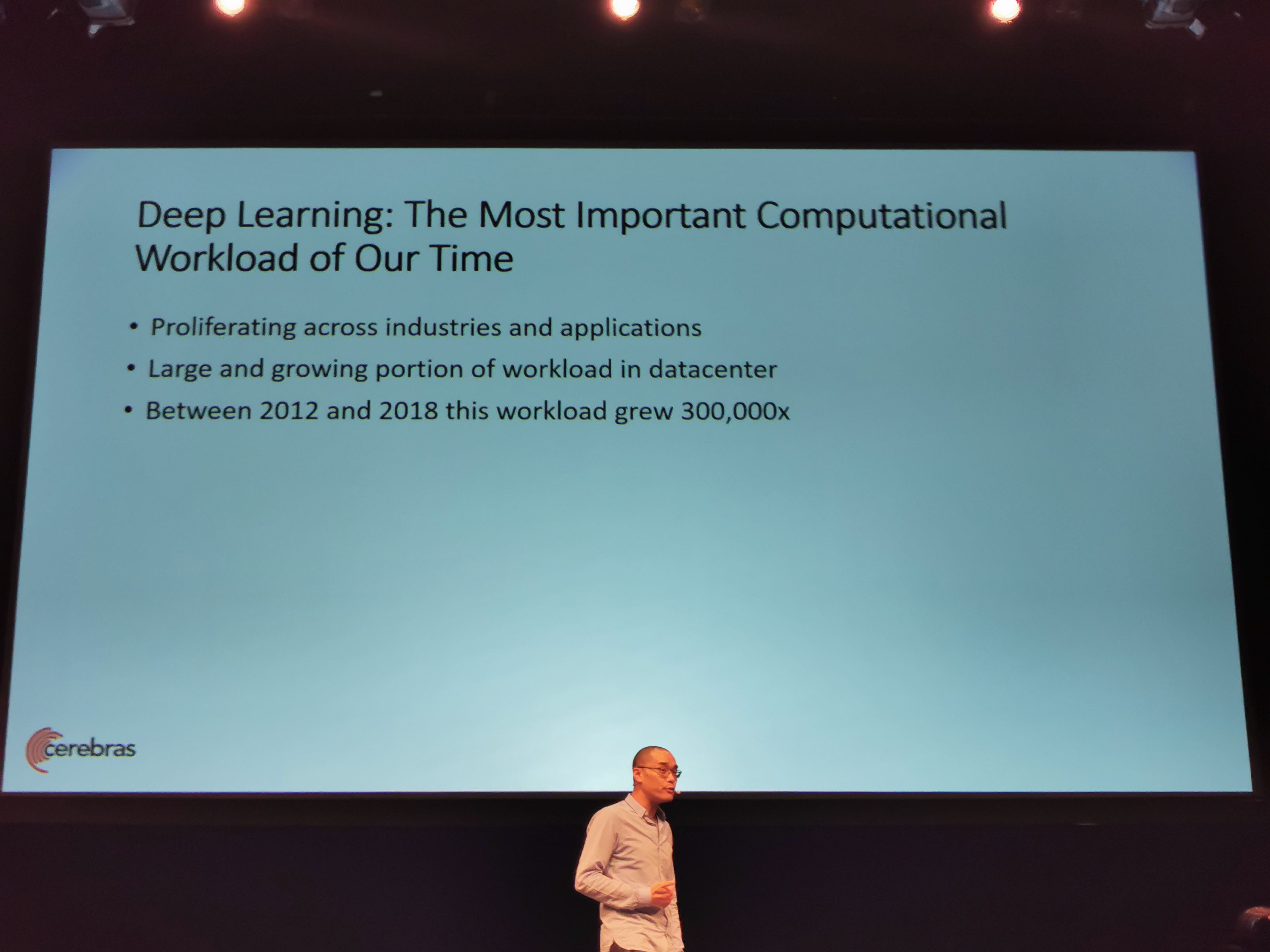
08:52PM EDT - Peta-to-exa scale compute range
08:53PM EDT - The shape of the problem is difficult to scale
08:53PM EDT - Fine grain has a lot of parallelism
08:53PM EDT - Coarse grain is inherently serial
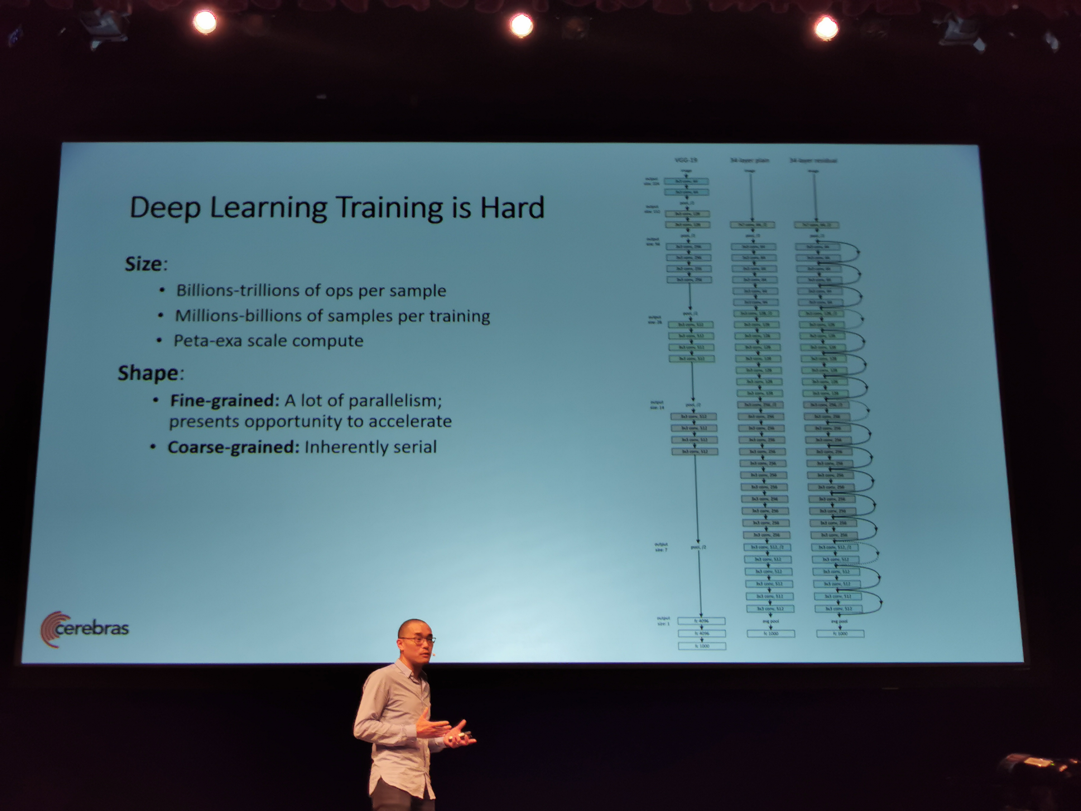
08:53PM EDT - Training is the process of applying small changes, serially
08:53PM EDT - Size and shape of the problem makes training NN really hard
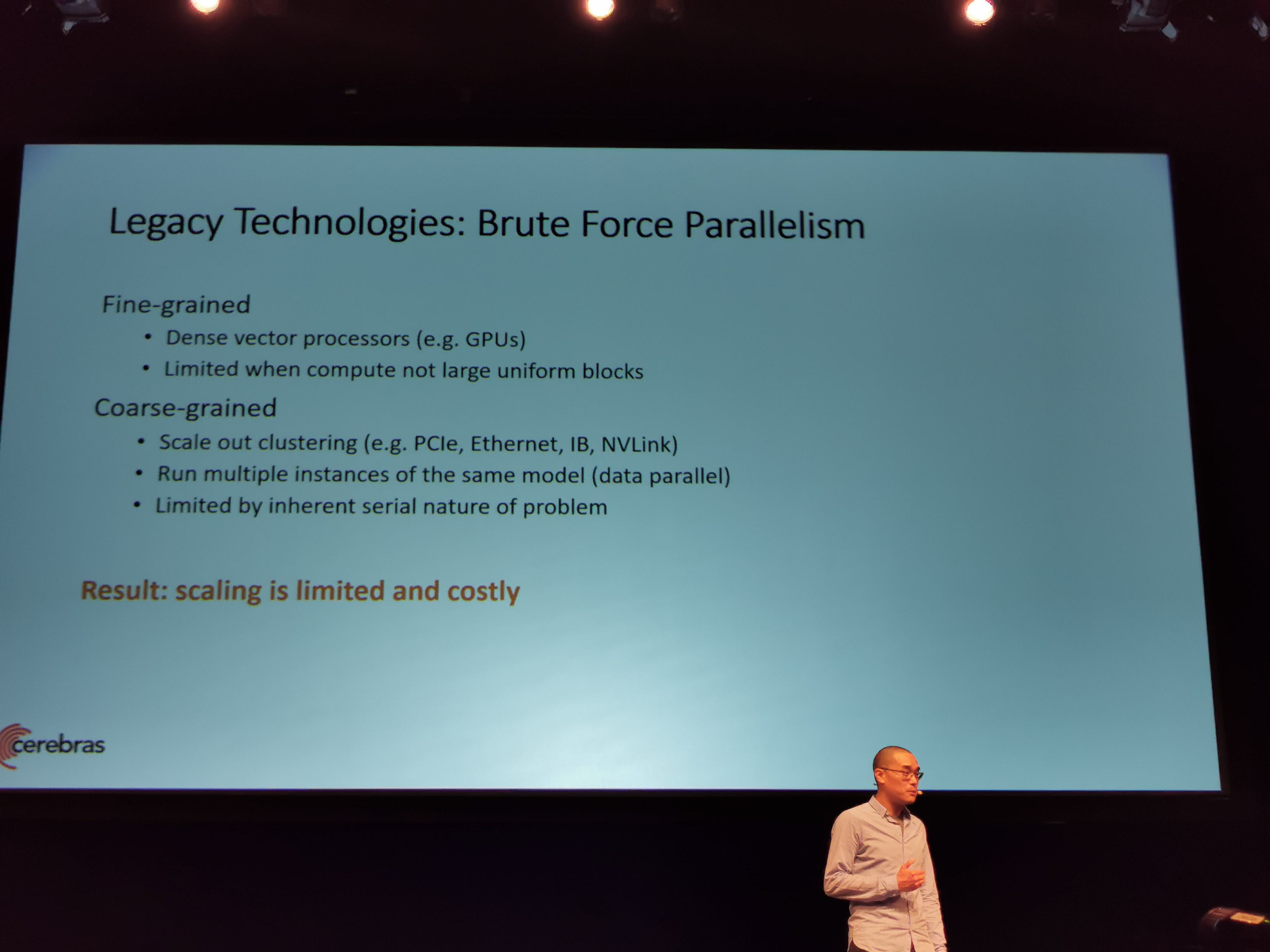
08:53PM EDT - Today we have dense vector compute
08:54PM EDT - For Coarse Grained, require high speed interconnect to run mutliple instances. Still limited
08:54PM EDT - Scaling is limited and costly
08:54PM EDT - Specialized accelerators are the answer
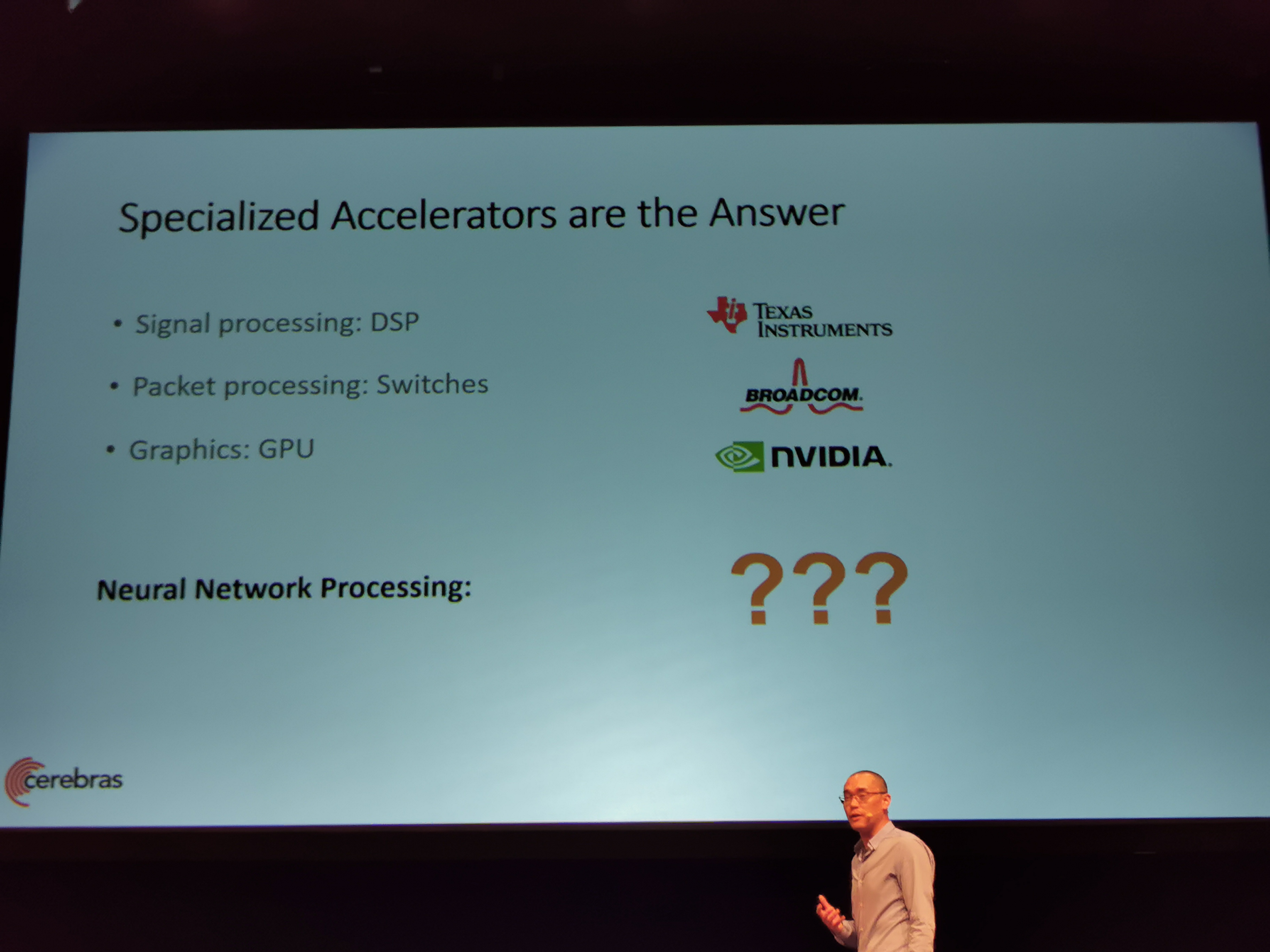
08:55PM EDT - NN: what is the right architecture
08:55PM EDT - Need a core to be optimized for NN primitives
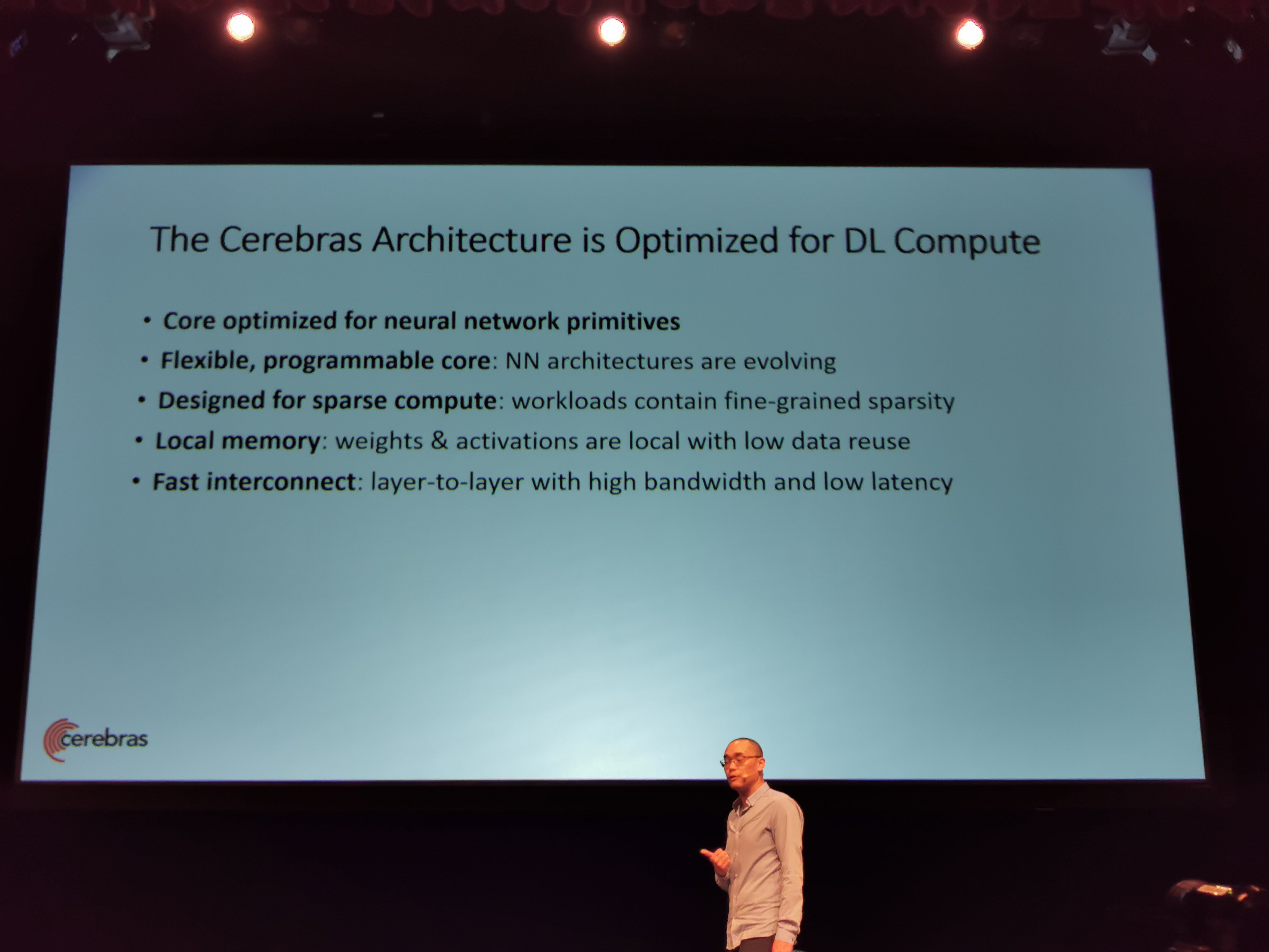
08:55PM EDT - Need a programmable NN core
08:55PM EDT - Needs to do sparse compute fast
08:55PM EDT - Needs fast local memory
08:55PM EDT - All of the cores should be connected with a fast interconnect
08:56PM EDT - Cerebras uses flexible cores. Flexible general ops for control processing
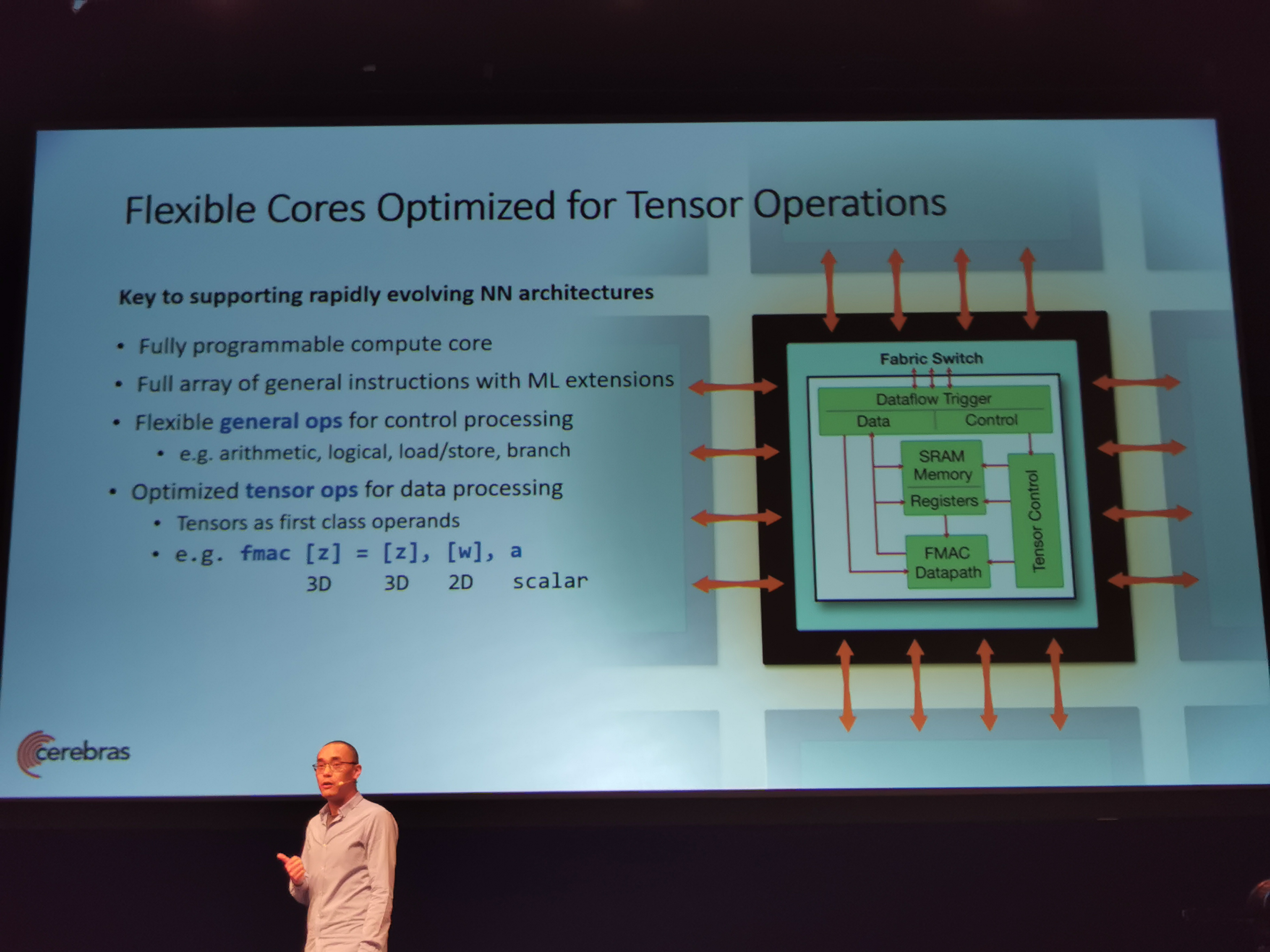
08:56PM EDT - Core should handle tensor operations very efficiency
08:56PM EDT - Forms the bulk fo the compute in any neural network
08:56PM EDT - Tensors as first class operands
08:57PM EDT - fmac native op
08:57PM EDT - NN naturally creates sparse networks
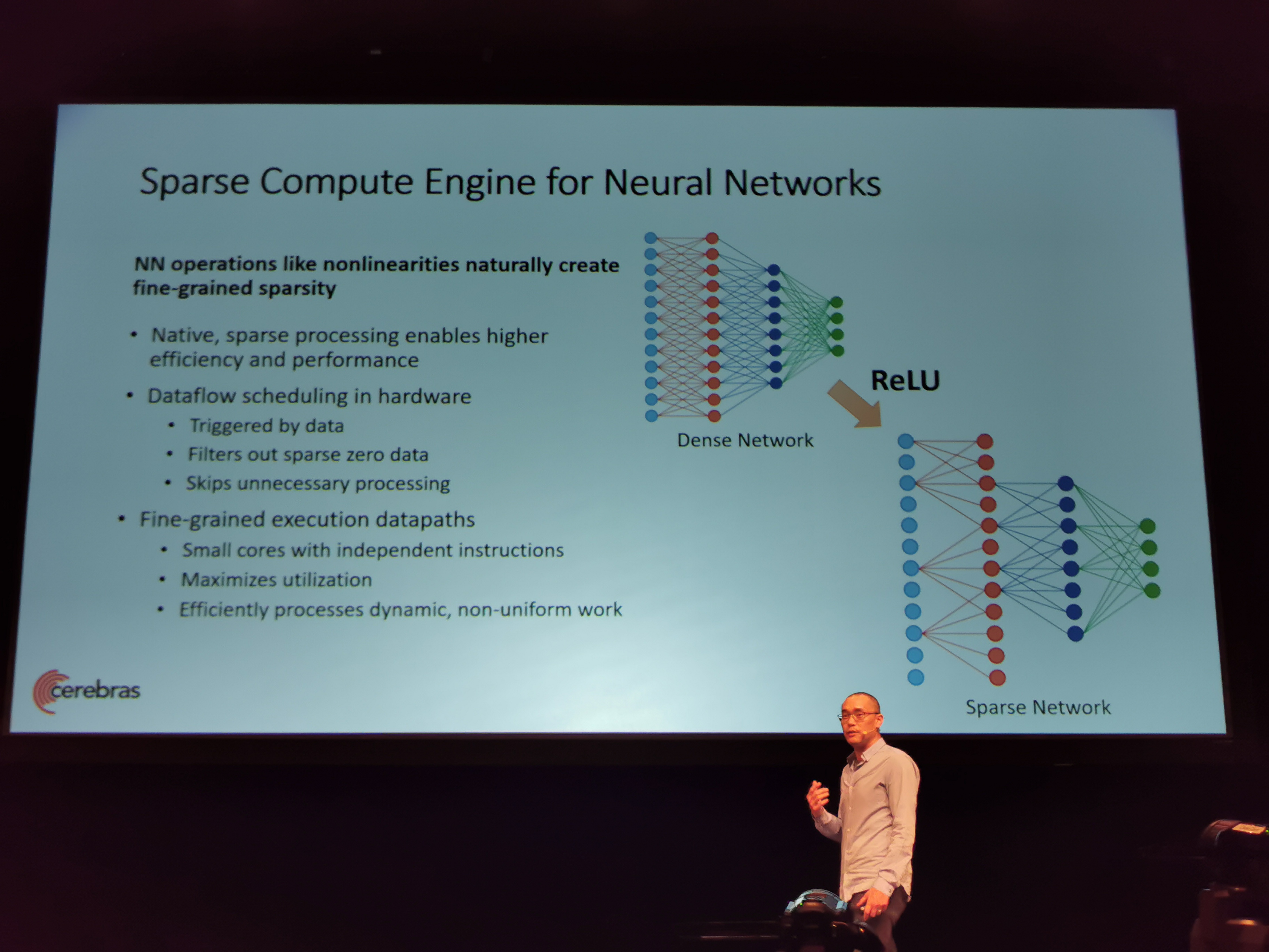
08:58PM EDT - The core has native sparse processing in the hardware with dataflow scheduling
08:58PM EDT - All the compute is triggered by the data
08:58PM EDT - Filters all the sparse zeros, and filters the work
08:58PM EDT - saves the power and energy, and get performance and acceleration by moving onto the next useful work
08:58PM EDT - Enabled because arch has fine-grained execution datapaths
08:58PM EDT - Many small cores with independent instructions
08:59PM EDT - Allows for very non-uniform work
08:59PM EDT - Next is memory
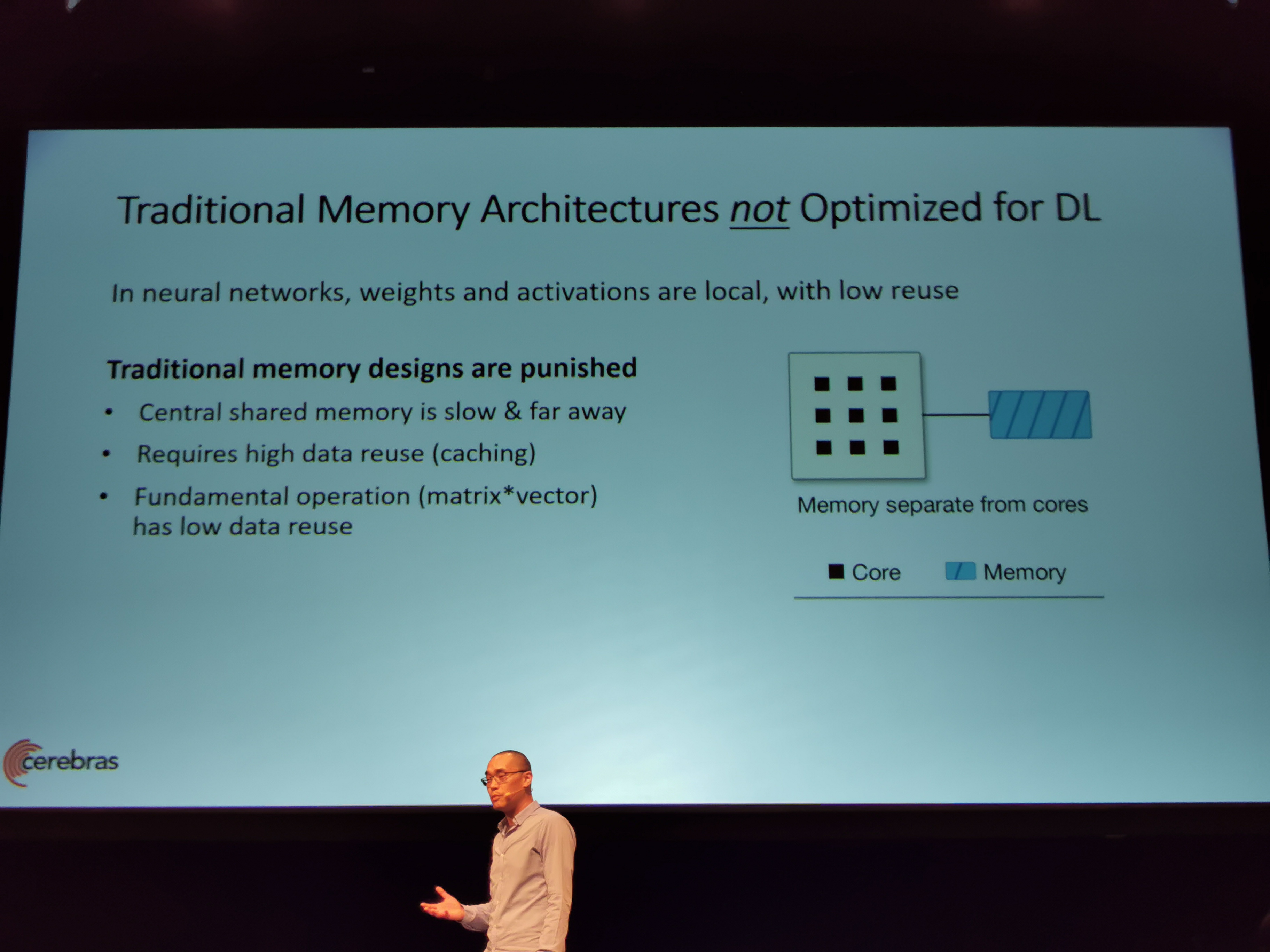
08:59PM EDT - Traditional memory architectures are not optimized for DL
08:59PM EDT - Traditional memory requires high data reuse for performane
09:00PM EDT - Normal matrix multiply has low end data reuse
09:00PM EDT - Translating Mat*Vec into Mat*Mat, but changes the training dynamics
09:00PM EDT - Cerebras has high-perf, fully distributed on-chip SRAM next to the cores
09:01PM EDT - Getting orders of magnitude higher bandwidth
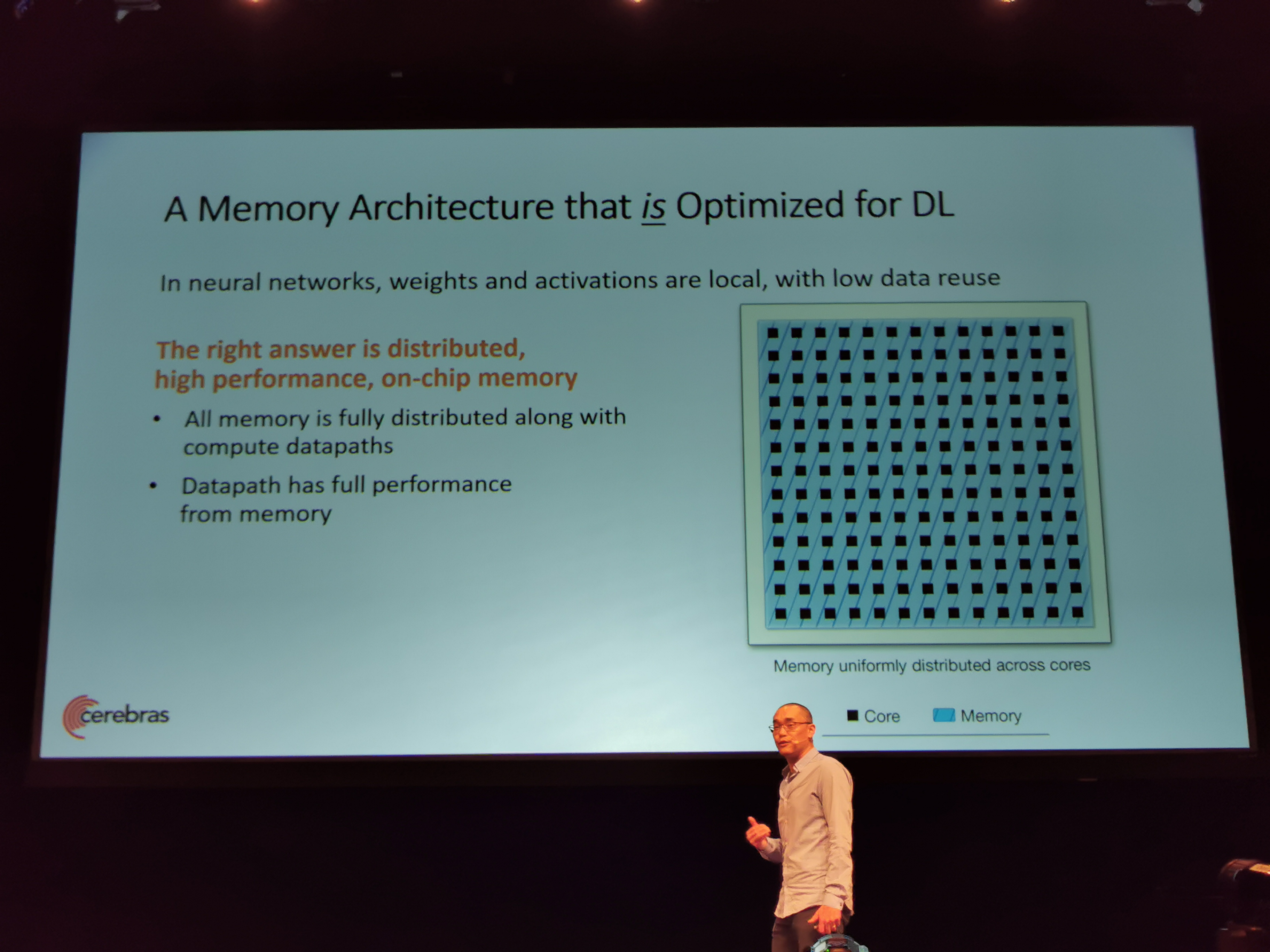
09:01PM EDT - ML can be done the way it wants to be done
09:01PM EDT - High bandwidth, low latency interconnect
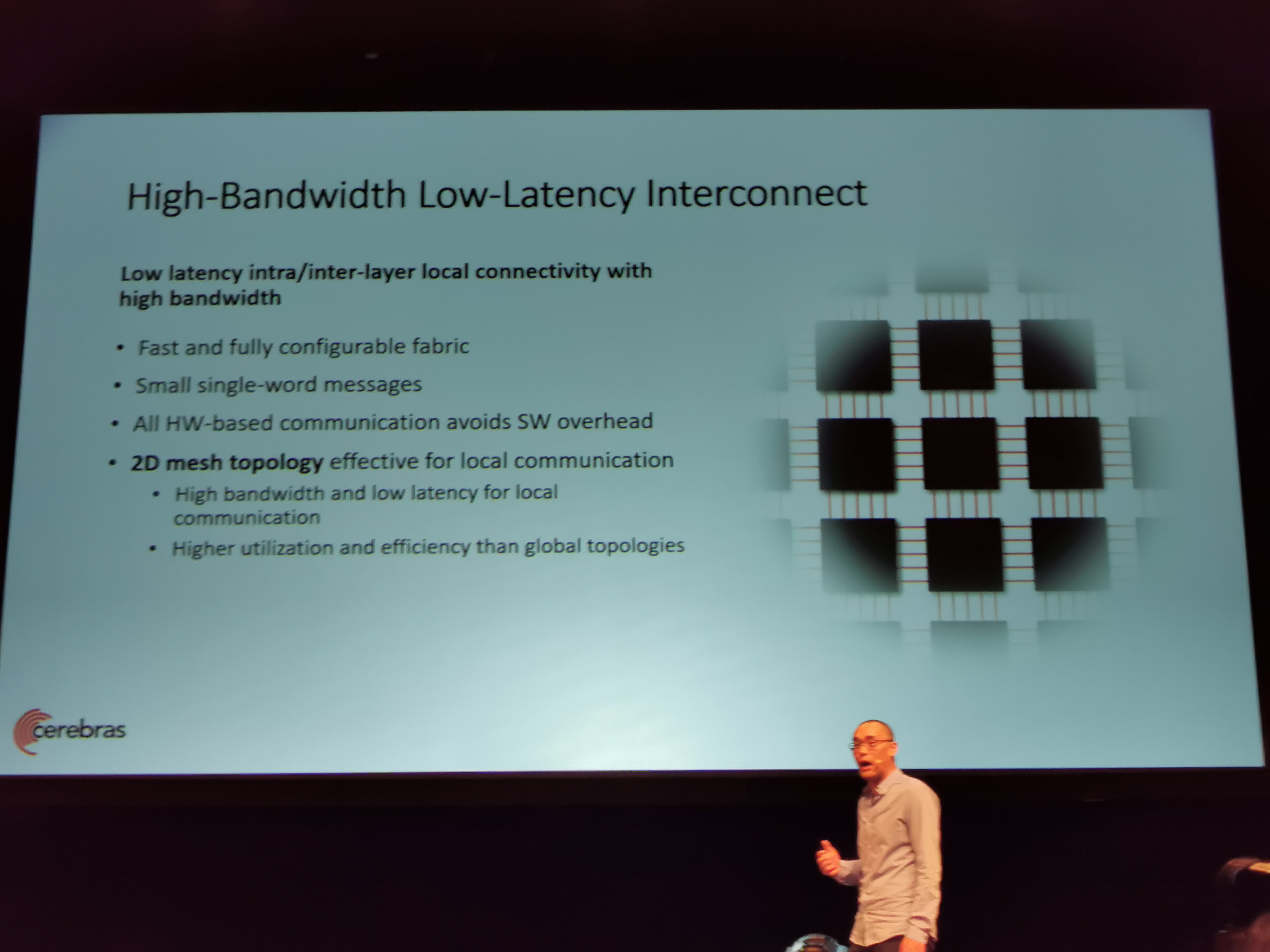
09:01PM EDT - fast and fully configurable fabric
09:01PM EDT - all hw based communication avoicd sw overhead
09:02PM EDT - 2D mesh topology
09:02PM EDT - higher utlization and efficiency than global topologies
09:02PM EDT - Need more than a single die
09:02PM EDT - Solition is a wafer scale
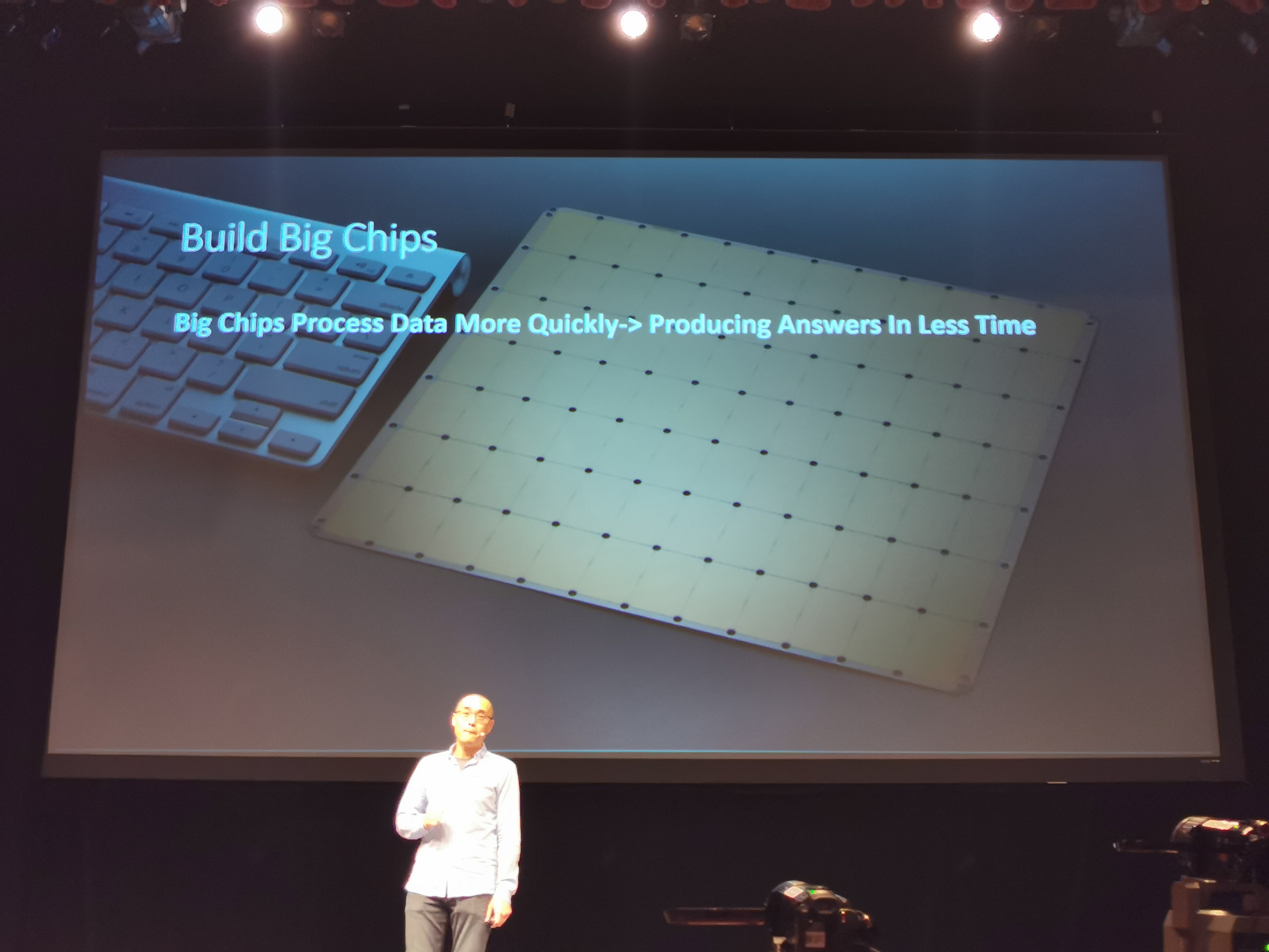
09:03PM EDT - Build Big chips
09:03PM EDT - Cluster scale perf on a single chip
09:03PM EDT - GB of fast memory (SRAM) 1 clock cycle from the core
09:03PM EDT - That's impossible with off-chip memory
09:03PM EDT - Full on-chip interconnect fabric
09:03PM EDT - Model parallel, linear performance scaling
09:04PM EDT - Map the entire neural network onto the chip at once
09:04PM EDT - One instance of NN, don't have to increase batch size to get cluster scale perf
09:04PM EDT - Vastly lower power and less space
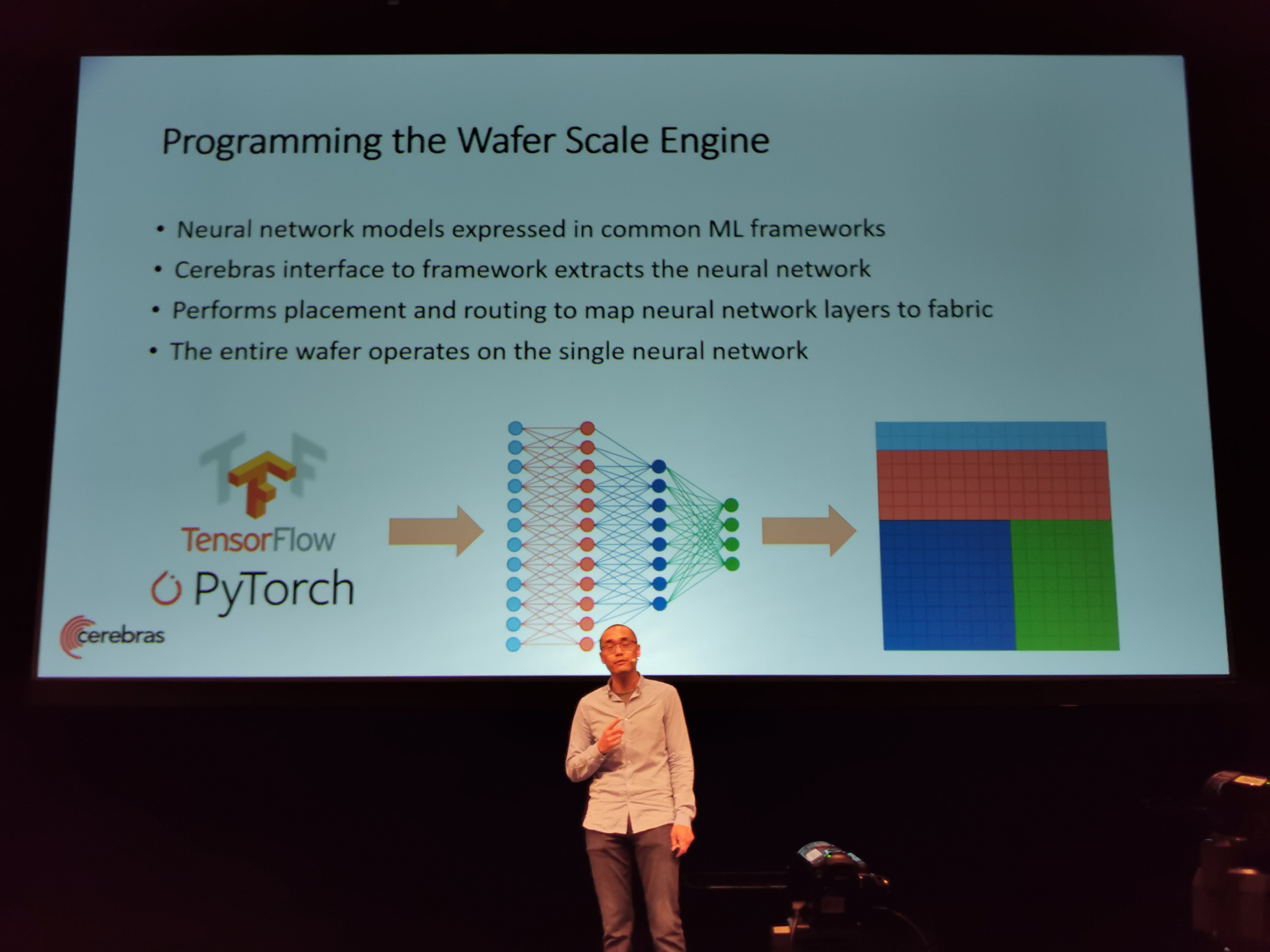
09:04PM EDT - Can use TensorFlow and PyTorch
09:05PM EDT - Performs placing and routing to map neural network layers to fabric
09:05PM EDT - Entire wafer operates on the single neural network
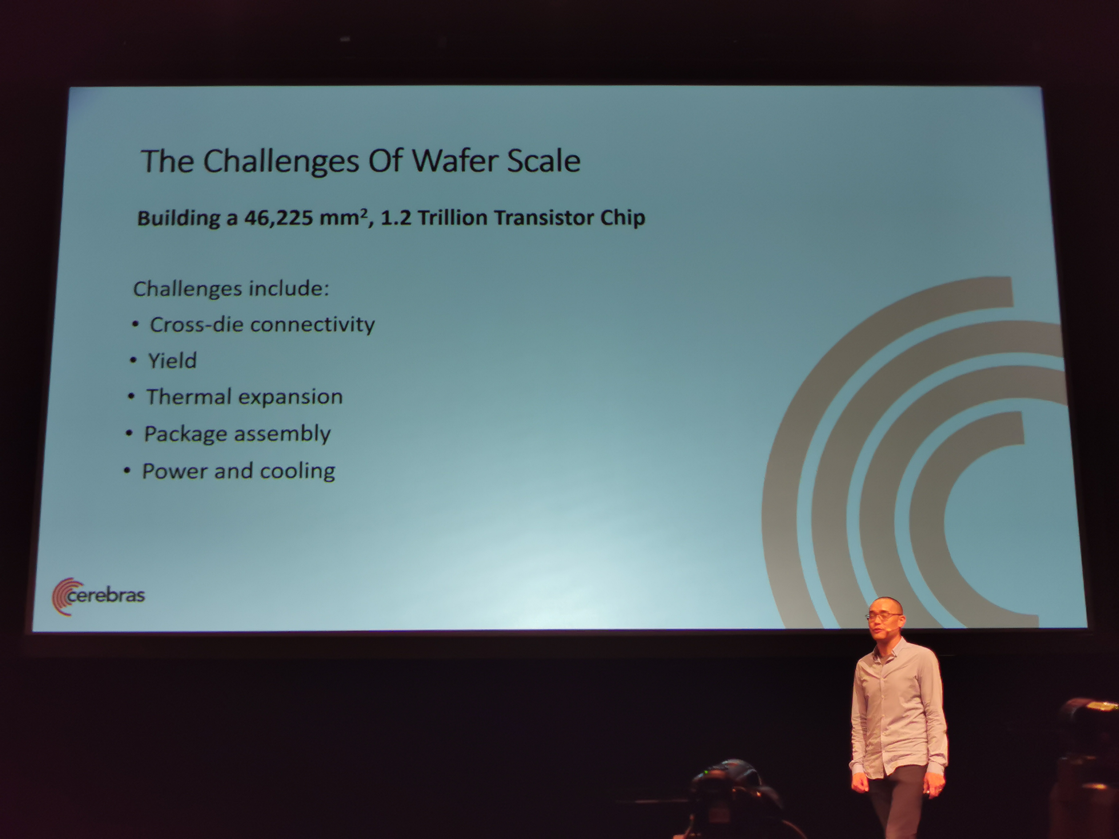
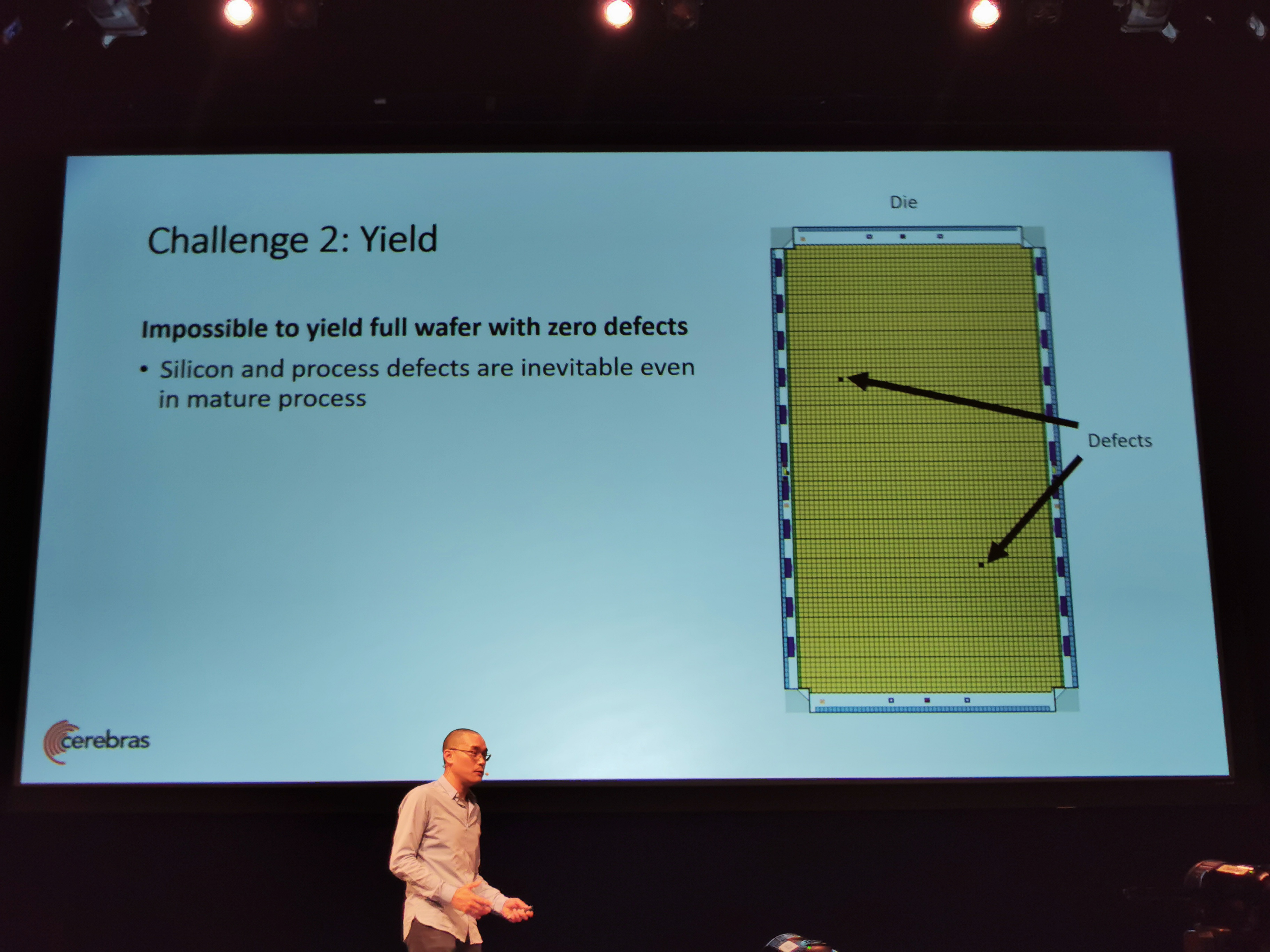
09:05PM EDT - Challenges of wafer scale
09:05PM EDT - Need cross-die connectivity, yield, thermal expansion
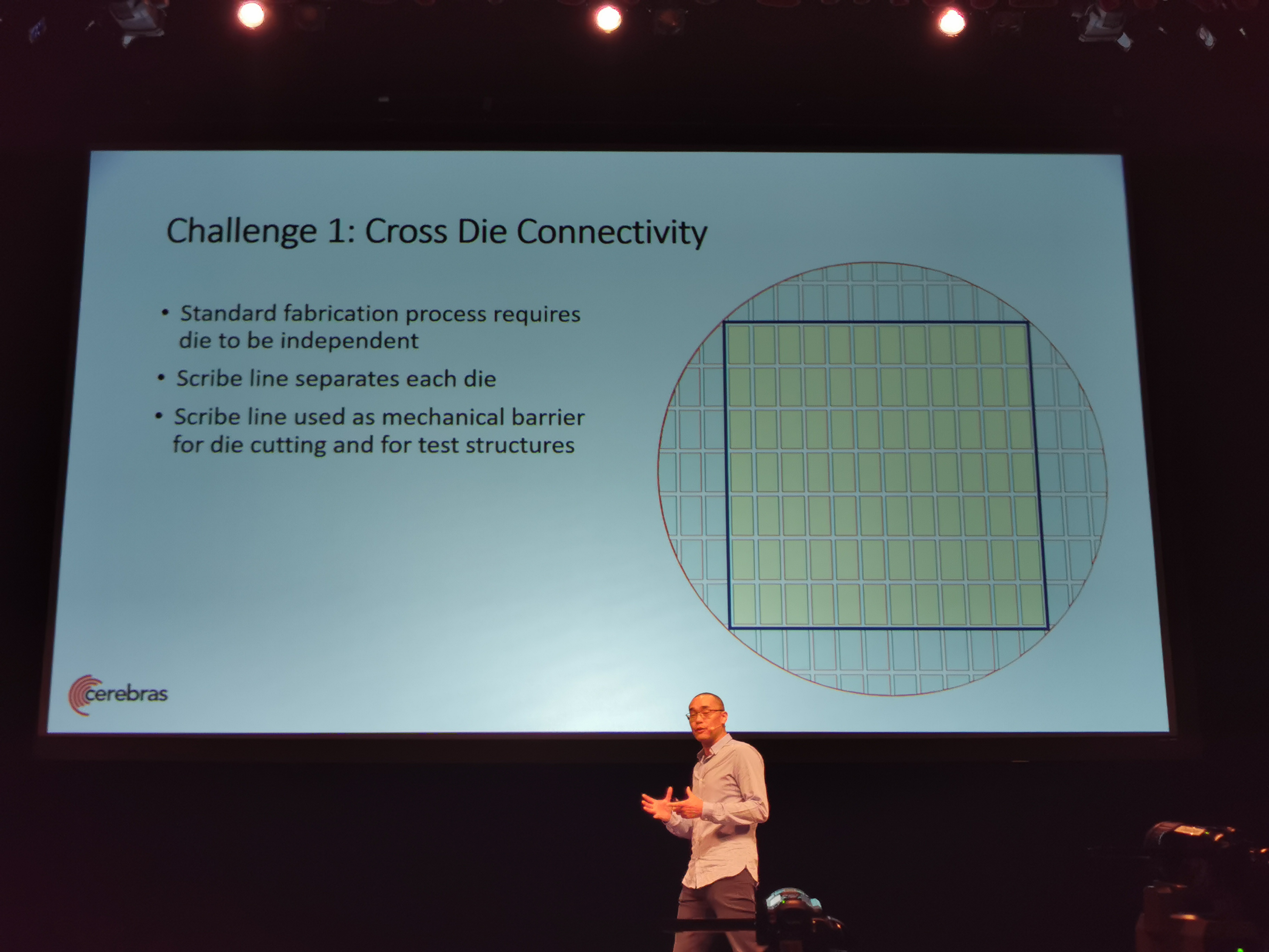
09:06PM EDT - Scribe line separates the die. On top of the scribe line, create wires
09:07PM EDT - Extends 2D mesh fabric across all die
09:07PM EDT - Same connectivity between cores and between die
09:07PM EDT - More efficient than off-chip
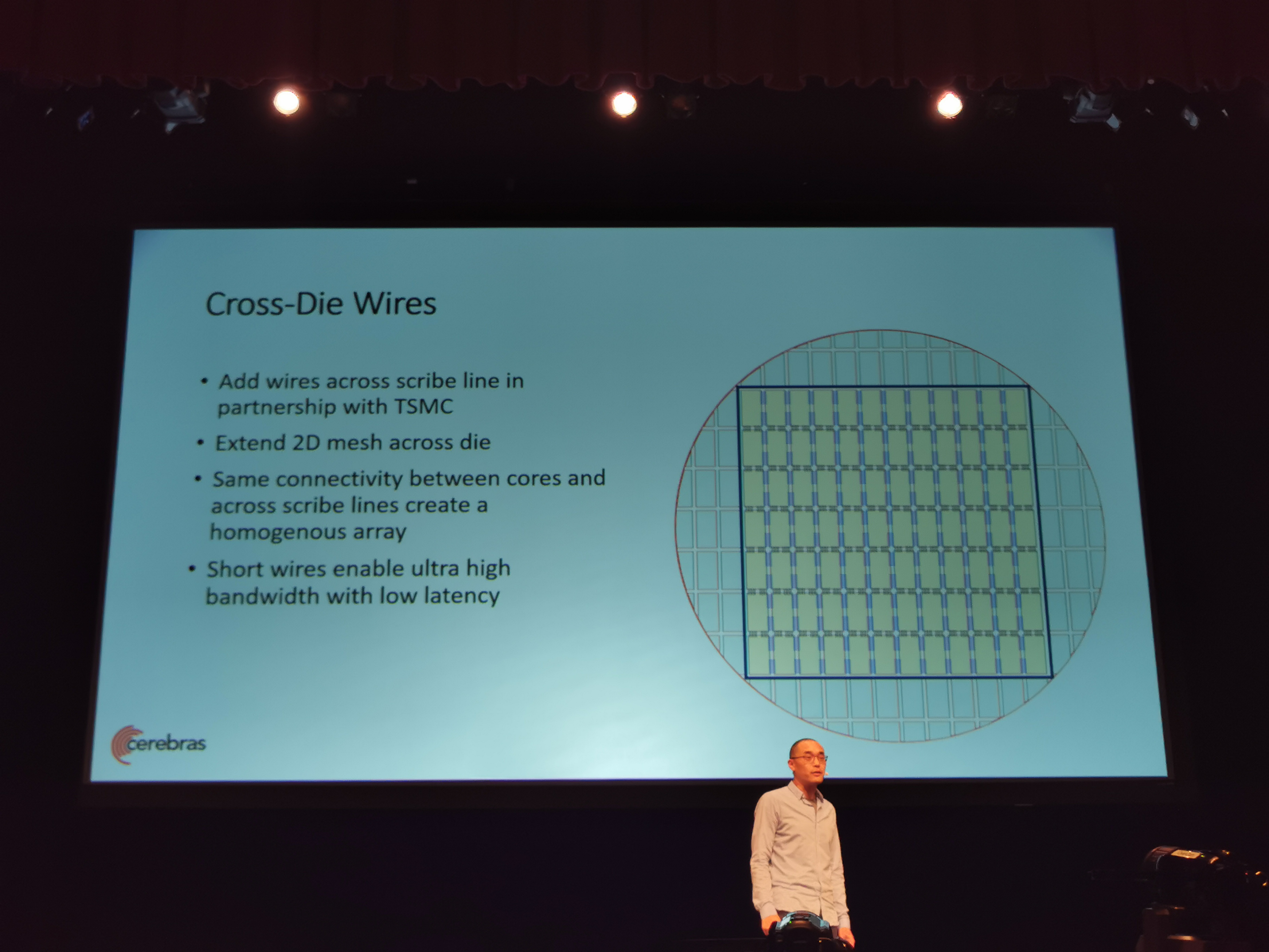
09:07PM EDT - Full BW at the die level
09:08PM EDT - Redundancy helps yield
09:08PM EDT - Redundant cores and redundant fabric links
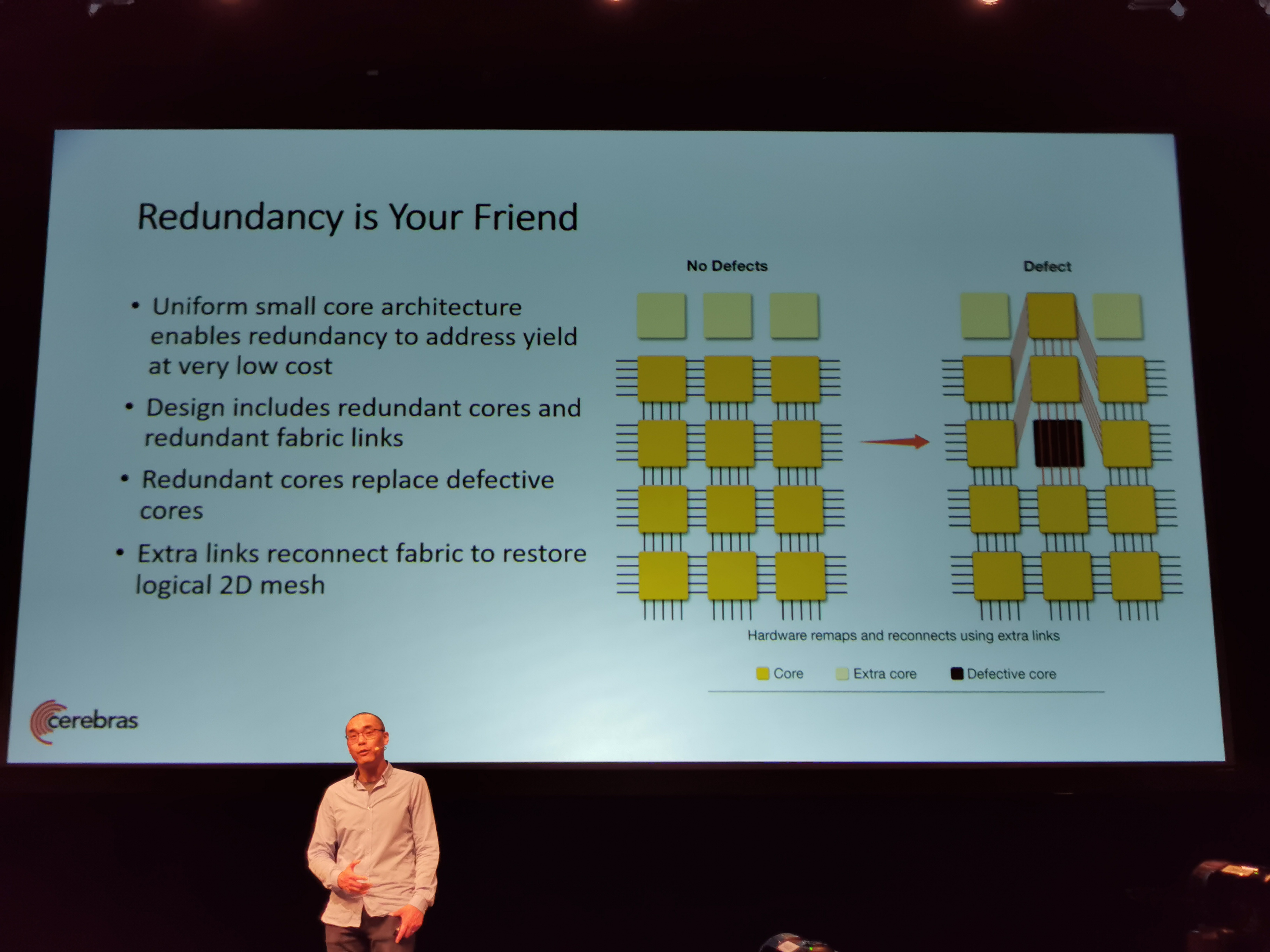
09:08PM EDT - Reconnect the fabric with links
09:08PM EDT - Drive yields high
09:09PM EDT - Transparent to software
09:09PM EDT - Thermal expansion
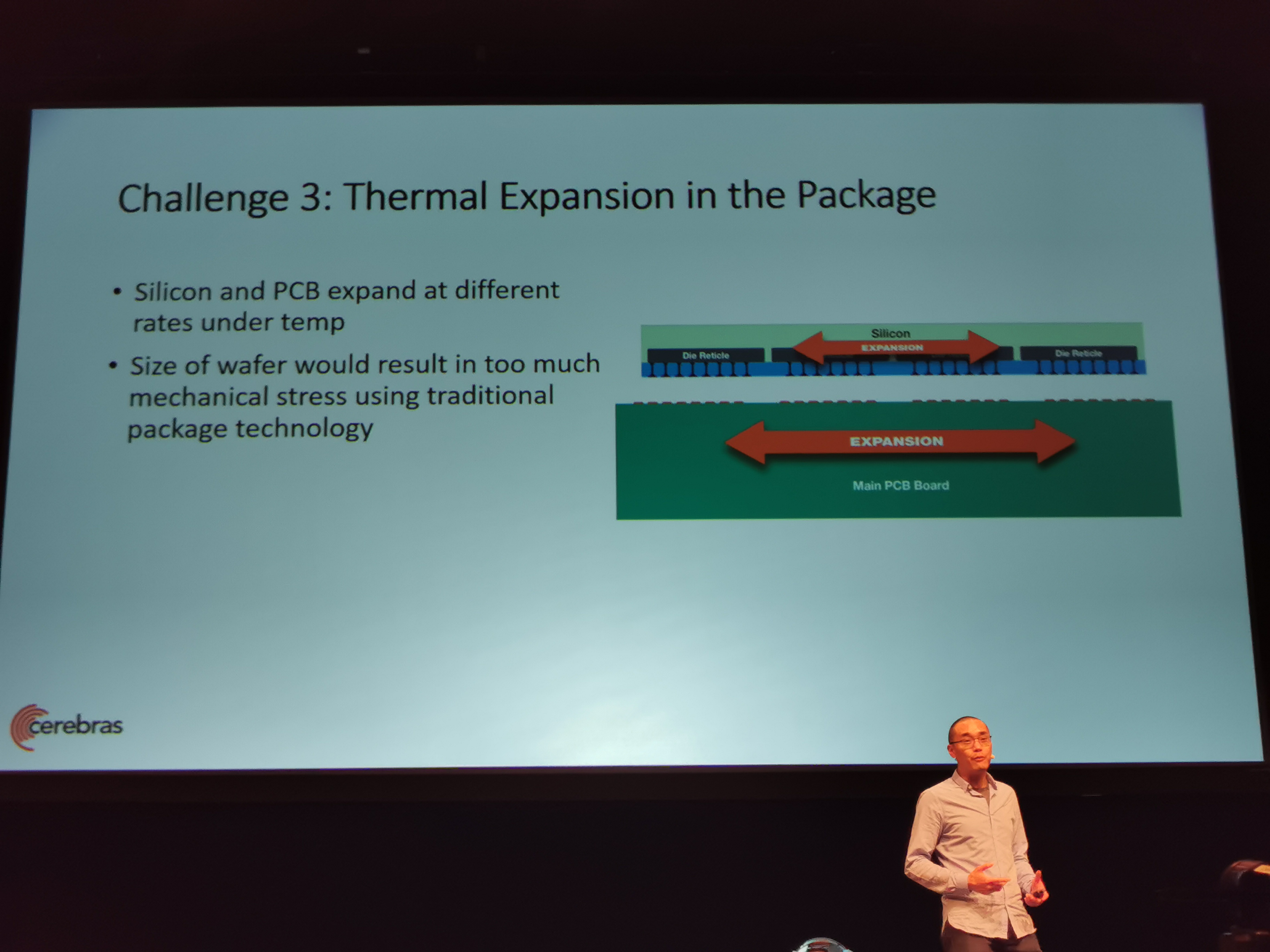
09:09PM EDT - Normal tech, too much mechanical stress via thermal expansion
09:09PM EDT - Custom connector developed
09:09PM EDT - Connector absorbs the variation in thermal expansion
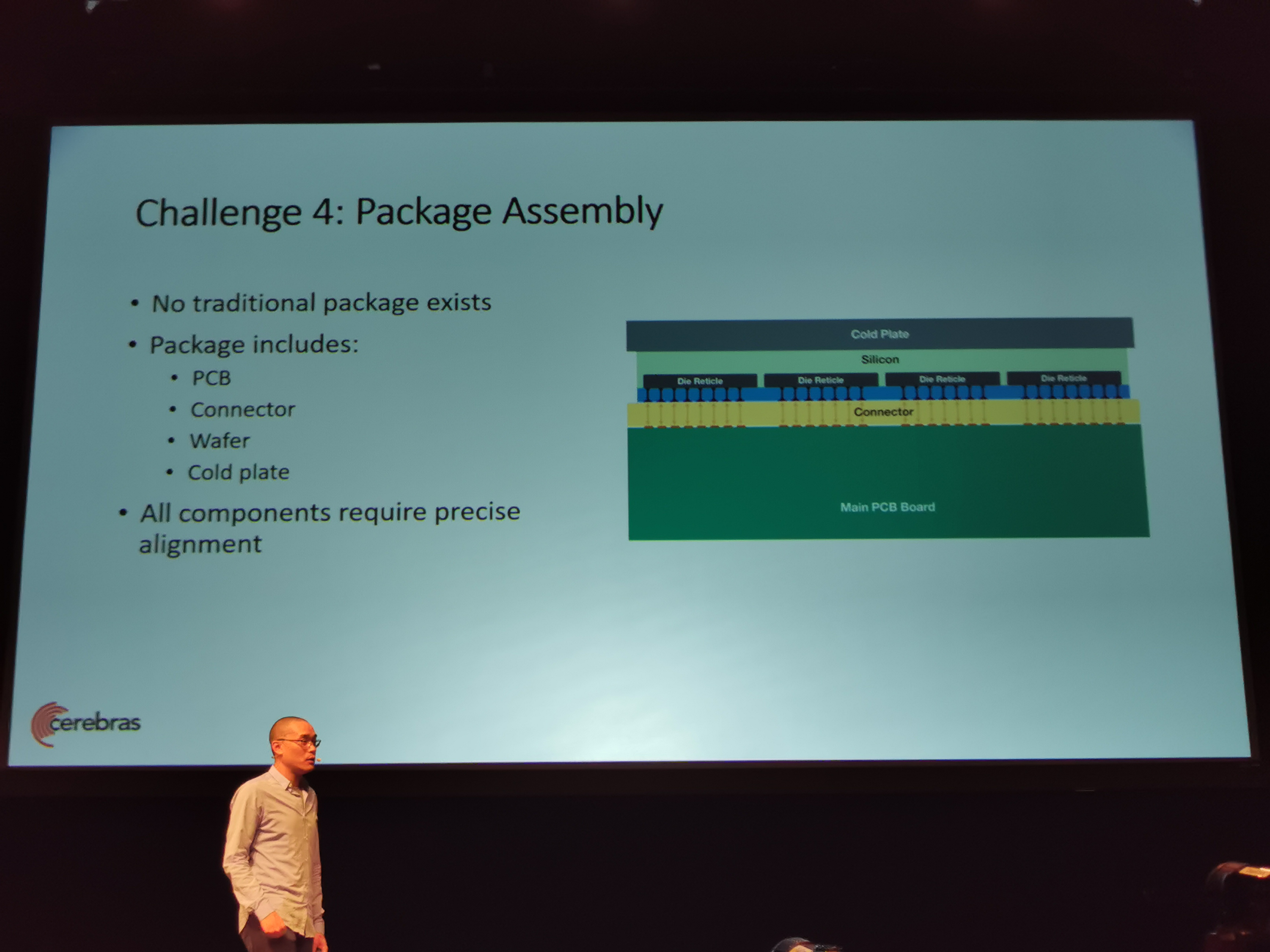
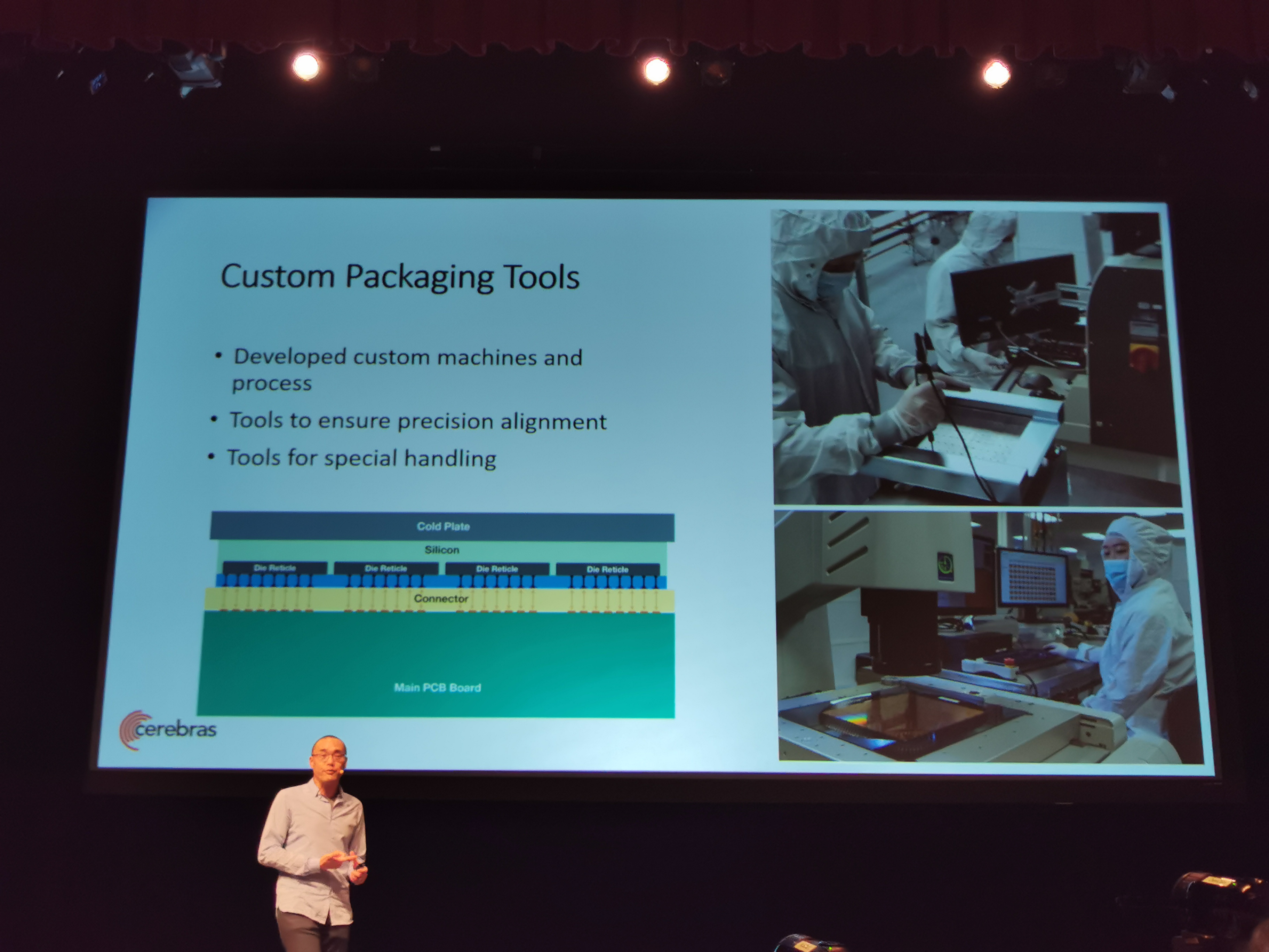
09:10PM EDT - All components need to be held with precise alignment - custom packaging tools
09:10PM EDT - Power and Cooling
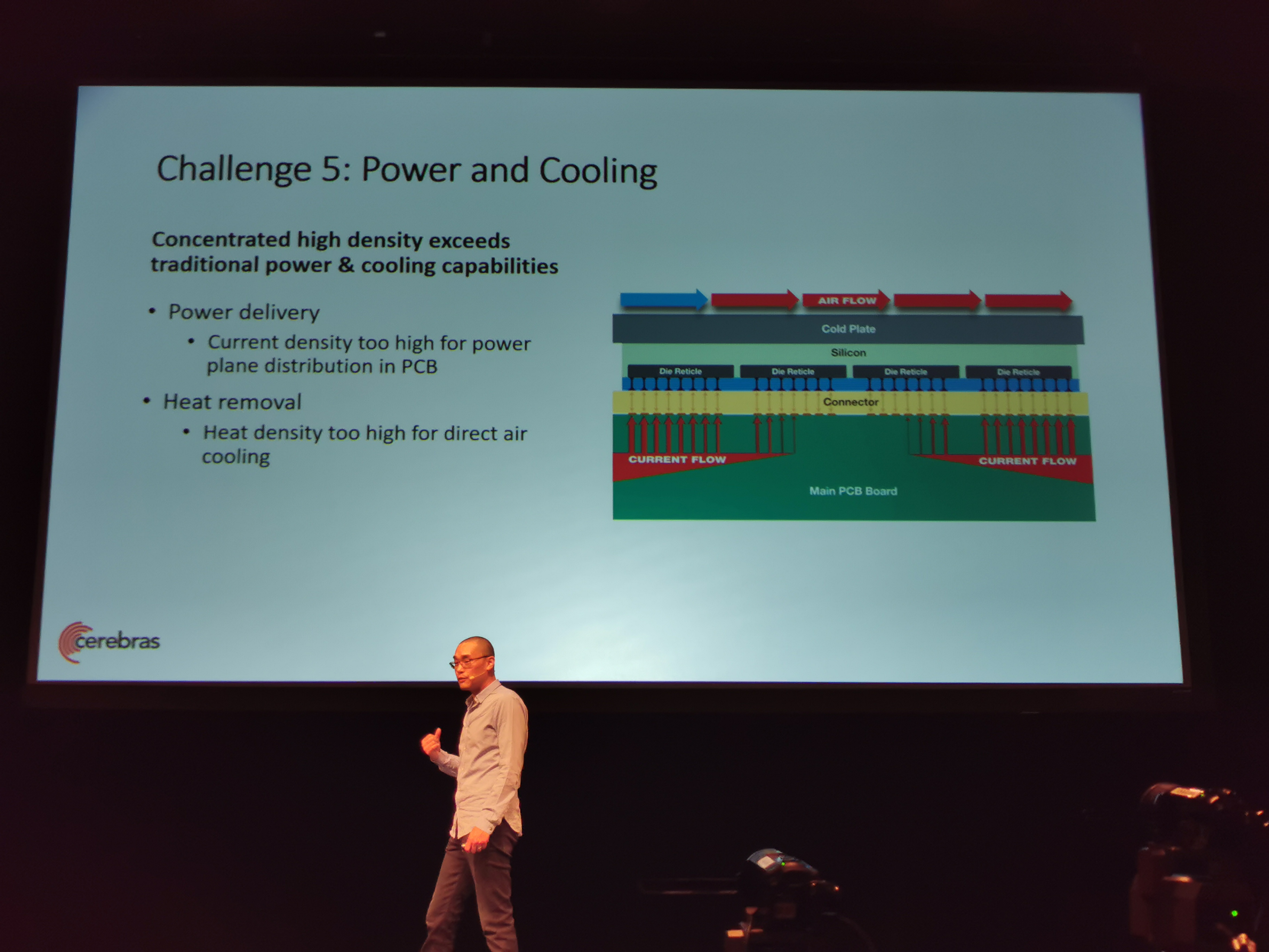
09:11PM EDT - Power planes don't work - isn't enough copper in the PCB to do it that way
09:11PM EDT - Heat density too high for direct air cooling
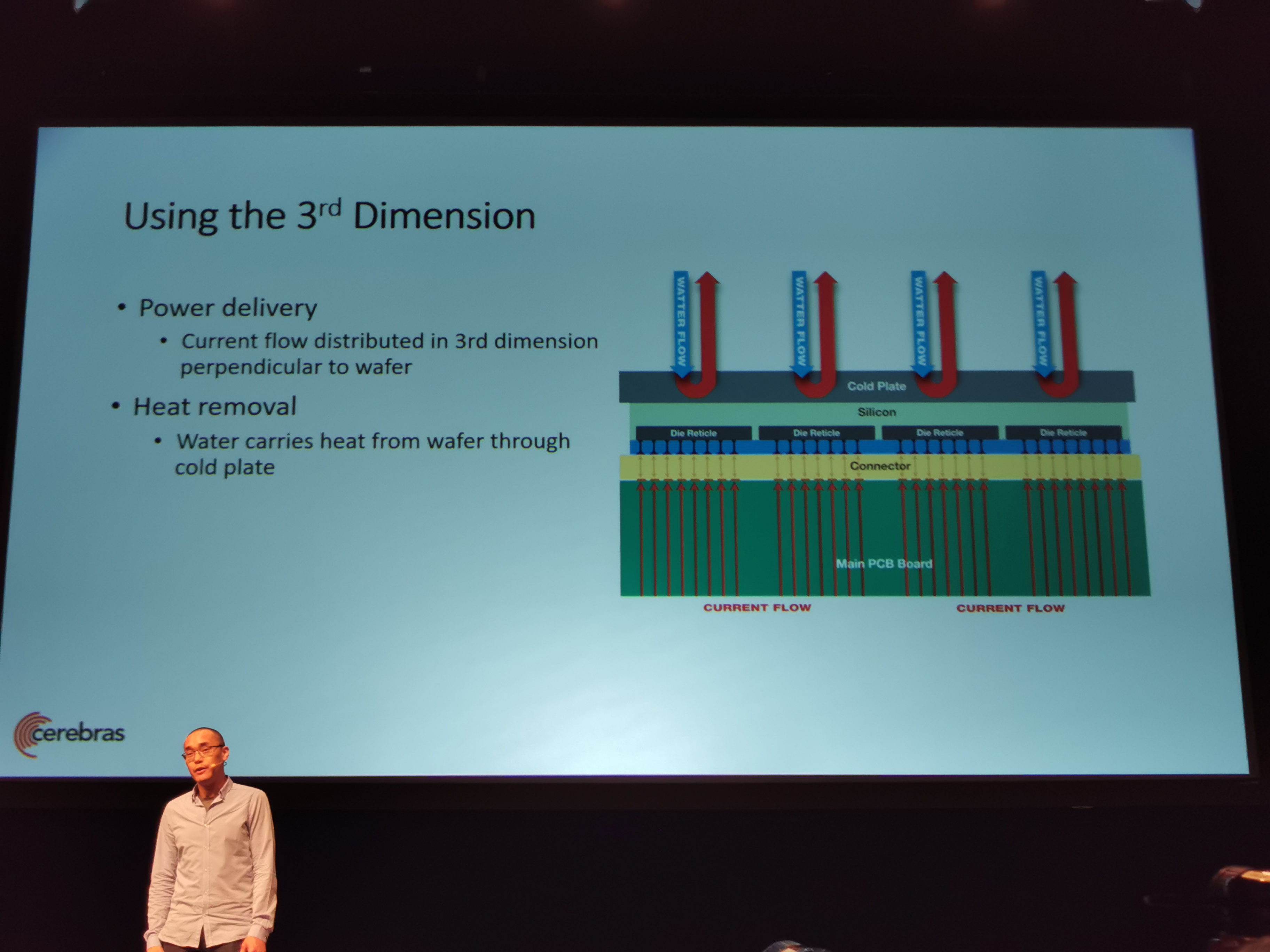
09:12PM EDT - Bring current perpendicular to the wafer. Water cooled perpendicular too
09:14PM EDT - Q&A Time
09:14PM EDT - Q and A
09:14PM EDT - Already in use? Yes
09:15PM EDT - Can you make a round chip? Square is more convenient
09:15PM EDT - Yield? Mature processes are quite good and uniform
09:16PM EDT - Does it cost less than a house? Everything is amortised across the wafer
09:17PM EDT - Regular processor for housekeeping? They can all do it
09:17PM EDT - Is it fully synchronous? No
09:20PM EDT - Clock rate? Not disclosed
09:20PM EDT - That's a wrap. Next is Habana


28 Comments
View All Comments
obama gaming - Thursday, August 22, 2019 - link
I asked a similar question on Quora regarding wafer yields, and an employee of Cerebras answered it thankfully. To quote him:Manufacturing an entire wafer without an error is impossible, but Cerebras found a way around it. The Cerebras WSE is made of 84 processing tiles, similar to individual chips, and each tile has redundant processor cores, memory, and I/O. When one part of a tile fails, the extra functions are substituted in their place through software tools, making it seem like a fully functioning tile. As a result, the company can theoretically have 100% yield of all tiles on a wafer and all wafers produced
drexnx - Tuesday, August 20, 2019 - link
"everything is amortized across the wafer"talk about a non-answer to the question - "depends on the house" is probably a more accurate one
Adam7288 - Tuesday, August 20, 2019 - link
More precisely, it depends on how many customers they have. If they have spent tens of millions on development and only have 10 customers, well they will be paying a lot more than if they have hundreds of customers.Santoval - Tuesday, August 20, 2019 - link
That's quite impressive, though I am not sure if they made this more as a proof of concept than as a viable product. By the way, despite mentioning that the *silicon* is 46,225 mm^2, which assuming the (monster of a) chip is a perfect square indeed corresponds to 21.5 cm x 21.5 cm, the numbers do not quite add up.A square with 21.5 cm sides has 30.40 (=>21.5 x √2) cm diagonals, which is larger than the size of a 300 mm wafer. Thus there is no way to make a square die with 215 mm sides and reach that die area unless you move up to a 450 mm wafer, which as of right now is on ice. My guess is that the entire chip, along with its package, is a square with 215 mm sides.
Clipping or rounding the corners of the die a little bit would also not result in these area and side numbers. Allowing a headroom of 0.5 cm for each corner to make the fab process more comfortable the die should have at best 20.5 cm sides for 29 cm diagonals and a die area of 42,025 mm^2.
peru3232 - Tuesday, August 20, 2019 - link
as I know they are not 300mm - it`s 12" ;)EETimes have more details - it seems to be not only a concept: "The whopping 46,225mm2 die consumes 15kW, packs 400,000 cores, and is running in a handful of systems with at least one unnamed customer"
really amazing!
And yes 450mm (18" hehe) is on ice, but maybe this is in future a turning point for the research...
eastcoast_pete - Wednesday, August 21, 2019 - link
15 kW? Doesn't that make their claim of being more efficient a bit relative? How many dedicated but smaller deep learning accelerators that already exist can one run on that kind of energy budget? I get the argument that the fastest solution is the one where the information being worked on basically never leaves the chip, but how does this really compare to more conventionally sized solutions?Duncan Macdonald - Tuesday, August 20, 2019 - link
The pictures above showing the cross die connectivity show that the device is NOT a perfect square. The device has an array of 7 by 12 dies each of which is rectangular not square.Santoval - Tuesday, August 20, 2019 - link
Yes, the small dies are rectangular and form a 7 x 12 pattern but the full die is still a square. Check out the "Cross-die Wires" picture which shows the full die overlaid on the wafer and you'll understand why. It wouldn't make sense to make the entire die rectangular, because they would have wasted even more die space from the wafer.Cutting a perfect square from a circle wastes less space than cutting any other rectangular shape from it (an octagon would have been much better, but let's not get greedy). In the last picture we see the real die, not a rendering, and it's clear (despite the perspective of the picture playing a little bit of trick) that it's a perfect square.
atearen - Tuesday, August 20, 2019 - link
1 chip per wafer and 18GB of SRAM, how much should they charge to make this financially viable?Duncan Macdonald - Tuesday, August 20, 2019 - link
Depends on how many they sell and how much the R & D cost was. The cost per wafer (around $5000) is probably a small part of the total cost. It will also depend on whether they can sell a cut down version to use up wafers with too many defects. (An individual die could be mounted on a PCIe card in a conventional computer - the full product requires a specially designed system.)