Intel’s EMIB Now Between Two High TDP Die: The New Stratix 10 GX 10M FPGA
by Dr. Ian Cutress on November 5, 2019 8:30 PM EST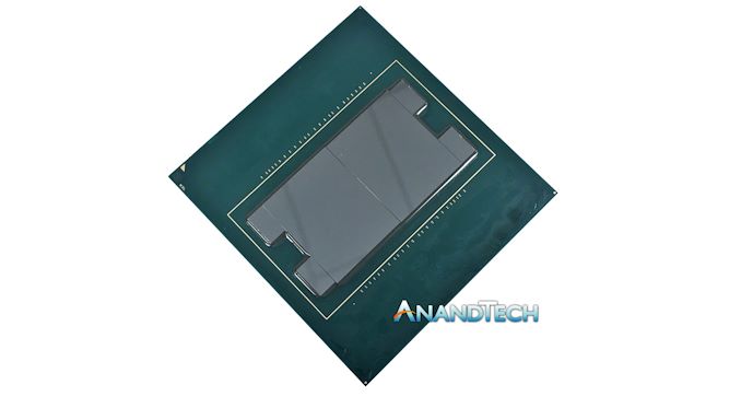
The best thing about manufacturing Field Programmable Gate Arrays (FPGAs) is that you can make the silicon very big. The nature of the repeatable unit design can absorb issues with a process technology, and as a result we often see FPGAs be the largest silicon dies that enter the market for a given manufacturing process. When you get to the limit of how big you can make a piece of silicon (known as the reticle limit), the only way to get bigger is to connect that silicon together. Today Intel is announcing its latest ‘large’ FPGA, and it comes with a pretty big milestone with its connectivity technology.
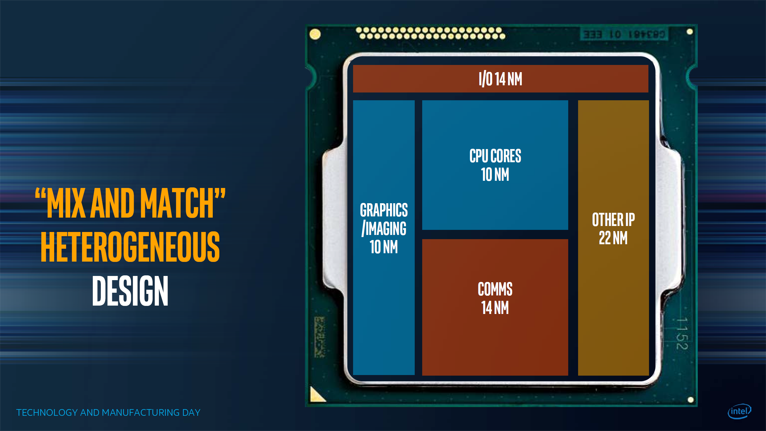
One of the elements driving this industry forward is packaging technology. We’ve covered in detail elements like TSMC’s 2.5D Chip-On-Wafer-On-Substrate (COWOS) packaging used in GPUs, Intel’s embedded multi-die interconnect bridge (EMIB), stacking technology like FOVEROS, and as we migrate into smaller chiplet based silicon, each will become crucial to finding the best way to produce the end chip that goes into a million systems.
Despite Intel’s best diagrams about its EMIB technology, showing many die connected together from multiple different process nodes, one major barrier has eluded the company. Until this point, all we had seen from EMIB was it connecting one high-powered die, like a GPU, to a low-powered die, like HBM. One of the criticisms to having only known Intel products connect one high-powered and one low-powered die is if the EMIB connection wasn’t thermally stable to withstand power-cycling between two die.
One of Intel's mock-ups of how future processors might look like
When connecting two die together in a substrate, especially high-powered die with vias or a BGA design, mechanical stresses have to be taken into account, especially if different metals are at play. Thermal expansion and contraction is a critical point of failure, especially when dealing with embedded and long life-cycle designs. Not only the expansion and contraction of metals, but when dealing with organic substrates holding the packaging technology, making the substrate inextricably thin also severely increases long-term feasibility concerns, especially if high-powered die are used for connectivity.
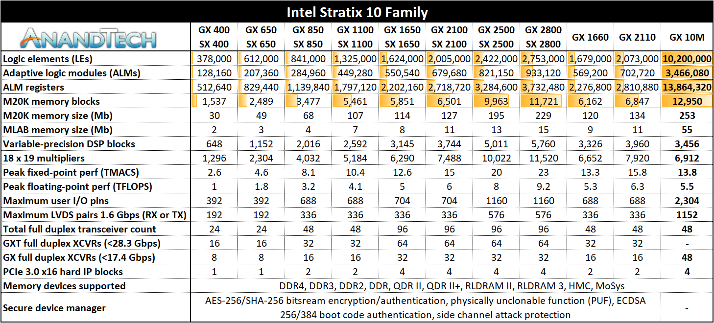
With Intel’s new FPGA, the Stratix 10 GX 10M, the concern seems to have disappeared. This new product, designed as a big FPGA for the ASIC prototyping and emulation market, combines two large 5.1M logic element FPGAs with three EMIB connections, producing an overall chip with an average TDP from 150W up to 400W with advanced cooling.
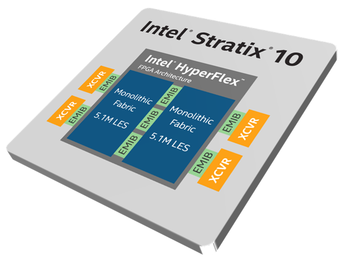
A total of 7 EMIB connections, but it's the three in the middle that are the milestone
The ASIC prototyping and emulation market, while a small market revenue wise (Intel stated ~$300-$500M/yr), is always requesting bigger and bigger FPGAs in order to be able to fit more and more of their ASIC designs onto as few FPGAs as possible in order to get the most accurate results. These chips ultimately end up running at a low frequency for accuracy, anywhere from 50 MHz to 300 MHz, but Intel states that this new Stratix 10 GX 10M design can easily replace four of its old GX 2800 FPGAs with double the connectivity and even a 40% power reduction for the same workload.
The design of the FPGA is around those two 5.1M logic element dies, connected together with three EMIB connections. These use the AIB protocol running at over 1 GHz, and form part of the 25920 connection pins across the whole chip which has another four EMIB connections to transceivers as shown in the diagram.
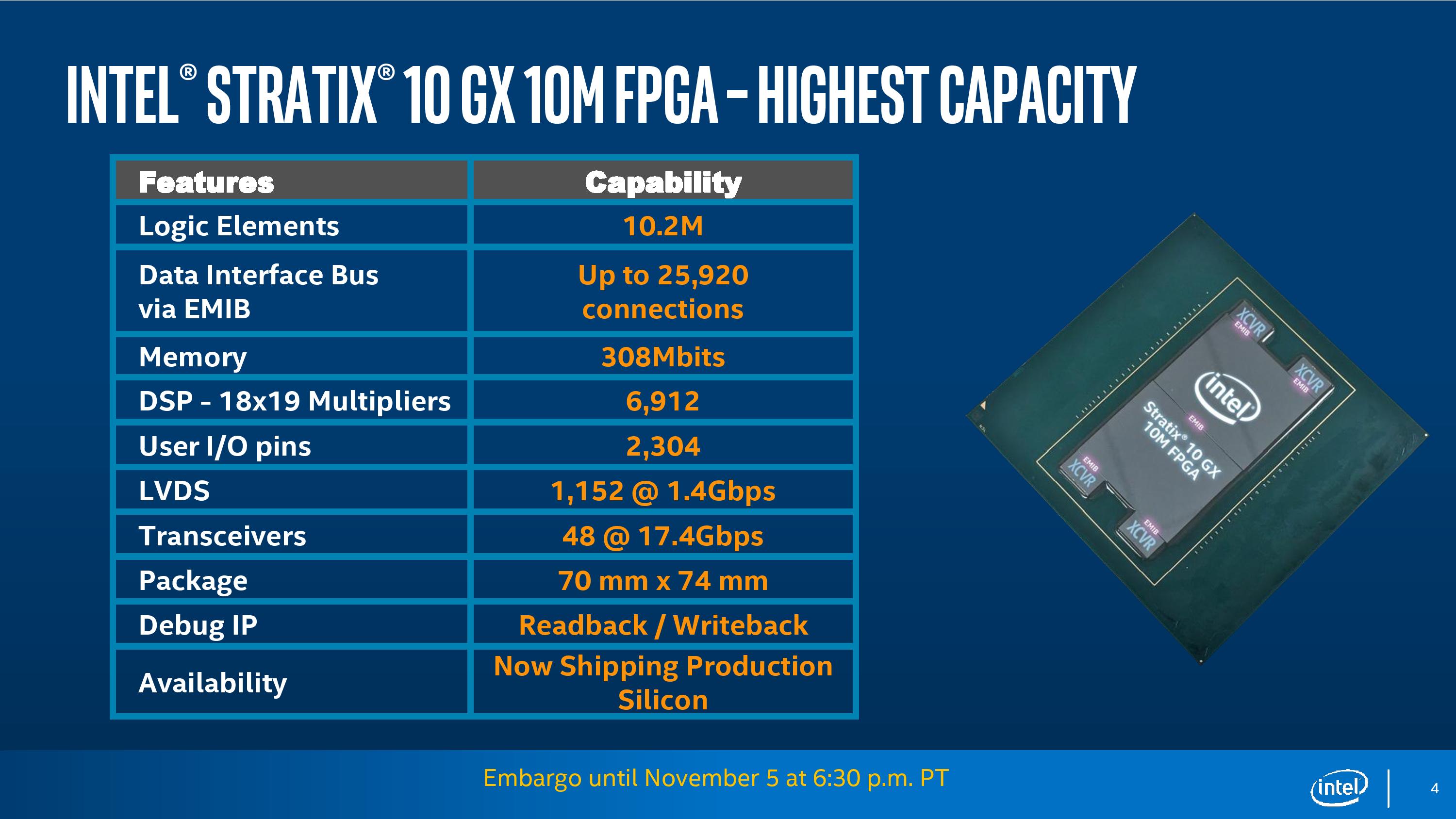
At 10.2 million logic elements, this FPGA eclipses the Xilinx VU19P announced in August which had 9 million elements (8172k flip-flops, 4086k LUTs). The Stratix 10 GX 10M also contains 6912 DSP elements and 48 transceiver outputs at 17.4 Gbps. Intel states that these are designed primarily as PCIe 3.0/4.0 support, and that the FPGA supports H-tiles for connectivity for customers interested in custom designs.
The launch of this new hardware coincides with Intel’s FPGA Tech Event in China, which is one of the primary markets for this product. Intel states the hardware has already been with key partners almost a year (one of the early customers is China based), but is now in production for the wider market. On the topic of Intel’s high demands for its 14nm parts, the company stated that the volume isn’t that high for this sort of product, and they won’t have any issues. The company (at least, the FPGA part of the company) did explain that the use of EMIB in this fashion means that their two-die approach assists with yield.
Personally, the fact that Intel is strapping two high powered die (~75W to ~150W each) together using multiple EMIB connections is a key step into driving the EMIB technology to the wider market. With this as a proof of concept, it paves the way for better multi-die CPU designs as well as the promise of EMIB (and Foveros) in future discrete GPU products.
Related Reading
- Xilinx Announces World Largest FPGA: Virtex Ultrascale+ VU19P with 9m Cells
- Intel Acquires Omnitek: FPGA Video Acceleration and Inferencing
- Intel Announces The FPGA PAC N3000 for 5G Networks
- Intel To Acquire eASIC: Lower Cost ASICs in FPGA Design Time
- Xilinx Announces Project Everest: The 7nm FPGA SoC Hybrid
- Hot Chips: Intel EMIB and 14nm Stratix 10 FPGA Live Blog
- Intel to Acquire FPGA-Specialist Altera for $16.7 Billion
Source: Intel


31 Comments
View All Comments
Guspaz - Thursday, November 7, 2019 - link
Just a reminder that FPGAs are also becoming increasingly prevalent (in visible roles) in the consumer market. Many popular scaler and HDMI mods for classic game consoles are FPGA-based, and while those may be niche, products like those from Analogue are built in far larger quantities. Unfortunately, cost is still a big barrier: Analogue’s consoles are stuck at 140k LE for cost reasons, and while the mister features several times as many, it’s only viable for consumer use because the project is based around a subsidized development board.All that to say it would be interesting to see coverage of FPGAs on the consumer electronics end of the spectrum, rather than simply the enterprise end.