An Interconnected Interview with Intel’s Ramune Nagisetty: A Future with Foveros
by Dr. Ian Cutress on January 3, 2020 9:00 AM EST
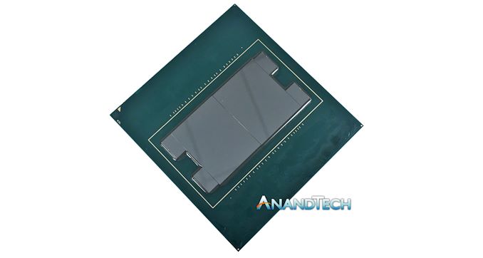
I’ve constantly stated for the last two years that the next battleground in performance for the semiconductor market is going to be in the interconnect – whether we’re speaking about on chip with new manufacturing technologies or new topologies, or between chips with new communication standards or connectivity paradigms that shake up both bandwidth and efficiency. Moving from monolithic designs to chiplets and stacked silicon requires a fundamental shift in thinking that most of the industry is not yet ready for, from silicon engineers to vendors who design the software that enables silicon engineers to do their thing. You might not be surprised that Intel has a whole department dedicated to these new interconnect and packaging technologies. Ramune Nagisetty works across Intel's broad range of process and packaging technologies as Director of Process and Product Integration, and I finally got a chance to meet Ramune at this year’s IEDM conference. We sat down for an interview to discuss the area.

IEDM is fun for everyone
Joining us for our discussion is David Schor from Wikichip.
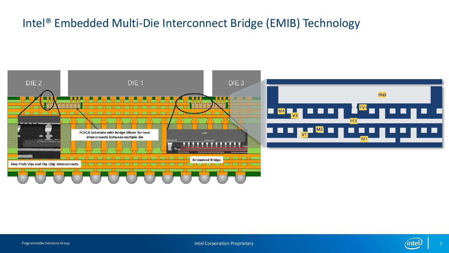
One thing to get right is standards, allowing multiple companies to work together in a mix and match scenario. Ramune is a big fan of bringing multiple companies together, particularly memory companies with logic companies, to ensure that these standards work together but also result in co-optimized chips and products to drive the industry forward. The key part in this is introducing people to the concept, but also looking at the three-to-five-plus year roadmap about where this is going. Chiplets and connecting chiplets isn’t a new concept, but Ramune is at the forefront of Intel’s design capabilities on how those chiplets are connected, either horizontally though package connections or EMIB, or vertically stacked as with Foveros.
You can follow Ramune on Twitter.
As always with our interviews, the transcription has been tidied up for readability and the questions may be rearranged to keep certain topics together.
Roadmaps for EMIB and Foveros
Dr. Ian Cutress: One of your engineers this week mentioned a second generation of the 3D stacking Foveros technology. What does Intel’s roadmap look like for this technology?
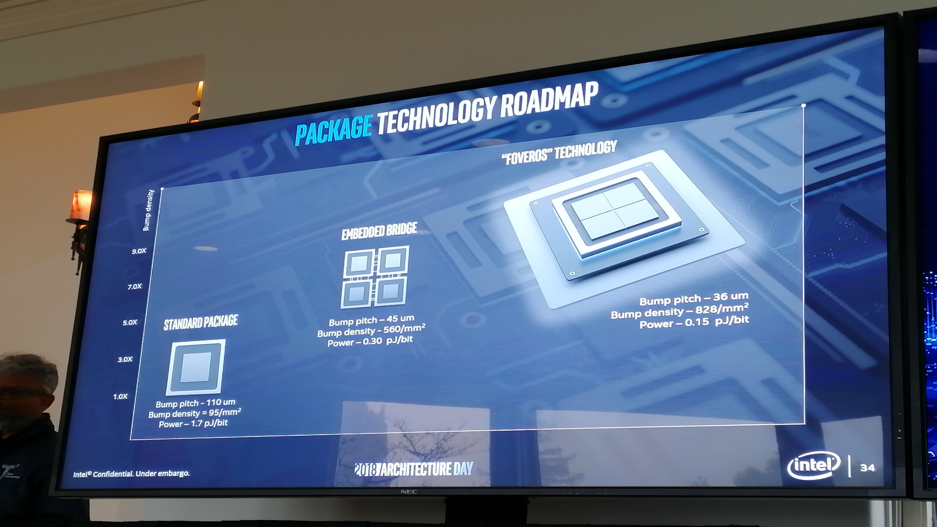
Ramune Nagisetty: Every single one of our packaging technologies has a roadmap, and it’s all to do with scaling. None of our interconnect plays are one-trick ponies – they’re going to scale into the future. The main feature with some of these technologies is the pitch scaling – the microbump scaling as you move from die-to-die and the TSV (through-silicon via) scaling as dies are stacked. We should at some point show or disclose the roadmap for these just to show where we are on the path for it. The cadence for each technology might be differentthen a normal product roadmap cadence, so that is something to consider.
Having a roadmap is a good thing – I wouldn’t want to be landing our products on a packaging roadmap that didn’t have a vision for scaling into the future. I mean we’ve seen 55 micron, into 45 micron, and then ultimately hybrid bonding with 10 micron bump pitches is on the horizon as well, but these things are in the future – they’re essentially ‘pre-roadmap’ technologies still in the research phase. The real skill is in determining when to take one of these technologies from the research phase and put it into pathfinding and development. The critical aspect here is timing, and so today I talked about how we patented EMIB over a decade ago in 2008, and started writing papers on it in 2011. It only started shipping in 2018. So when you decide to use these technologies, not only how you use them, is really the skill that’s involved.
IC: Would there ever be a time when some of these new packaging technologies actually drive at a scale that makes them cost effective for price sensitive markets?
RN: I think so. I think this is the beginning of the way we will be creating products in the future. It’s not to say that we won’t have some products that are monolithic SoCs, but in the future it will be a healthy mix. Where I spend my time is working on technologies in that three-to-five year horizon, and actually stretching beyond that, so I think that these technologies are going to fundamentally change the way we actually plan our roadmaps in the future. I think that five years from now, when we look at how we do a product roadmap, it may actually be based on the packaging technology and from the different templates that are available, and then we put the products together. So it will be probably quite different than the way things are today, which is where everything is locked together in a monolithic SoC. But once you unlock those things, the way that you put products together will change. We are at that cusp.
An Industry Ecosystem
IC: Intel’s driving a lot in its own ecosystem, and AMD has being going down the interposer and chiplet approach. Is there a point in time where we should be saying ‘hey, let’s all do this together?’
RN: What I really am championing is the concept of an industry scale ecosystem where we can have a mix and match of chiplets and intellectual property that are produced at different foundries and different companies all coming together. Actually I think that this is going to unlock a bunch of innovation in the ecosystem that today is stifled because of the really high cost to entry. Even in terms of designing a full monolithic SoC, the design aspect is formidable and then manufacturing is even more formidable. If we build a mix and match ecosystem, it allows the smaller players and even universities or startups to be able to get in on this.
I think that when you develop these clearly defined interfaces and contracts, like the conceptual term of a contract between one chip and another, it will allow the ecosystem to flourish outside of those previously fixed boundaries. We’ve see a lot of that happen partially today, where we have soft IP and hard IP that’s provided to foundries, and I think that this will happen in the world of chiplets as well – at least some extension of that. We’ve started doing a lot of work, and I’m sure you’re familiar with the DARPA Chips programme. For example, there is a startup called Ayar Labs which is developing a chiplet for silicon photonics. Universities are developing chiplets for machine learning acceleration. So all of this, what we’re doing with interconnects and packaging technology, puts this in reach of startups and universities. It will offer another dimension of innovation that is basically locked up today.
David Schor: The Open Compute Project started a new working group earlier this year called the ODSA, striving for a chiplet ecosystem. One of the things they talked about was how much of a challenge this is logistics wise – how do we know how much of our IP to share, how much control is given to each side of the connection, and how do we maintain consistency across designs. There’s a lot of discussion about inter-chiplet communication and control.
RN: I know the ODSA, and I’ve been to a few of their meetings. There are a lot of issues that have to be resolved before this type of ecosystem can flourish. I think one of them is actually having access to the advanced packaging technology. It’s very well to discuss control and things before having the ability to manufacture it, but when you can do that then it gets easier to define the interfaces.
As you know, ODSA is working on a technique called ‘Bunch of Wires’, or BoW. (IC, sarcastically: that sounds very technical!). As it stands, the approaches that ODSA are taking are not really based on advanced packaging technology, primarily because it’s not widely available to them, and so the interfaces they’re working towards have to also be supported with standard packaging technologies and organic substrates.
DS: Does Foveros have a standard interface so other companies can use their chiplets?
RN: Not yet. It would have to be co-designed with Intel. Even in the beginning of this future that I envision, there will be collaborations with memory companies to figure out how to create a standardised product because they don’t want to be creating custom products for everyone as that’s not cost effective. For us, I think there will be some sort of industry collaboration to figure out how to get some sort of standard memory interface definition.
DS: What do you think about this new ITRS-like heterogeneous roadmap document that’s being compiled?
RN: I’ve read the first chapter, and it’s a pretty good! I mean they have a chapter on medical devices, and other chapters on things that I don’t get involved with. But I think it’s good that people are working on this and predicting where the future is going to be headed – we have Intel people that have contributed to the document. It’s good to recognise the industry is headed this way and that helps things where there’s industry-wide recognition that this is a path to go down – in the same way that the ITRS roadmap helped align the industry.
Implementation and Thermals
IC: That’s the other argument with these packaging technologies, in that are the communication protocols in place ready for intra-chip and inter-chip communications. Intel has a unique position in that it can define all of those right now, and as Intel has disclosed with its new Ponte Vecchio design, we have this sort of multi-layered product with Foveros, EMIB, and it looks like some interposers on there as well.
RN: This is still the kind of tipping point for interfaces. We’ve already demonstrated our AIB interface in products today (the Stratix 10 GX 10M) which uses EMIB and logic chip to logic chip integration. But HBM as an interface was essentially the first proof point of an industry standard interface, and with AIB we have a second proof point as well. There’s a tension that the market could go towards proprietary interfaces that could be higher performance, but are not backwards compatible. You might see that with some tight product design co-optimization, but we need industry standards in place for everyone to get in on the ground floor.
At Semicon West we gave some details about the second generation of AIB, and there’s a future roadmap there for improving the interface in terms of overall power efficiency, but just like anything where you decide that you want to make it a standard, it has to have some backwards compatibility otherwise it doesn’t help as much as it hinders. You have to have some kind of decision point as to when we are going to be releasing the most efficient interfaces into the ecosystem but lose some backwards compatibility, or are we going to back up our approach and be very firm about interfaces that are open but also backwards compatible. This comes at a cost versus always moving towards the leading edge, and then falling behind in terms of the concept of supporting interoperability – our approach does take some discipline. Is interoperability going to be the stake we want to put in the ground? This is a question we ask ourselves.
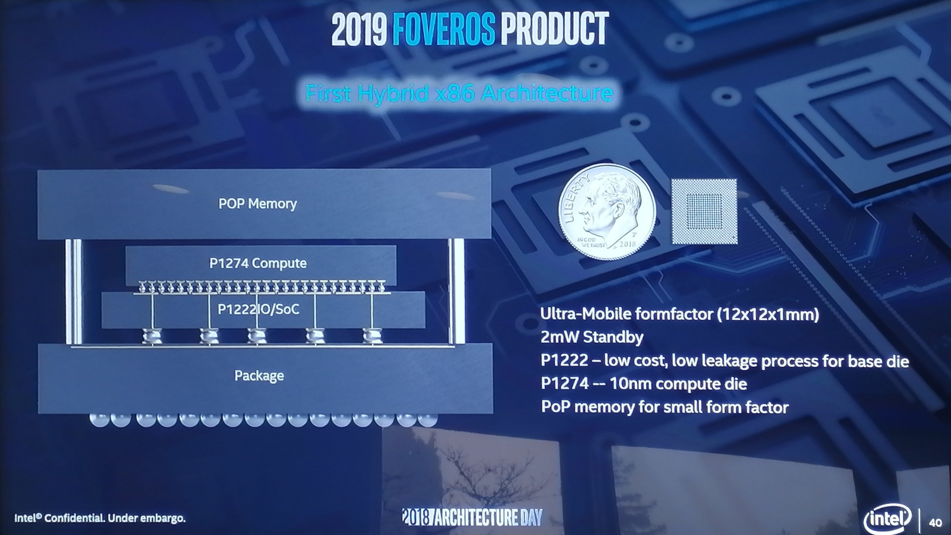
IC: Do you find that the people who want to implement these packaging technologies either want the best performance, or the best power efficiency? Take for example Intel’s current Lakefield product is all about power efficiency for 3D stacking, providing a sufficiently low amount of power in that small of an interface, or the other extreme is the FPGA using EMIB to get the highest performance between two FPGA die. At the minute I feel like we’re seeing two opposite ends of a spectrum.
RN: One thing to realise is that vertical stacking and horizontal integration solve two different problems. When you have vertical stacking you have to be very power efficient because you otherwise end up with thermal constraints that will limit the performance of the system. But it’s a good point – we’ve spoken about 2.5D integration, then 3D with Foveros, and Intel has also disclosed the ODI, the omni-directional interconnect. It’s been talked about here at IEDM as one of the most interesting interconnect technologies as it allows you the opportunity to have a bigger die on top of a smaller die, or you can have cantilevered/shingled die together kind of like NAND flash and this technique can give you better connectivity. You have to design with these things in mind, and with something like ODI it can give you much better connectivity while also balancing the thermal constraints by covering or not completely covering the bottom die with the top die. Overall I think that different integration schemes work together, but thermal issues arising from die stacking is a strong area to work at.
IC: Can you talk about how you are addressing the thermal issues?
RN: Part of it is co-design. One of the things that is a factor in terms of a future industry scaled ecosystem with interoperable chiplets is going to be thermals, and the way that thermals often are addressed with die stacking is that these die need to be planned together, to cope with both power requirements and thermals. The kind of co-design of those chiplets typically means that, in the first generation of interoperable chiplets, there are not going to be many layers because the co-design between top, middle, and bottom die are so critical. With 2.5D designs, the interoperability is more clear and easier to handle. So in the future I do think interoperability will make its way into 3D stacking, and what I expect to see a lot of is memory stacking.
Today, memory is a very specialised technology that comes from specific companies. In order to maintain their business model, they have to drive standards. Everyone else has to adhere to these standards, because everyone needs memory. So 3D memory stacking with logic is in on the horizon, and at Intel we’ll drive interoperability in that 3D space as well. So for example, we could see 3D stacked designs with alternate layers being memory, using a general template for the physical design and the mechanical interface. If the templates are designed from that perspective, then we hope it should all work together, thermals permitting (and that’s where the co-design comes in).
Foveros For The Future
IC: One of the issues with 3D stacking, especially as you go beyond two stacks which is where Intel’s future lies, is getting enough combined dies to yield appropriately. Can you talk about the redundancy that’s built into Intel’s stacking technologies, and how this helps?
RN: So we do have redundancy built in. We do a lot of really heavy use of DFX, which stands for ‘Design for X’, which could be designing for test, or design for yield, and we scan at each stage. There is also singulated die test technology that we can do before stacking the dies to ensure that we’re putting two guaranteed known good die together before they become a package. So between the kind of design for yield/design for test and advanced testing capabilities, this is how we will move forward in terms of guaranteeing known good die. You are right, it’s an important factor to discuss, especially not only because it’s the yield of the die but also the yield of the process of combining those die.
DS: Do you see that direction, going beyond two to three to four stacked die?
RN: Oh yeah, definitely.I think you might have seen one of the slides presented the other day where there are all sorts of different logic technologies that are possible for integration, like power delivery technologies based on gallium nitride and such. So if you look at that you can already see that there’s power delivery, there’s memory, there’s IO, and there’s logic. So with the logic, that could also be split up into leading nodes and older nodes as well, within the same package.
IC: Has Intel discussed about integrating its 3D XPoint into these connecting technologies?
RN: I don’t think that it really fits well in the memory hierarchy space for it to be an in-package memory. There’s space there for the last-level-cache type of memory, but I don’t see 3D XPoint moving into that space.
IC: One of the issues that needs to be addressed due to stacked packaging technologies, now that we’re looking at something other than a monolithic design, is the variable z-height with the products and what that means for actual end-product integration. How often do those z-height conversations come into play?
RN: A lot. These layers when manufactured need to be thinned, or sometimes a dummy die has to be added in order to ensure that the end thermal solution requires all of the die on the package to be at the same height, so there can be some shimming or dummy die that are placed in there. These dummy die are not patterned, they’re not active, and they’re there just to basically help with the thermals. It’s definitely an issue and it’s a really important point because it is often just an afterthought to some of these discussions. People turn round at the end of production and get to assembly with their thermal solution and the feedback is that this could have been thought of in advance, especially when you’re taking silicon from different companies and stacking them together – and you know not everyone has the same die thinning capabilities as each other as well. So part of the mechanical standard we want to drive also includes that z-height aspect.
IC: Should we ever expect Intel to state in a stacked design if a dummy die was used? I mean, we’ve been told that Lakefield has two die stacked together but there could be more inside?
RN: You know I don’t even think it would occur to the product team to even say anything about it. I mean, it would be obvious if you got the chip and had the facilities to do a tear down. I think that people probably don’t talk about that because it doesn’t sound as if it’s on the leading edge, it’s not the most exciting thing in the world. Often at times dealing with thermal solutions isn’t the most exciting thing in the world that people want to focus on.
DS: With the current Lakefield product, the memory on top is a PIP type of design, and because the memory and the logic die are not directly connected, the data has to go down through the big pillars and back up the die stack in order to reach the cores – it’s doing a big loop, despite the memory being right there next to the logic die. Was that discussed in the design?
RN: It’s as I said before, because of these memory vendors we want to get them all working together on a standardized mechanical and protocol interface such that the DRAM can become part of the 3D stack in its own right, and then we can bypass the method that’s already been deployed. What you’re suggesting isn’t going to happen over the coming weeks or in 2020, but it’s definitely near the tops of our lists that we need these interfaces. We just have to have the right collaborations going forward for in-package stacked memory.
DS: Not only memory, but I could also talk about other things mentioned at this conference being on that stack.
IC: Like 4G/5G modems? [laughs]
RN: [laughs] No comment!
IC: The current 3D stacked announced parts, namely Lakefield, is on the order of under 100mm2. Does that mean that there’s ultimately a limit to how aggressive Intel might want to be on the die size for each of the stacked layers? It’s likely to affect yield and other things – would higher stacked but smaller die win out over large die of a few layers?
RN: With the die thinning and thermal issues, there are also planarity issues – the devil is in the details, especially when you put lots of extremely small die in a package, but there are also mechanical stability concerns between the packaging and the silicon interfaces. I think that there’s another area to consider, and that’s the aspect ratio of the die, like if you have really long tiny rectangular layers or more square die. These things have to be planned in advance as well in terms of die that don’t cause planarity issues or warpage issues because those that have those issues will translate into thermal issues and you end up with poor contact as well. Today we don’t really have any specifications for what the die size has to be, either as a minimum or a maximum, but if we want to create an interoperable chiplet ecosystem, these things will have to be specified so that not every solution is a custom solution.
Monolithic 3D and EDA Tools
DS: A few of the papers and discussions at the conference this week has been about ‘Monolithic 3D’, or ‘Sequential stacking’ (building two or more layers of logic in one piece of silicon). Do you see that coming to fruition, even on the decade time scale?
RN: Monolithic 3D is in the long term roadmap, I mean you saw what we presented in our plenary discussion about driving these sorts of technologies. The technologies listed in our presentation will drive 10 or more years of scaling. Along those lines, people say that companies rarely have insight or visibility into the future beyond 10 years, but in order to implement these technologies that’s what you have to look at.
When it comes specifically to monolithic 3D, it’s entirely possible to do it. The question is going to be of thermal issues as well, so I think you know the key issue when you’re doing die stacking is that we needed to think about our architecture in terms of optimizing for the power efficient corner of where we needed to be, and we’ll gain performance on top of that from adding additional transistors, functionality, and capability with each layer. With a monolithic 3D design, we might not be able to reap that benefit if we continue with a design approach that is focusing on the optimization for the performance end of things.
So there’s a really important mind-set shift that the performance of the whole product might be better if we actually target the more power efficient core on the silicon, because with die stacking you get a lot of performance from these other aspects of integration that weren’t available in the past.
So from a design and architecture point of view, there needs to be a real rethinking of how or what performance means and how we get it. You must be really familiar with this when people, you know even within Intel, are targeting performance often at times just for the performance of their individual silicon block instead of the performance of the integrated product as a whole. That’s the mind-set shift that needs to take place to take advantage of these technologies.
One of the main things that we have to consider is that with something like tightly-coupled 3D stacking is that the whole EDA ecosystem has to be able to handle these needs and these types of designs. Software even for chiplet stacking still needs to evolve – and monolithic 3D tools need to evolve too. Whenever there is new technology that looks really attractive, it’s imperative that the EDA ecosystem catches up to that. We’re working closely to make sure that at least we’re communicating with the EDA vendors what the future directions we are going to so that some of this development can happen in parallel and that we don’t end up with manufacturing technology ahead of what the EDA tools can provide.
IC: With Intel working on its own technology and in its own fabs, having those internal tools are great, but in order to drive a chiplet ecosystem beyond Intel, even to the memory vendors, it requires Intel to reach out to the EDA vendors to actually share this knowledge. That co-development is ‘free’, right?
RN: We’re doing that today, and we’re seeing a big change to the internal mentality to share what we need to share to drive this ecosystem. The EDA vendors have to have the tools ready so that we can actually utilize the technologies we’ve developed, but once an EDA vendor is enabled, they could offer it as a feature for everyone. There is a sensitivity around it because you’re basically disclosing what your near term direction is. But as you can see, there are a variety of directions to go in, so it’s important for us to be able to communicate with these tool vendors in advance. There are always NDA agreements in place, for example if we need a vendor to develop a feature but we don’t want them disclosing the details or capabilities just yet. But these tool vendors have to be involved – they work with many different customers, so there are ways that they handle this. I think they also understand that if they develop a certain capability for Intel, it might be only be useful for Intel initially in the near term, but there are always skills that are learned from developing this functionality. With stacking and interconnects, one way or another these capabilities will be needed.
IC: How much do you personally get involved with that, give you work at that three-to-five-plus time scale out from today?
RN: I interact with Synopsys, that’s the main vendor I interact with, even if it’s not on a frequent basis. I do get involved, maybe not at the very detailed level, but certainly at a high directional level.
Is the Future of EMIB on Desktop?
DS: Earlier this year Intel disclosed that it shipped its 2 millionth EMIB product. Do you see EMIB making its way into the mainstream desktop market, where you’re shipping 10+ million products, rather than just the high-end low volume hardware?
RN: Yes absolutely. Actually that’s the advantage of EMIB compared to some of these other integration schemes – the cost is in the volume, and that makes it manageable. That’s the kind of volume we want in order to amortize these costs.
IC: One of the worries I saw about EMIB was that Intel had never paired two high powered die together – only one high powered die and HBM – until we saw the latest Stratix 10 product line that does use two high-powered FPGA connected by 3 EMIB connections. Has that come about with generational improvements to the EMIB design?
RN: It really has to do with designing the chiplets. When you take board level components and put them together with EMIB, these parts weren’t designed to be co-packaged together, so you end up with concerns like you had, around thermal and mechanical stresses. I think this has to do with the mind-set shift I’ve been talking about – how we create our products boils down to how we think these chiplets are going to interact with each other, and they have to be architected from the ground up to do so. Not only that, but in the future they’ll have to play well with others.
This requires a broader view of how we create our products and how we benchmark the performance of individual components. We also have to motivate the teams that are working on these products – how do we set their priorities, and what goals are they working towards? So it really does waterfall all the way down to the architecture or microarchitectural level of the goals of these chiplets. So in some ways it can get more complex, but in other ways if we can define these interfaces and set goals for these individual pieces, then this is basically how we move forward.
Many thanks to Ramune and her team for their time.


19 Comments
View All Comments
JayNor - Saturday, May 22, 2021 - link
With Ponte Vecchio now described as a 47 tile emib and foveros GPU, the "long term" has just gotten shorter.HStewart - Friday, January 3, 2020 - link
I am curious what happening to original EMiB like Intel Chip in Dell XPS with AMD derived GPU. I assume that was really just plans to test ability of EMiB to use another companies GPU and likely Intel will use Xe in the future.chophshiy - Friday, January 3, 2020 - link
With all of the talk of thermal considerations at this level of integration, I'm surprised that microchannel cooling did not come up. I'm curious as to if Ian or anyone else there has had that discussion with similarly positioned design/fabrication folks.mode_13h - Tuesday, January 7, 2020 - link
I'd just like to know if she's named after the beverage:https://en.wikipedia.org/wiki/Ramune
officesetup - Tuesday, January 21, 2020 - link
Thanks for sharing this great post. It is very helpful for everyone.To know Office setup https://getinfos.org/office-setup/
johnronald2 - Thursday, January 23, 2020 - link
i like it <a href="google.com">very</a> much.ColtBergamo - Thursday, September 24, 2020 - link
I just cannot find enough words to express my gratitude. https://termpaperwriter.org service met all the requirements and finished my essay before the deadline without any mistakes or typos or in general any drawbacks. But for you I might have been expelled since my professors were really dissatisfied with my previous papers.pirspamela90 - Tuesday, December 15, 2020 - link
It was interesting to read this presentation and to know more about new Intel. Follow https://sportpeptides.com/ to read my site.JayNor - Saturday, May 22, 2021 - link
Samsung and Intel's recently announced collaboration on the Galaxy Book Pro laptops also mentioned goals of working together on a new chip microarchitecture with "multiple types of xpu cores". This sounds like the client 2.0 that Intel announced in August, 2020.