Next-Gen NVIDIA Teslas Due This Summer; To Be Used In Big Red 200 Supercomputer
by Ryan Smith on January 31, 2020 5:00 PM EST- Posted in
- GPUs
- Tesla
- NVIDIA
- Machine Learning
- Supercomputers
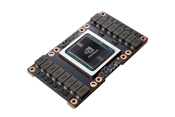
Thanks to Indiana University and The Next Platform, we have a hint of what’s to come with NVIDIA’s future GPU plans, with strong signs that NVIDIA will have a new Tesla accelerator (and underlying GPU) ready for use by this summer.
In an article outlining the installation of Indiana University's Big Red 200 supercomputer – which also happens to be the first Cray Shasta supercomputer to be installed – The Next Platform reports that Indiana University has opted to split up the deployment of the supercomputer in to two phases. In particular, the supercomputer was meant to be delivered with Tesla V100s; however the university has instead opted to hold off on delivery of their accelerators so that they can instead have NVIDIA’s next-generation accelerators, which would make them among the first institutions to get the new accelerators.
The revelation is notable as NVIDIA has yet to announce any new Tesla accelerators or matching GPUs. The company’s current Tesla V100s, based on the GV100 GPU, were first announced back at GTC 2017, so NVIDIA’s compute accelerators are due for a major refresh. However it’s a bit surprising to see anyone other than NVIDIA reveal any details about the new parts, given how buttoned-down the company normally is about such details.
At any rate, according to Indiana University the group expects to have their new accelerators installed by later this summer, with Big Red 200 running in CPU-only mode for now. The Next Platform article goes on to state that the newer accelerators will deliver “70 percent to 75 percent more performance” than NVIDIA’s current V100 accelerators, which assuming it’s accurate, would make for a hefty generational upgrade in performance. Though as always, with multiple modes of compute involved – everything from straight FP32 vector math to tensor operations to low precision operations – the devil is in the details on where those performance gains would most be realized.
In the meantime, NVIDIA’s next GTC event is scheduled for mid-March. So if NVIDIA is planning to launch a new Tesla, then I would certainly expect to see it there.
Source: The Next Platform


38 Comments
View All Comments
Yojimbo - Saturday, February 1, 2020 - link
Who said it's untested. Why make such an assumption? It's been detailed in Research Chip 18.Yojimbo - Saturday, February 1, 2020 - link
I should have said.. Who said it's internal? And I see no reason for Dally to claim in can be used as a drop in replacement for the NVDLA, which he did in an interview with The Next Platform in 2019, when it isn't true. He's not in the part of the company that goes around proselytizing a good deal. If he were to brag about something technical and it weren't true I think it would be looked upon poorly in his circles.Yojimbo - Saturday, February 1, 2020 - link
Ampere will see large changes in its design from Turing. Probably not as large as GCN4 to RDNA, but larger than Volta to Turing. Something along the lines of Pascal to Turing, to just throw something out there. NVIDIA doesn't in general do die shrinks of old architectures, and every time NVIDIA comes out with an architecture on a new node people seem to claim it is going to be a die shrink of the old one. As far as RT cores, it's unlikely the part mentioned in this story, ie the one going in the supercomputer, will have any of them. Somehow NVIDIA will get 70-75% faster performance over Volta, according to the Indiana University supercomputer guy, and it's not going to be entirely from a die shrink from 12 to 7.yeeeeman - Saturday, February 1, 2020 - link
I agree. The timing between Turing and Ampere is a lot more than it is required for a die shrink. They most certainly have changed stuff internally, upgraded rt cores, etc.jabbadap - Monday, February 3, 2020 - link
Yeah it will need more cores. 70% uplift of fp64 crunch from even lowest pcie V100 is 11.9Tflops. Full V100 chip would need to clock 11 900GFlops/(64*84) ~ 2.21GHz. While not out of question clocks for Tesla that's just unlikely.Can't really compare transistor densities between IHVs. But if we take Vega 20 chip, which is 331mm² and has 13230 million transistors. That would make V100 size at 7nm as 331mm² * 21100/13230 ~ 528mm². So there could be a bit more room for more cudas as I don't think they will make much over 600mm² chips at the 7nm EUV process.
Spunjji - Monday, February 3, 2020 - link
I thought that a die shrink of and older architecture was exactly how Nvidia went about transitioning to new nodes after the disaster that was NV30? They only seem to have stopped that approach fairly recently with Pascal, though my understanding is that was still less of a change from Maxwell than Turing is from Pascal.Unless I'm misreading you and you're simply pointing out that they never release an entirely new range that is *just* a die shrink, which is fair.
Agreed that RT cores are unlikely on a supercomputer chip, though. Perhaps this chip will bear a similar relationship to the Ampere consumer cards that Volta does to consumer Turing.
Yojimbo - Monday, February 3, 2020 - link
The change NVIDIA made was to not aggressively pursue new process nodes. They generally wait longer than AMD to introduce products on a new node. But they do not take existing architectures and shrink it to a new node. Pascal was a significant change from Maxwell, Kepler was a significant change from Fermi. Before that we are getting into some ancient history.I'm not sure what you mean by distinguishing "just" a die shrink. That's what people necessarily mean when they say "The new architecture is not really new it is a die shrink of the old one". In any case, don't think there's any reason to believe that NVIDIA holds back their big changes away from when they change nodes. Kepler was a massive change from Fermi and was on a new node. Judging by the odd release of the architecture and the rejiggering of their architectures NVIDIA did at the time (Maxwell 1 and Maxwell 2, adding Pascal into the roadmap and shifting features around), I think Maxwell was originally planned to be on a new node but that node ended up not working out because planar FETs hit a wall.
jabbadap - Tuesday, February 4, 2020 - link
Well yeah Maxwell should have been on TSMC 20nm, but that node failed miserably. So Maxwell were stript down from fp64 compute and released on old 28nm node. Pascal gp100 was then what big Maxwell should have been, so it was more like an evolution from Maxwell rather than hole new Arch. So I would not call it very significant, i.e. Kepler to Maxwell is much larger change as is Pascal to Turing.Well now, as Turing is more like an evolution of Volta, is it really time for an hole new architecture yet? Or will Nvidia do another evolution with Ampere and die shrink Volta/Turing shaders to 7nm, amplify RT(maybe smaller SMs i.e. 32cc instead of 64cc thus more RT cores), modify Tensors(BFloat16) and call it a day.
Smell This - Friday, January 31, 2020 - link
It says 'Ampere' at the link but it's a bit fuzzy.**The original plan was to outfit the system with Nvidia V100 GPUs, which would have brought its peak performance to around 5.9 petaflops.**
It goes on to state the original 672 dual-socket nodes -- “Rome” Epyc 7742 processors from AMD -- will bring "... additional nodes online" this Summer, and expected to deliver close to 8 petaflops.
**The newer silicon is expected to deliver 70 percent to 75 percent more performance than that of the current generation** but **ended up buying a smaller number of GPUs**
??
Yojimbo - Saturday, February 1, 2020 - link
What's fuzzy? Can you provide some commentary to let people know what you are talking about?