Intel 7nm Delayed By 6 Months; Company to Take “Pragmatic” Approach in Using Third-Party Fabs
by Ryan Smith on July 23, 2020 10:00 PM EST
While today second quarter earnings report from Intel represented a high-water mark for the company amid booming sales and revenues, unfortunately not everything disclosed today was good news from the company. As part of Intel’s quarterly earnings presentation, the company announced that their under-development 7nm manufacturing process has suffered a six month delay due to a defect in the process. As a result, the first consumer products aren’t due until at least late 2022, leaving Intel with 10nm as their best in-house manufacturing process for the next couple of years.
But even more important than that, the delay has spurred some soul searching within Intel, driving the company to pivot on its manufacturing plans and open the door to using third-party fabs for a much broader segment of its products. Going forward, the company will be taking what CEO Bob Swan and other leadership are calling a “pragmatic” approach, looking at both in-house and third-party fabs and using those fabs that make sense for the company and the product in question. And while the company has not announced any specific plans to outsource production – they are looking at it for products in the 2022-and-later timeframe – it would be hard to overstate how dramatic of a shift this is for the industry, and for a company that even five years ago was the world’s leader in silicon lithography manufacturing.
7nm Delayed By Six Months
But before we get too far into Intel’s future plans, let’s talk about the past and the present, and how those are driving Intel’s decision to look towards outside fabs. Ever since Intel’s 10nm process suffered repeated delays, Intel’s plan to get the company’s manufacturing side back on track was to nail the development of their 7nm process. The goal was to deliver 7nm on time – making up for the time lost from the 10nm delays – getting a solid process out that Intel could quickly ramp up, retaking the lead in the race to sustain Moore’s Law. A side-effect of this plan would have been that 10nm was to be a relatively short-lived process, allowing Intel to get off of the troubled process rather quickly and on to the more reliable 7nm process.
Unfortunately for Intel, developing their 7nm process has not gone to plan. As revealed in today’s call, 7nm yields are roughly a full year behind schedule – that is, Intel expects it to take another year to get yields to where they wanted them for Q2 of 2020. As a result, the company has needed to push back the bulk of its 7nm product schedule by 6 months. The first 7nm client CPUs are now not expected before late 2022 or early 2023. Meanwhile the first 7nm server part is not expected until the first half of 2023.
The only 7nm part that remains (roughly) on schedule at this point is Ponte Vecchio, Intel’s Xe-HPC GPU that will be going into the Aurora supercomputer. That is expected to ship in late 2021 or early 2022, and even then Intel is evaluating whether to move the manufacturing of some of Ponte Vecchio’s parts to third-party fabs.
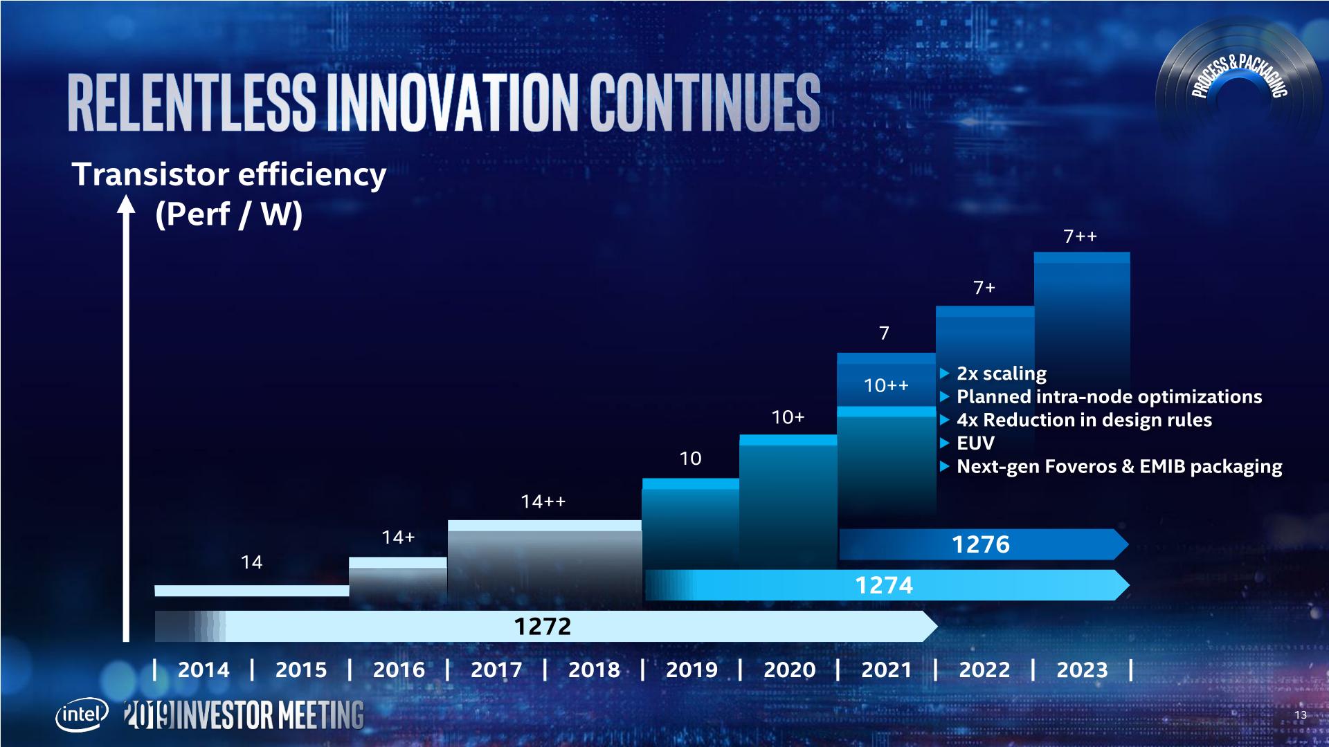
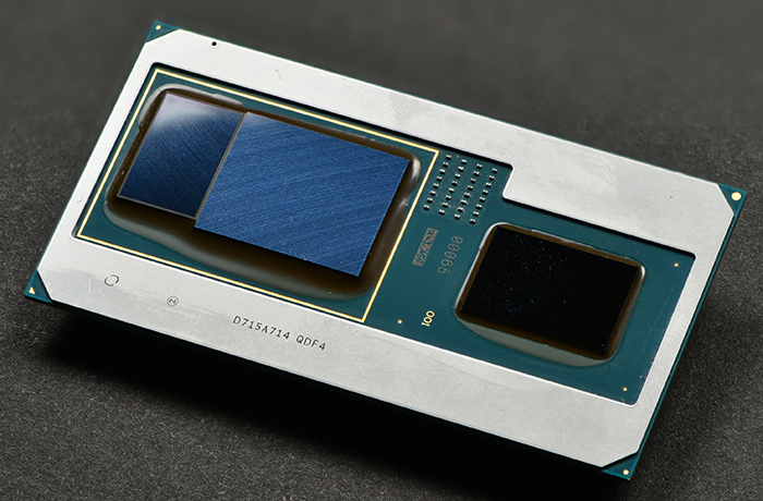
For Reference: Intel's Fab Schedule Circa May 2019
The good news, at least, is that despite all of this, Intel believes that they have a good grasp on the problem. With Swan describing the problem as a “defect mode” that was reducing yields, Intel has found the root cause of the issue and is moving to fix it, stating that that the company doesn’t believe that there are any fundamental roadblocks in their 7nm process. So as Intel’s current plans go, the company is still all-in on 7nm, and baring further issues, it’s going to become the cornerstone of their technology in 2023 when it begins volume shipping.
None the less, a six month delay is still a six month delay, and it comes at a time when Intel can ill afford it. Intel’s repeated 10nm problems set the company back years, and the ramifications to Intel’s product lines are ongoing as they continue to ship 14nm desktop and server processors. Meanwhile, though not wholly comparable in terms of node size, fab rival TSMC is set to start shipping 5nm parts this year, extending their lead over Intel and giving TSMC’s customers a leg-up in terms of things like power efficiency and die sizes. At the end of the day Intel has already been down this road once before with 10nm, and they’re intent on not repeating the same mistakes.
Being Pragmatic Means Knowing When to Yield
As a result of the 7nm delay, going forward Intel will be taking what Swan is calling a “pragmatic” approach in selecting what foundries to use. Intel will no longer be limiting themselves to near-exclusive use of their own fabs, and instead the company will be taking the capabilities (and costs) of third-party fabs into the equation. At the end of the day Intel still wants to produce market-leading chips, and they are now willing to use third-party fabs to accomplish this.
We will continue to invest in our future process technology roadmap, but we will be pragmatic and objective in deploying the process technology that delivers the most predictability and performance for our customers, whether that be our process, external foundry process or a combination of both.
-Intel CEO Bob Swan
While Intel isn’t committing to any specific manufacturing plans today, the message from Intel is clear: they will do what they need to in order to deliver new products according to their release roadmap. This means relying on third-party fabs as a contingency plan and leaving virtually every option on the table, including manufacturing a product entirely at a third-party fab if that is truly the best option. Ultimately, the question Intel is facing is how much should they rely on their 7nm fabs, and how much should they rely on third parties.
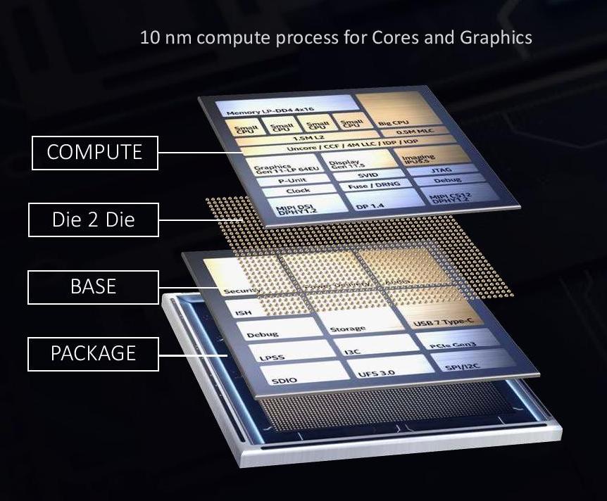
Meanwhile, underpinning this newfound philosophy of flexibility are Intel’s recent developments in what the company is terming “disaggregated die” technologies like EMIB and Foveros. These multi-chip packaging technologies, which have been rolled out in products like Kaby Lake-G and Intel’s new Core-L “Lakefield” processors, allow for multiple dissimilar dies to be used on a single package. In Lakefield’s case, that was accomplished by layering a 10nm compute die on top of a 22nm I/O die, allowing Intel to make the performance critical parts of the chip on the relatively expensive 10nm process, while non-critical parts were built on an extremely power efficient version of 22nm.
Lakefield, in turn, is the first of what will be many products from Intel using this technology. By gluing chips together Intel can not only better manage yield issues – defects are far less disruptive when they impact a small chiplet instead of a large monolithic die – but it means Intel can continue to mix-and-match different process nodes. And not just different Intel process nodes, but third-party process nodes as well.
We’ve already seen a very small taste of this with Kaby Lake-G, which used a GlobalFoundries-built GPU with an Intel-built CPU, albeit on a very coarse scale with minimal integration. But going forward intel’s flexibility plans mean they need to do it on a much larger and finer-grained scale. The upshot is that based on Lakefield there seems to be little doubt Intel can do this – which fab the chips come from shouldn’t have much of an impact on packaging – and instead it’s a question of how much of it Intel does. It’s clear that no matter what, Intel has to go the chiplet route for future products, as chiplets are what will enable Intel’s fab flexibility. But which of those chiplets will be Intel-made, and which of them will be made by third-party fabs? Intel will be spending the next couple of years figuring out just that.
Finally, it bears mentioning that none of this would even be possible without Intel’s other recent pivot towards divorcing product designs from process nodes. The company’s traditional vertically-integrated design philosophy has delivered a lot of excellent products over the years, but Intel has been feeling the pain of this decision since 10nm was delayed, and with it the use of their newer Sunny Cove CPU architecture. Intel has only recently gained the ability to port an architecture to multiple process nodes, and it’s clear they are going to be heavily relying on that ability as part of any third-party chipmaking.
But First, Ponte Vecchio
While the bulk of Intel’s announcement today deals with products set for the 2023 timeframe, the company has also publicly commented on what it means for their very first 7nm product, Ponte Vecchio. The Xe-HPC GPU is the flagship of Intel’s Xe GPU efforts, and Ponte Vecchio chips are a fundamental building block of the forthcoming Aurora Supercomputer. But even more importantly for Intel right now are delivery dates: Aurora is scheduled to be delivered in 2021, a year before Intel is set to deliver their first high-volume consumer 7nm parts. Ponte Vecchio is an extremely important product for Intel, and they only have a limited amount of time left to work on it.

As a result, Intel has confirmed that the company is also reevaluating what fabs are used for the various parts of Ponte. Curiously, Intel has stated that the chip was always going to use a mix of first-party and third-party fabs, though I wonder if Intel is being a bit fast & loose there by including the HBM memory (which Intel doesn’t produce) in that assessment. At any rate, even if you exclude the memory, that still leaves the I/O base die, the connectivity chips, and the GPU itself as separate dies, any of which could theoretically be shuffled off to a third party fab.
To be sure, like the other announcements today Intel is sharing their specific manufacturing plans – and it’s likely Intel hasn’t even made a final decision on where to make the various chips. But at the same time Intel is making it clear that they are considering all of their options. The Aurora supercomputer was already scrapped once (when it was planned to be a Xeon Phi system), so Uncle Sam is going to be eager to get his $500M supercomputer, and Intel in turn may need to swallow some of its pride to make it happen.
Many Unknowns, but Intel’s Transformation Is Certain
Wrapping things up, while there are a lot of unknowns and things left to be determined in Intel’s plan, there is one thing that is certain: no matter what happens, Intel will be transforming. At a minimum they will be transforming from a company that relies on monolithic dies to a company that embraces multi-chip packages, and depending on how things go with 7nm, they may also be transforming into a company that farms out much of its chip production to third parties. This is nothing short of a remarkable change for a company that ruled the world of chipmaking not even half a decade ago.
But it’s a remarkable change that needs to happen. Though undoubtedly a hard pill for Intel to swallow, Intel’s 7nm delay poses a significant risk to a company that is already bracing for hard times from their 10nm delay. So something needed to change, if only so that Intel has a contingency plan in place should 7nm slip yet again.
At the end of the day what happens next is still up in the air. Intel has decisions to make, and perhaps most importantly of all, Intel’s process technology team is facing a do-or-die situation with 7nm. Intel has invested a great deal in their 7nm process, and for both profit and product reasons, they would certainly prefer to use that. This means that if Intel can keep 7nm on track, then what is now just a contingency plan will likely remain just that.
But regardless of what happens, it’s clear that Intel can no longer bet the house on themselves. Silicon lithography is only getting harder, and a very mortal Intel has to prepare for the possibility that it's a race they may not win.


208 Comments
View All Comments
HomelessHardware - Sunday, July 26, 2020 - link
Seems an easy business arrangement. Intc has billions in cash. They pay for the new plants. Provides a 5 year agreement to purchase all chips from the plants.This idea that tsmc, a 3rd party manufacturing company, would turn down the largest chip designer in the world because they have it good with amd is ridiculous. Does anyone have memory of amd beyond the last 3 years?
dotjaz - Monday, July 27, 2020 - link
Your logic is simply laughable. Intel has it's own capacity, its demand is not long term at all. They simply won't sign such a WSA. Only stupid people would assume Intel would sign that.vFunct - Wednesday, July 29, 2020 - link
Intel has zero fab capacity at 7nm. TSMC does.If Intel offered TSMC $20 billion, TSMC would gladly build a new 7nm fab just for Intel, because that's their business model: to sell wafer capacity.
dotjaz - Friday, July 31, 2020 - link
What a stupid comment. TSMC sells capacity not Fabs.Spunjji - Monday, August 3, 2020 - link
vFunct and HomelessHardware here providing the thrilling armchair analysis of "have big money, get big fab built". It's not that simple, and that's not what's happening.dotjaz - Sunday, July 26, 2020 - link
I doubt they would be stupid enough to do a WSA, both Intel and TSMC are smarter than that. It will anger TSMC's other customers and also Intel will have to meet the quota like AMD had to for years.JCB994 - Friday, July 24, 2020 - link
You ever build fabs in Asia? I used to work for Samsung and if they decided to build a fab, tools are being pushed in around 6-9 months later...assuming they can get the tools that fast. Not saying the fab is finished in that timeframe but if a HEPA is in place, the tool is in place underneath. Plastic sheathing is fine for walls.eek2121 - Friday, July 24, 2020 - link
The building isn’t the issue. The equipment is.FullmetalTitan - Friday, July 24, 2020 - link
I think the limiting factor here depends on what node they are pushing to a 3rd party. If they want anything from the 7/10nm designs, they need EUV capacity which is not a next day type of order. Otherwise, yeah I have seen some fast and dirty install and ramp up work done in fabs. If they are going to move an older, defect tolerant device to 3rd party, they could get away with the condensed time frame on expansionCalin - Saturday, July 25, 2020 - link
Intel's 14nm is close to the best there is, and Intel is on the third of fourth iteration of 14nm.Taking everything into account, moving 14nm production to a different maker (like Samsung, TSMC, ...) would probably double their costs - not to take into account scraping good-enough production capacity.
So, what Intel needs is 7nm (or better) capacity (and a LOT of it), not 10nm or older. Just a bit of 7nm production capacity would be counter-productive - everyone would want the BEST there is, and expect a huge discount on the current products made on the older lithography nodes.