TSMC: We have 50% of All EUV Installations, 60% Wafer Capacity
by Dr. Ian Cutress on August 27, 2020 12:00 PM EST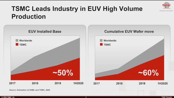
One of the overriding central messages to TSMC’s Technology Symposium this week is that the company is a world leader in semiconductor manufacturing, especially at the leading edge process technology. To further hit the message home, TSMC showcased a slide indicating where it stands in relation to others: by using a combination of public ASML statements and their own internal purchase sheets, TSMC predicts that they have ~50% of all the active EUV machines installed worldwide. Beyond that, the company also has a number of ~60% for cumulative EUV wafer production.
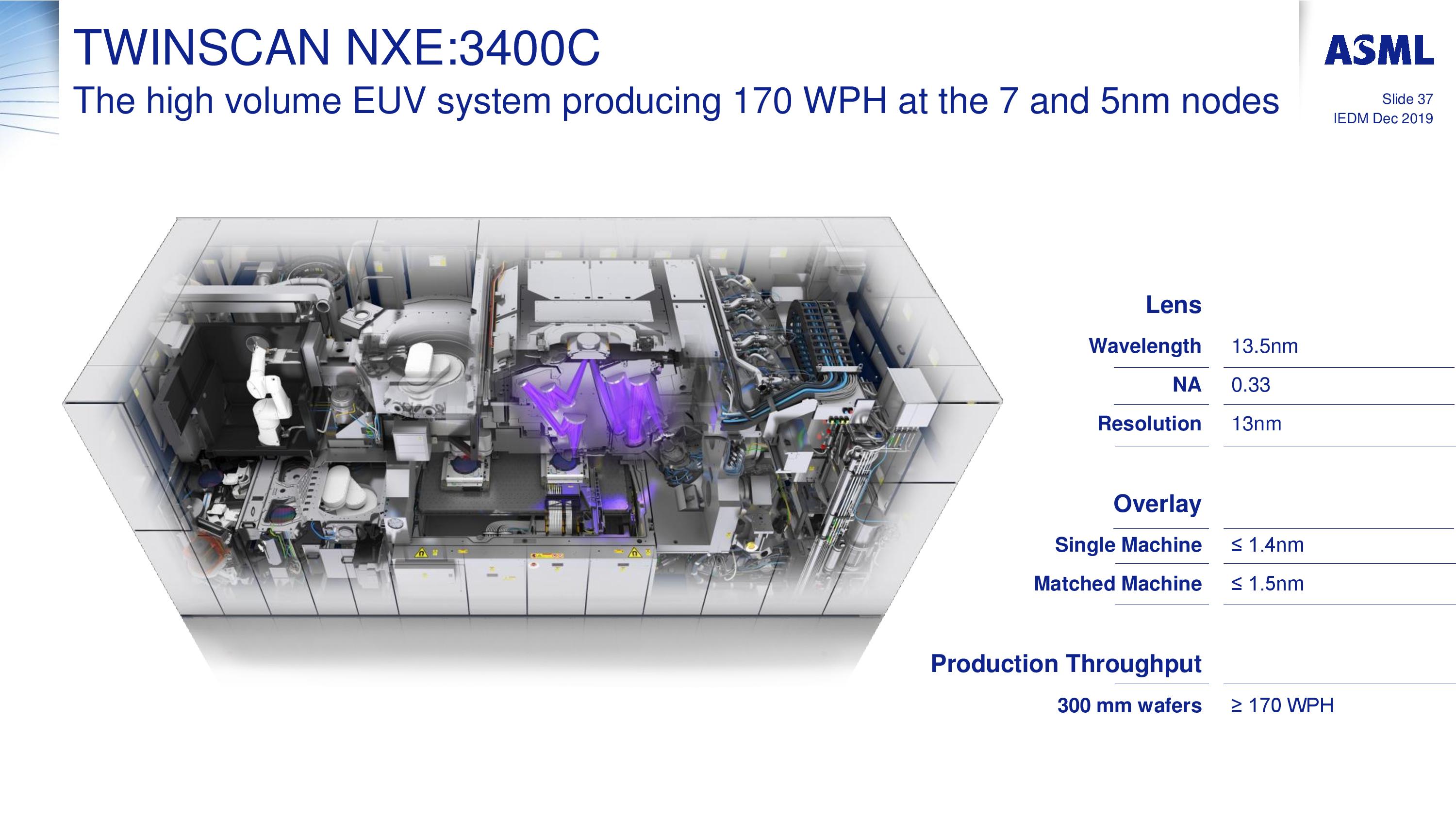
Current known public EUV processes from the big fabs include TSMC’s 7+ and N5, as well as Samsung’s 7LPP (and anything below), with Intel’s EUV efforts only entering in its own 7nm portfolio next year. Anything beyond these processes at the leading edge will continue to extend EUV use. EUV machines typically have a lower throughput, anywhere from 120-175 wafers per hour, than regular DUV machines which can reach 275 wph on the latest versions, however since 1 layer of EUV typically replaces 3-4 layers of DUV, the throughput is higher, but nonetheless the desire to scale out to multiple EUV machines to increase the physical number of wafers is a keen target for these foundries.
The only company that makes EUV machines is ASML, and the company publically announces how many machines it sells each year. The details are as follows:
| ASML's EUV Shipments | ||||||||||||||||||
| 2015 | 2016 | 2017 | 2018 | 2019 | 2020 | 2021 | ||||||||||||
| Actual | 2 | 4 | 10 | 3 | 4 | 5 | 6 | 4 | 7 | 7 | 8 | 4 | 9 | - | - | - | ||
| Target | - | - | - | 20 | 30 | 35 | 45-50 | |||||||||||
| 2018 and beyond is split per quarter for actual shipped numbers Data taken from ASML's Financial Reports |
||||||||||||||||||
Note that each year so far, ASML hasn’t quite hit its targets, but has done near enough, although sales in Q1 2020 were lower than I would expect, indicating that by end of Q2 2020, ASML has only shipped 13 out of the proposed 35 systems. These numbers include all the different types of Twinscan NXE machines that ASML has built, with the more recent ones having better throughput (and sometimes the older ones get retrofitted). As of the end of Q2 2020, we predict that ASML has shipped around 71 of these EUV machines, and will likely hit 90 by the end of 2020. Some observers have noted that ASML may have a backlog of as many as 49 EUV scanner orders, even with these shipment targets.

If ASML has shipped 71 machines, that would mean, according to TSMC’s numbers, the company has around 30-35. Note that TSMC’s numbers are for ‘Installed EUV’ machines – we learned from our trip to GlobalFoundries in Q1 2018 that it takes up to 6 months from getting the parts to calibrating the machine for use. At present, some of these foundries therefore have EUV machines sitting around waiting to be installed, or in the case of Intel, perhaps only in use for early testing or pre-risk trials. We know that GlobalFoundries had two early EUV machines, installed one, but ended up selling both when it decided not to pursue leading edge 7nm, and SMIC ordered one but as far as we know it wasn’t installed due to restrictions imposed by the US.
As TSMC grows its Fab 18 for N5 production, and ramps its EUV integration, it will be interesting to see if TSMC is ever limited by the number of machines it has. At some point Intel is going to want to buy a number when it deploys its 7nm processes (I’ve seen predictions that Intel has at least ~10 machines already, but I can’t confirm that) as well, so there might be a tussle for who gets their order delivered first.
One thing is for sure however, ASML is sitting pretty right in the middle with a monopoly on everything. I still have an invite to visit one of their EUV machine factories in Connecticut, which when the COVID mess is all over I intend to follow up on. It should be exciting.
Related Reading
- SMIC Details Its N+1 Process Technology: 7nm Performance in China
- GlobalFoundries Stops All 7nm Development: Opts To Focus on Specialized Processes
- Intel 7nm Delayed By 6 Months; Company to Take “Pragmatic” Approach in Using Third-Party Fabs
- TSMC: N7+ EUV Process Technology in High Volume, 6nm (N6) Coming Soon
- TSMC: 3nm EUV Development Progress Going Well, Early Customers Engaged
- TSMC’s 5nm EUV Making Progress: PDK, DRM, EDA Tools, 3rd Party IP Ready
- ASML’s First Multi-Beam Inspection Tool for 5nm
- TSMC Expects 5nm to be 11% of 2020 Wafer Production (sub 16nm)
- ‘Better Yield on 5nm than 7nm’: TSMC Update on Defect Rates for N5
- TSMC Details 3nm Process Technology: Full Node Scaling for 2H22 Volume Production
- TSMC Confirms Halt to Huawei Shipments In September


32 Comments
View All Comments
J0S3R - Thursday, August 27, 2020 - link
Do we know how those machines are distributed amongst TSMC sites worldwide? Curious how diversified they are against risks in Taiwan both natural (such as earthquakes) and unnatural (such as China).Ian Cutress - Thursday, August 27, 2020 - link
That should be as simple as asking which Fabs at TSMC do N7+, N5, or are leading-edge R&D.Gondalf - Saturday, August 29, 2020 - link
In your article you mean "exposures" and not "layers"....i believe.The number of layers is not process related but a Foundry choice to address customers SOC complexity demand. Another matter are the exposures to have a good layer.
Modern DUV based silicon (7nm class) require between three and four exposures on critical layers.
The real problem is that a true 5nm a single patterning of EUV could be not enough on critical layers with NA = 0.33. Looking at TSMC 5nm we can see that it is pretty conservative and the density absolutely is not a record this time. Intel is much more aggressive with 7nm and sure they need of two EUV exposures on critical layers.
IMO this the reason of Intel delay on 7nm or this is why they will mix a less advanced TSMC/Samsung 5nm process with their leading edge (but expensive) 7nm.
Looking at Ponte Vecchio, Intel will utilize their 7nm for cache to have a strong sram footprint reduction, leaving dirty logic to Foundries.
Honestly these ASML machines are embarassing, they do not meet the foundries specifics, and i have suspect 5nm output will not be large as 7nm. 3nm looks a real disaster, 2nm a low output process for premium applications.
Any news about the lack of 24/7 availability of these EUV scanners?? Are already true the frequents stops of the scanners due lack of reliability in the long run? This could be a limiting factor for large volume or the reason why TSMC orders a so large number of scanners (backup machines).
Santoval - Saturday, August 29, 2020 - link
"Looking at TSMC 5nm we can see that it is pretty conservative and the density absolutely is not a record this time. Intel is much more aggressive with 7nm and sure they need of two EUV exposures on critical layers."Actually the projected transistor density of TSMC at 5nm and Intel at 7nm is not that different. Intel is expected to be more aggressive, sure, but not *much* more aggressive. They are targeting a doubling of density at 7nm versus 10nm So, for the highest density cell library of both nodes (which is used for uncore and I/O parts of the doe, *not* for logic) they will move from ~100 million transistors per mm² (MTr/mm²) to ~200 MTr/mm².
TSMC are targeting a transistor density of 173.1 MTr/mm² in the first (N5) iteration of their 5nm node (per SemiWiki anyway, see link below), but they will also release a second denser 5nm node iteration a few quarters later, as they always do, that will get even closer to Intel's 7nm node in density. While that might not be record setting compared to Intel's targets its release will definitely set a density record, by far, since Intel's 7nm node is not anywhere near ready and will rather compete with TSMC's 3nm node... which will be quite denser.
The company that is very conservative at 5nm is actually Samsung. Their 5LPE node will have a density of a mere 126.5 MTr/mm², which is barely denser than TSMC's (partly EUV using) 7nm+/7FFP node. That's because Samsung at 5nm are basically switching from DDB (double diffusion break) to SDB (single diffusion break) and that's it. That's the same change TSMC did with the second gen 7nm+ iteration of their 7nm node to increase density. So Samsung's 5nm node is basically going to be a slightly denser 7nm+ node. The above assume that the data of this article are valid :
https://semiwiki.com/semiconductor-manufacturers/s...
Santoval - Saturday, August 29, 2020 - link
edit : "which is used for uncore and I/O parts of the doe ---> *die*"dotjaz - Monday, August 31, 2020 - link
N5P is not denser. And while Intel claims to have better density, there's no chip in existence to verify that.dotjaz - Monday, August 31, 2020 - link
What a stupid rant. Intel's 7nm is the inferior process.flgt - Thursday, August 27, 2020 - link
Yeah, that’s a great question. I know that’s some bragging rights for their marketing department but it’s got to be raising some eyebrows around the world. Everyone is cheering on Intel’s downfall but we may not want all our eggs in the TSMC/ASML basket in 5 years.FunBunny2 - Thursday, August 27, 2020 - link
"all our eggs in the TSMC/ASML basket in 5 years"as the author says, ASML currently has a monopoly on these kind of machines, so questions:
1 - are there other vendors for current/DUV machines?
2 - are there other vendors for EUV machines?
IOW, the bottleneck isn't TSMC. if it is true that ASML is the sole source for EUV (and, perhaps, best DUV?), it makes little difference which foundry has the machines, from a customer/cost point of view. since, I'd wager, capital amoritization is the driving cost of wafers, ASML's 'tax' will be built in wherever the wafer comes from.
Tomatotech - Thursday, August 27, 2020 - link
These machines are insanely complex. They cost nearly $100 million each and are just one tool in a long chain of tools. As you saw in the article there are only a few humans in the world with the technical skills to set them up. Several machines are sitting unused waiting for this tiny group of humans to get round to setting them up.The tech is insane - these machines work by throwing a tiny droplet of molten tin in the air on an excessively precise trajectory then vaporising it with intense lasers, collecting the light from the plasma (which damages everything it touches) and focusing it to make circuits tinier than anything made before. There are several stages, each of which loses 95%-98% of the power, so from a 500,000w wall supply, only 200w of light is output, and only about 4w of light actually arrives at the wafer to do the masking / lithography work.
ASML is basically supported by a joint agreement between every large chipmaker on the planet. It's not possible to have a second company making these machines, the capacity just isn't there and the expense is too high. Maybe in a few years time when ASML has moved onto creating whatever comes after EUV.