AMD Zen 3 Ryzen Deep Dive Review: 5950X, 5900X, 5800X and 5600X Tested
by Dr. Ian Cutress on November 5, 2020 9:01 AM ESTSection by Andrei Frumusanu
The New Zen 3 Core: High-Level
As we dive into the Zen3 microarchitecture, AMD made a note of their journey of the last couple of years, a success-story that’s been started off in 2017 with the revolutionary Zen architecture that helped bring AMD back to the competitive landscape after several sombre years of ailing products.
The original Zen architecture brought a massive 52% IPC uplift thanks to a new clean-sheet microarchitecture which brought at lot of new features to the table for AMD, introducing features such as a µOP cache and SMT for the first time into the company’s designs, as well as introducing the notion of CPU core-complexes with large (8MB at the time) L3 caches. Features on a 14nm FinFET process node, it was the culmination and the start-off point of a new roadmap of microarchitectures which leads into today’s Zen3 design.
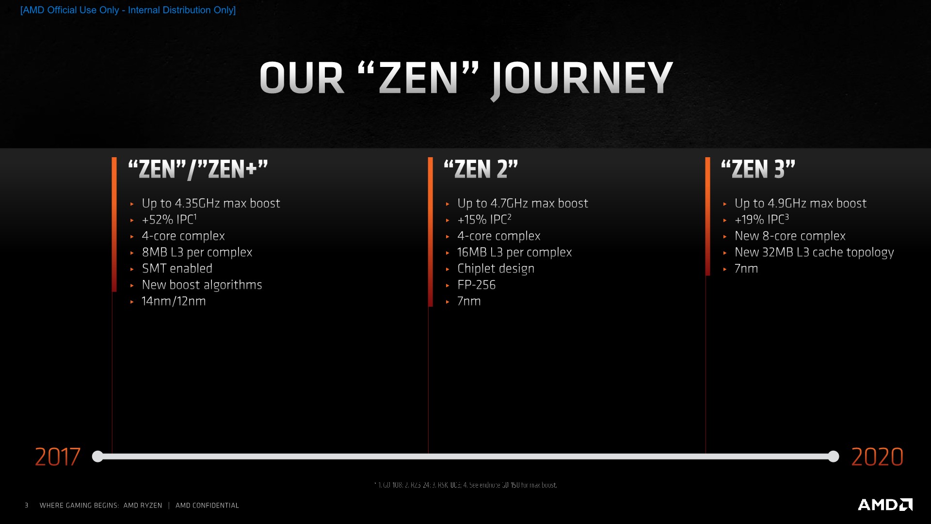
Following a minor refresh in the form of Zen+, last year’s 2019 Zen2 microarchitecture was deployed into the Ryzen 3000 products, which furthered AMD’s success in the competitive landscape. Zen2 was what AMD calls a derivative of the original Zen designs, however it contained historically more changes than what you’d expect from such a design, bringing more IPC increases than what you’d typically see. AMD saw Zen2 as a follow-up to what they had learned with the original Zen microarchitecture, fixing and rolling out design goal changes that they had initially intended for the first design, but weren’t able to deploy in time for the planned product launch window. AMD also stated that it enabled an opportunity to bring some of the future Zen3 specific changes were moved forward into the Zen2 design.
This was also the point at which AMD moved to the new chiplet design, leveraging the transition to TSMC’s new 7nm process node to increase the transistor budget for things like doubling the L3 cache size, increasing clock speeds, and vastly reducing the power consumption of the product to enable aggressive ramp in total core counts both in the consumer space (16-core Ryzen 9 3950X), as well as in the enterprise space (64-core EPYC2 Rome).
Tying a cutting-edge high-performance 7nm core-complex-die (CCD) with a lower cost 12/14nm I/O die (IOD) in such a heterogenous package allowed AMD to maximise the advantages and minimise the disadvantages of both respective technologies – all whilst AMD’s main competitor, Intel, was, and still is, struggling to bring out 10nm products to the market. It was a technological gamble that AMD many times has said was made years in advance, and has since paid off plenty.
Zen 3 At A Glance
This brings us to today’s Zen3 microarchitecture and the new Ryzen 5000 series. As noted earlier, Mark Papermaster had mentioned that if you were to actually look at the new design from a 100,000-foot level, you’d notice that it does look extremely similar to previous generation Zen microarchitectures. In truth, while Zen3 does share similarities to its predecessors, AMD’s architects started off with a clean-sheet design, or as they call it – “a ground-up redesign”. This is actually quite a large claim as this is a quite enormous endeavour to venture in for any company. Arm’s Cortex-A76 is the most recent other industry design that is said to have been designed from scratch, leveraging years of learning of the different design teams and solving inherent issues that require more invasive and large changes to the design.
Because the new Zen3 core still exhibits quite a few defining characteristics of the previous generation designs, I think that AMD’s take on a “complete redesign” is more akin to a deconstruction and reconstruction of the core’s building blocks, much like you’d dismantle a LEGO set and rebuild it anew. In this case, Zen3 seems to be a set-piece both with new building blocks, but also leveraging set pieces and RTL that they’ve used before in Zen2.
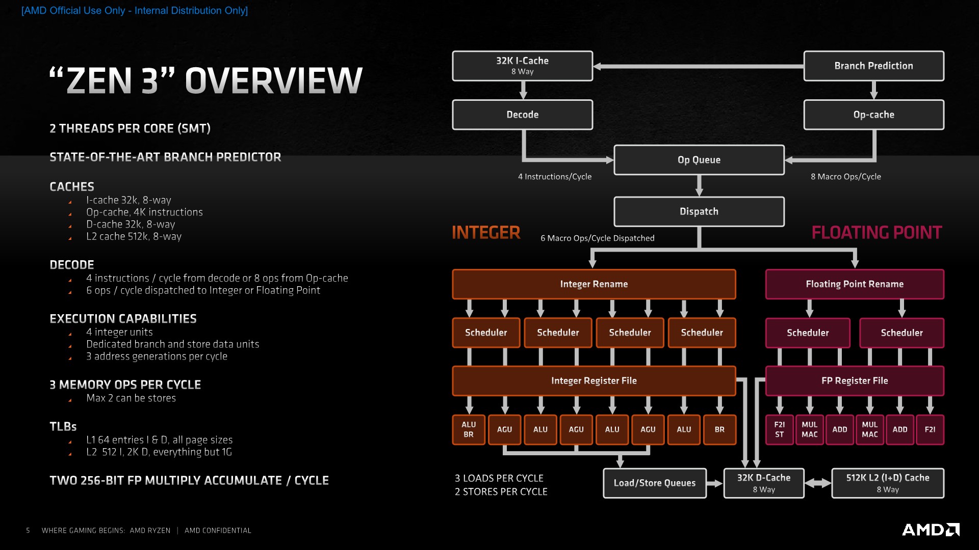
Whatever the interpretation of a “clean-sheet” or “complete redesign” might be, the important take is that Zen3 is a major overhaul in terms of its complete microarchitecture, with AMD paying attention to every piece of the puzzle and trying to bring balance to the whole resulting end-design, which comes in contrast to a more traditional “derivative design” which might only touch and see changes in a couple of the microarchitecture’s building blocks.

AMD’s main design goals for Zen3 hovered around three main points:
- Delivering another significant generational single-threaded performance increase. AMD did not want to be relegated to top performance only in scenarios where workloads would be spread across all the cores. The company wanted to catch up and be an undisputed leader in this area to be able to claim an uncontested position in the market.
- Latency improvements, both in terms of memory latency, achieved through a reduction in effective memory latency through more cache-hits thanks to the doubled 32MB L3 that an individual core can take advantage of, as well as core-to-core latency which again thanks to the consolidated single L3 cache on the die is able to reduce long travel times across the dies.
- Continuing a power efficiency leadership: Although the new Zen3 cores still use the same base N7 process node from TSMC (although with incremental design improvements), AMD had a constraint of not increasing power consumption for the platform. This means that any new performance increases would have to come through simultaneous power efficiency improvements of the microarchitecture.
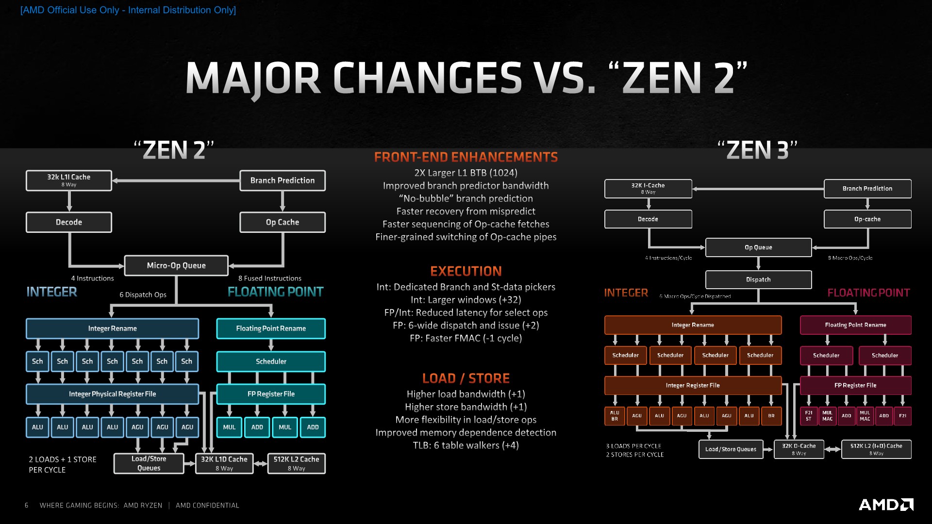
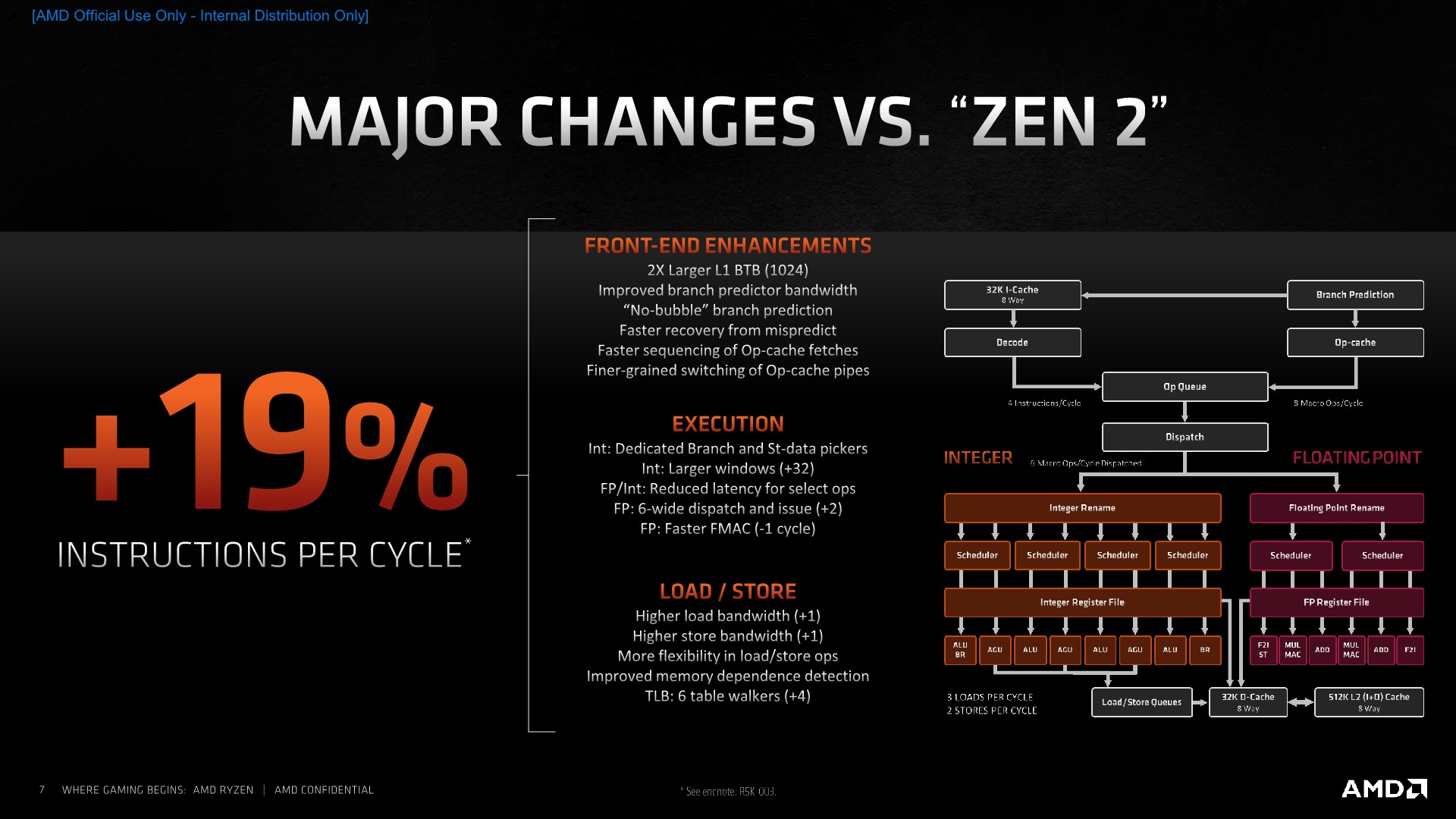
The culmination of all the design changes AMD has made with the Zen3 micro-architecture results in what the company claims as a 19% average performance uplift over a variety of workloads. We’ll be breaking down this number further into the review, but internal figures show we are matching the 19% average uplift across all SPEC workloads, with a median figure of 21%. That is indeed a tremendous achievement, considering the fact that the new Ryzen 5000 chips clock slightly higher than their predecessors, further amplifying the total performance increase of the new design.


339 Comments
View All Comments
TheinsanegamerN - Tuesday, November 10, 2020 - link
However AMD's boost algorithim is very temperature sensitive. Those coolers may work fine, but if they get to the 70C range you're losing max performance to higher temperatures.Andrew LB - Sunday, December 13, 2020 - link
Blah blah....Ryzen 5800x @ 3.6-4.7ghz : 219w and 82'c.
Ryzen 5800x @ 4.7ghz locked: 231w and 88'c.
Fractal Celsius+ S28 Prisma 280mm AIO CPU cooler at full fan and pump speed
https://www.kitguru.net/components/cpu/luke-hill/a...
If you actually set your voltages on Intel chips they stay cool. My i7-10700k @ 5.0ghz all-core locked never goes above 70'c.
Count Rushmore - Friday, November 6, 2020 - link
It took 3 days... finally the article load-up.AT seriously need to upgrade their server (or I need to stop using IE6).
name99 - Friday, November 6, 2020 - link
"AMD wouldn’t exactly detail what this means but we suspect that this could allude to now two branch predictions per cycle instead of just one"So imagine you have wide OoO CPU. How do you design fetch? The current state of the art (and presumably AMD have aspects of this, though perhaps not the *entire* package) goes as follows:
Instructions come as runs of sequential instructions separated by branches. At a branch you may HAVE to fetch instructions from a new address (think call, goto, return) or you may perhaps continue to the next address (think non-taken branch).
So an intermediate complexity fetch engine will bring in blobs of instructions, up to (say 6 or 8) with the run of instructions terminating at
- I've scooped up N or
- I've hit a branch or
- I've hit the end of a cache line.
Basically every cycle should consist of pulling in the longest run of instructions possible subject to the above rules.
The way really advanced fetch works is totally decoupled from the rest of the CPU. Every cycle the fetch engine predicts the next fetch address (from some hierarchy of : check the link stack, check the BTB, increment the PC), and fetches as much as possible from that address. These are stuck in a queue connected to decode, and ideally that queue would never run dry.
BUT: on average there is about a branch every 6 instructions.
Now supposed you want to sustain, let's say, 8-wide. That means that you might set N at 8, but most of the time you'll fetch 6 or so instructions because you'll bail out based on hitting a branch before you have a full 8 instructions in your scoop. So you're mostly unable to go beyond an IPC of 6, even if *everything* else is ideal.
BUT most branches are conditional. And good enough half of those are not taken. This means that if you can generate TWO branch predictions per cycle then much of the time the first branch will not be taken, can be ignored, and fetch can continue in a straight line past it. Big win! Half the time you can pull in only 6 instructions, but the other half you could pull in maybe 12 instructions. Basically, if you want to sustain 8 wide, you'd probably want to pull in at least 10 or 12 instructions under best case conditions, to help fill up the queue for the cases where you pull in less than 8 instructions (first branch is taken, or you reach the end of the cache line).
Now there are some technicalities here.
One is "how does fetch know where the branches are, to know when to stop fetching". This is usually done via pre-decode bits living in the I-cache, and set by a kinda decode when the line is first pulled into the I-cache. (I think x86 also does this, but I have no idea how. It's obviously much easier for a sane ISA like ARM, POWER, even z.)
Second, and more interesting, is that you're actually performing two DIFFERENT TYPES of prediction, which makes it somewhat easier from a bandwidth point of view. The prediction on the first branch is purely "taken/not taken", and all you care about is "not taken"; the prediction on the second branch is more sophisticated because if you predict taken you also have to predict the target, which means dealing BTB or link stack.
But you don't have to predict TWO DIFFERENT "next fetch addresses" per cycle, which makes it somewhat easier.
Note also that any CPU that uses two level branch prediction is, I think, already doing two branch prediction per cycle, even if it doesn't look like it. Think about it: how do you USE a large (but slow) second level pool of branch prediction information?
You run the async fetch engine primarily from the first level; and this gives a constant stream of "runs of instructions, separated by branches" with zero delay cycles between runs. Great, zero cycle branches, we all want that. BUT for the predictors to generate a new result in a single cycle they can't be too large.
So you also run a separate engine, delayed a cycle or two, based on the larger pool of second level branch data, checking the predictions of the async engine. If there's a disagreement you flush whatever was fetched past that point (which hopefully is still just in the fetch queue...) and resteer. This will give you a one (or three or four) cycle bubble in the fetch stream, which is not ideal, but
- it doesn't happen that often
- it's a lot better catching a bad prediction very early in fetch, rather than much later in execution
- hopefully the fetch queue is full enough, and filled fast enough, that perhaps it's not even drained by the time decode has walked along it to the point at which the re-steer occurred...
This second (checking) branch prediction doesn't ever get mentioned, but it is there behind the scenes, even when the CPU is ostensibly doing only a single prediction per cycle.
There are other crazy things that happen in modern fetch engines (which are basically in themselves as complicated as a whole CPU from 20 years ago).
One interesting idea is to use the same data that is informing the async fetch engine to inform prefetch. The idea is that you now have essentially two fetch engines running. One is as I described above; the second ONLY cares about the stream of TAKEN branches, and follows that stream as rapidly as possible, ensuring that each line referenced by this stream is being pulled into the I-cache. (You will recognize this as something like a very specialized form of run-ahead.)
In principle this should be perfect -- the I prefetcher and branch-prediction are both trying to solve the *exact* same problem, so pooling their resources should be optimal! In practice, so far this hasn't yet been perfected; the best simulations using this idea are a very few percent behind the best simulations using a different I prefetch technology. But IMHO this is mostly a consequence of this being a fairly new idea that has so far been explored mainly by using pre-existing branch predictors, rather than designing a branch predictor store that's optimal for both tasks.
The main difference is that what matters for prefetching is "far future" branches, branches somewhat beyond where I am now, so that there's plenty of time to pull in the line all the way from RAM. And existing branch predictors have had no incentive to hold onto that sort of far future prediction state. HOWEVER
A second interesting idea is what IBM has been doing for two or three years now. They store branch prediction in what they call an L2 storage but, to avoid things, I'll cal a cold cache. This is stale/far future branch prediction data that is unused for a while but, on triggering events, that cold cache data will be swapped into the branch prediction storage so that the branch predictors are ready to go for the new context in which they find themselves.
I don't believe IBM use this to drive their I-prefetcher, but obviously it is a great solution to the problem I described above and I suspect this will be where all the performance CPUs eventually find themselves over the next few years. (Apple and IBM probably first, because Apple is Apple, and IBM has the hard part of the solution already in place; then ARM because they's smart and trying hard; then AMD because they're also smart but their technology cycles are slower than ARM; and final Intel because, well, they're Intel and have been running on fumes for a few years now.)
(Note of course this only solves I-prefetch, which is nice and important; but D-prefetch remains as a difficult and different problem.)
name99 - Friday, November 6, 2020 - link
Oh, one more thing. I referred to "width" of the CPU above. This becomes an ever vaguer term every year. The basic points are two:- when OoO started, it seemed reasonable to scale every step of the pipeline together. Make the CPU 4-wide. So it can fetch up to 4 instructions/cycle. decode up to 4, issue up to 4, retire up to 4. BUT if you do this you're losing performance every step of the way. Every cycle that fetches only 3 instructions can never make that up; likewise every cycle that only issues 3 instructions.
- so once you have enough transistors available for better designs, you need to ask yourself what's the RATE-LIMITING step? For x86 that's probably in fetch and decode, but let's consider sane ISAs like ARM. There the rate limiting step is probably register rename. So lets assume your max rename bandwidth is 6 instructions/cycle. You actually want to run the rest of your machinery at something like 7 or 8 wide because (by definition) you CAN do so (they are not rate limiting, so they can be grown). And by running them wider you can ensure that the inevitable hiccups along the way are mostly hidden by queues, and your rename machinery is running at full speed, 6-wide each and every cycle, rather than frequently running at 5 or 4 wide because of some unfortunate glitch upstream.
Spunjji - Monday, November 9, 2020 - link
These were interesting posts. Thank you!GeoffreyA - Monday, November 9, 2020 - link
Yes, excellent posts. Thanks.Touching on width, I was expecting Zen 3 to add another decoder and take it up to 5-wide decode (like Skylake onwards). Zen 3's keeping it at 4 makes good sense though, considering their constraint of not raising power. Another decoder might have raised IPC but would have likely picked up power quite a bit.
ignizkrizalid - Saturday, November 7, 2020 - link
Rip Intel no matter how hard you try squeezing Intel sometimes on top within your graphics! stupid site bias and unreliable if this site was to be truth why not do a live video comparison side by side using 3600 or 4000Mhz ram so we can see the actual numbers and be 100% assured the graphic table is not manipulated in any way, yea I know you will never do it! personally I don't trust these "reviews" that can be manipulated as desired, I respect live video comparison with nothing to hide to the public. Rip Intel Rip Intel.Spunjji - Monday, November 9, 2020 - link
I... don't think this makes an awful lots of sense, tbh.MDD1963 - Saturday, November 7, 2020 - link
It would be interesting to also see the various results of the 10900K the way most people actually run them on Z490 boards, i.e, with higher RAM clocks, MCE enabled, etc...; do the equivalent tuning with 5000 series, I'm sure they will run with faster than DDR4-3200 MHz. plus perhaps a small all-core overclock.