Apple Announces The Apple Silicon M1: Ditching x86 - What to Expect, Based on A14
by Andrei Frumusanu on November 10, 2020 3:00 PM EST- Posted in
- Apple
- Apple A14
- Apple Silicon
- Apple M1
Dominating Mobile Performance
Before we dig deeper into the x86 vs Apple Silicon debate, it would be useful to look into more detail how the A14 Firestorm cores have improved upon the A13 Lightning cores, as well as detail the power and power efficiency improvements of the new chip’s 5nm process node.
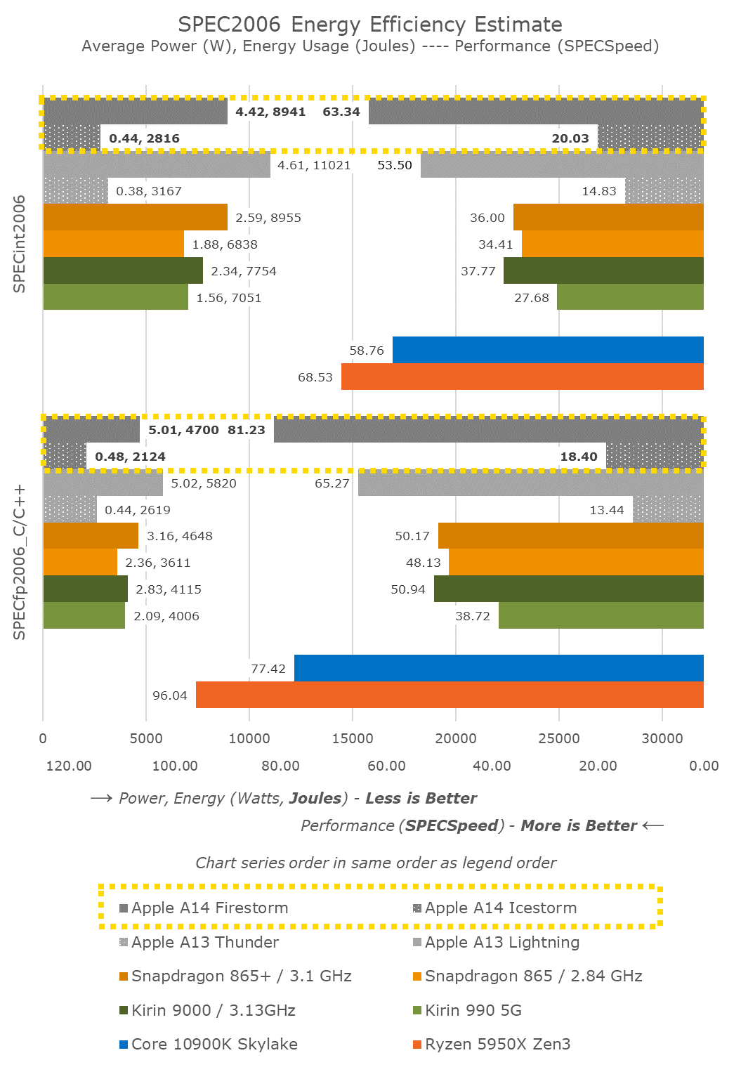
The process node is actually quite the wildcard in the comparisons here as the A14 is the first 5nm chipset on the market, closely followed by Huawei’s Kirin 9000 in the Mate 40 series. We happen to have both devices and chips in house for testing, and contrasting the Kirin 9000 (Cortex-A77 3.13GHz on N5) vs the Snapdragon 865+ (Cortex-A77 3.09GHz on N7P) we can somewhat deduct how much of an impact the process node has in terms of power and efficiency, translating those improvements to the A13 vs A14 comparison.

Starting off with SPECint2006, we don’t see anything very unusual about the A14 scores, save the great improvement in 456.hmmer. Actually, this wasn’t due to a microarchitectural jump, but rather due to new optimisations on the part of the new LLVM version in Xcode 12. It seems here that the compiler has employed a similar loop optimisation as found on GCC8 onwards. The A13 score actually had improved from 47.79 to 64.87, but I hadn’t run new numbers on the whole suite yet.
For the rest of the workloads, the A14 generally looks like a relatively linear progression from the A13 in terms of progression, accounting for the clock frequency increase from 2.66GHz to 3GHz. The overall IPC gains for the suite look to be around 5% which is a bit less than Apple’s prior generations, though with a larger than usual clock speed increase.
Power consumption for the new chip is actually in line, and sometimes even better than the A13, which means that workload energy efficiency this generation has seen a noticeable improvement even at the peak performance point.
Performance against the contemporary Android and Cortex-core powered SoCs looks to be quite lopsided in favour of Apple. The one thing that stands out the most are the memory-intensive, sparse memory characterised workloads such as 429.mcf and 471.omnetpp where the Apple design features well over twice the performance, even though all the chip is running similar mobile-grade LPDDR4X/LPDDR5 memory. In our microarchitectural investigations we’ve seen signs of “memory magic” on Apple’s designs, where we might believe they’re using some sort of pointer-chase prefetching mechanism.
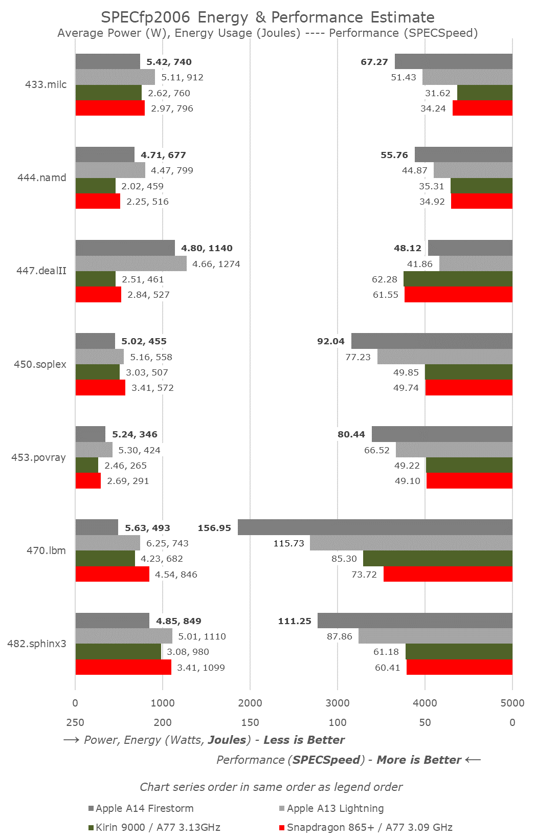
In SPECfp, the increases of the A14 over the A13 are a little higher than the linear clock frequency increase, as we’re measuring an overall 10-11% IPC uplift here. This isn’t too surprising given the additional fourth FP/SIMD pipeline of the design, whereas the integer side of the core has remained relatively unchanged compared to the A13.
In the overall mobile comparison, we can see that the new A14 has made robust progress in terms of increasing performance over the A13. Compared to the competition, Apple is well ahead of the pack – we’ll have to wait for next year’s Cortex-X1 devices to see the gap narrow again.
What’s also very important to note here is that Apple has achieved this all whilst remaining flat, or even lowering the power consumption of the new chip, notably reducing energy consumption for the same workloads.
Looking at the Kirin 9000 vs the Snapdragon 865+, we’re seeing a 10% reduction in power at relatively similar performance. Both chips use the same CPU IP, only differing in their process node and implementations. It seems Apple’s A14 here has been able to achieve better figures than just the process node improvement, which is expected given that it’s a new microarchitecture design as well.
One further note is the data of the A14’s small efficiency cores. This generation we saw a large microarchitectural boost on the part of these new cores which are now seeing 35% better performance versus last year’s A13 efficiency cores – all while further reducing energy consumption. I don’t know how the small cores will come into play on Apple’s “Apple Silicon” Mac designs, but they’re certainly still very performant and extremely efficient compared to other current contemporary Arm designs.
Lastly, there’s the x86 vs Apple performance comparison. Usually for iPhone reviews I comment on this in this section of the article, but given today’s context and the goals Apple has made for Apple Silicon, let’s investigate that into a whole dedicated section…


644 Comments
View All Comments
pcordes - Thursday, November 19, 2020 - link
Thanks for the microarchitectural testing and details!However, some current Intel / AMD numbers you use for comparison aren't right. (Also, your ROB-size and load/store buffers graphs are missing labels on the vertical axis; I assume that's time or cycles or something with.)
Intel since Skylake has 5-wide legacy decode (up from 4-wide in Haswell) and 6-wide fetch from the decoded-uop cache. (The issue/rename stage is still only 4-wide in Skylake, but widened to 5 in Ice Lake. Being wider earlier in the front-end can catch up after stalls, letting buffers between stages hide bubbles) https://en.wikichip.org/wiki/intel/microarchitectu...
https://en.wikichip.org/wiki/intel/microarchitectu...
(The decoders can also macro-fuse a cmp/jcc branch into 1 uop, so max decode throughput is actually 7 x86 instructions per clock, into 5 uops.)
AMD Zen 2 can decode up to 4 x86 instructions per clock. (Not sure if that includes fusion of cmp/jcc or not). This is probably where you got your 4-wide number that you claimed applied to Intel. But that's just legacy-decode. Most code spends a lot of time in non-huge loops, and they can run from the uop cache. Zen 2's decoded-uop cache can produce up to 8 uops/clock.
https://en.wikichip.org/wiki/amd/microarchitecture...
The actual bottleneck for sending instructions into the out-of-order back-end is the issue/rename stage as usual: 6 uops, but I think those can only come from up to 5 x86 instructions. I thought I remembered reading that Zen 1 could only sustain 6 uops / clock when running code that included some AVX 256-bit instructions or other 2-uop instructions. Maybe that changed with Zen2 (where most 256-bit SIMD instructions are still 1 uop), I don't have an AMD system to test on, and stuff like https://uops.info/ only tests throughput of single instructions, not a mix of integer, FP, and/or loads/store.
Anyway, Zen's front-end is at least 5-wide, and 6-wide for at least some purposes.
---
You seem to be saying M1 can do 4 FADDs *and* 4 FMULs in the same cycle. That doesn't make any sense with "only" 4 FP execution units. Perhaps you mean 4 FMAs per cycle? Or can each execution unit really accept 2 instructions in the same clock cycle, like Pentium 4's double-pumped integer ALUs?
That's only twice the throughput of Haswell/Skylake, or the same throughput if you take vector width into account, assuming Apple M1 doesn't have ARM SVE for wider vectors.
(Skylake has FMA units on ports 0 and 1, each 256-bit wide. FP mul / add also run on those same units, all with 4-cycle latency. So using FMAs instead of `vaddps` or `vmulps` gives Skylake twice the FLOPS because an FMA counts as two FLOPs, despite being a single operation for the pipeline.)
Zen2 runs vaddps on ports FP2 / FP3, and vmulps or vfma...ps on FP0 / FP1. So it can sustain 2/clock FADD *and* 2/clock FMUL/FMA, unlike Skylake that can only do a total of 2 FP ops per cycle. (Both with any width from scalar to 256-bit). Zen1 has the same port allocations, but the execution units are only 128 bits wide. (Numbers from https://uops.info/)
https://en.wikichip.org/wiki/amd/microarchitecture... doesn't indicate any more FMA or SIMD FP mul/add throughput, except reduced competition from FP store and FP->int.
You weren't looking at actual legacy x87 `fadd` / `fmul` instruction mnemonics were you? Modern x86 does FP math using SSE / AVX instructions like scalar addsd / mulsd (sd = scalar double), with fewer execution units for legacy 80-bit x87. (Unfortunately FMA isn't baseline, only available as an extension, unlike with AArch64.)
LYP - Sunday, May 23, 2021 - link
I'm happy that I'm not the only one who thinks there is something wrong here ...peevee - Wednesday, December 9, 2020 - link
"Intel has stagnated itself out of the market, and has lost a major customer today."A decade+ concentrating on "diversity and inclusion" vs competency can do that to you. Their biggest problem today might be the Portland location and culture.
IntoGraphics - Wednesday, December 16, 2020 - link
<blockquote>"If Apple’s performance trajectory continues at this pace, the x86 performance crown might never be regained."</blockquote>If Apple's performance trajectory does continue at this pace, the x86 performance crown will be irrelevant.