2021 NAND Flash Updates from ISSCC: The Leaning Towers of TLC and QLC
by Billy Tallis on February 19, 2021 10:00 AM EST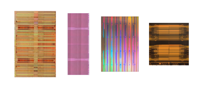
The annual IEEE International Solid-State Circuits Conference covers a range of topics of interest to AnandTech. Every year the conference includes a session on non-volatile memories where most of the NAND flash memory manufacturers share technical details of their latest developments. At the conference we get more information than these companies are usually willing to share in press briefings, and the presentations are usually about technology that will be hitting the market during the coming year.
At ISSCC 2021 this week, four of the six major 3D NAND flash memory manufacturers are presenting their newest 3D NAND technology. Samsung, SK hynix and Kioxia (+Western Digital) are sharing their latest 3D TLC NAND designs and Intel is presenting their 144-layer 3D QLC NAND. Not participating this year are Micron (who announced their 176L 3D NAND late last year) and Chinese newcomer YMTC.
3D TLC (3-bit per cell) Updates
Samsung, SK hynix, and Kioxia/WD presented information about their upcoming generations of 3D TLC. Not shown here is Micron's 176L TLC, because they haven't released most of this data for their latest generation of 3D NAND.
| 3D TLC NAND Flash Memory ISSCC Presentations |
||||||
| Samsung | SK hynix | Kioxia (Toshiba) WD |
||||
| Year Presented at ISSCC | 2021 | 2019 | 2021 | 2021 | 2019 | 2018 |
| Layers | 128 | 176 | >170 | 128 | 96 | |
| Die Capacity | 512 Gb | 512 Gb | 512 Gb | 1 Tb | 512 Gb | 512 Gb |
| Die Size (mm2) | 101.58 | 98 | 66 | 86 | ||
| Density (Gbit/mm2) | 8.5 | 5 | 10.8 | 10.4 | 7.8 | 5.95 |
| IO Speed | 2.0 Gb/s | 1.2 Gb/s | 1.6 Gb/s | 2.0 Gb/s | 1.066 Gb/s | 533 Mb/s |
| Program Throughput | 184 MB/s | 82 MB/s | 168 MB/s | 160 MB/s | 132 MB/s | 57 MB/s |
| Read Latency (tR) | 40 µs | 45 µs | 50 µs | 50 µs | 56 µs | 58 µs |
| Erase Block Size | 24 MB | 18 MB | ||||
| Planes | 4? | 2 | 4 | 4 | 4 | 2 |
| CuA / PuC | Yes | No | Yes | Yes | Yes | No |
Unsurprisingly, it looks likely that Samsung will again be in the lead for performance, with the lowest read latency and fastest write speeds. However, their bit density is still clearly lagging even though they're claiming a 70% jump with this generation. In the past, their lagging density hasn't been as much of a downside as it might appear at first glance, because Samsung has been able to avoid using string stacking and can manufacture a stack of 128 layers as a single deck while their competitors have all had to split their stack into two decks, increasing the number of fab steps required. This might be the generation that brings Samsung's inevitable adoption of string stacking, but if that's the case then their lingering density disadvantage is rather disappointing. On the other hand, if they've managed to put off that transition for one more generation and achieved this kind of density increase only using a combination of other techniques (most notably a CMOS under Array layout), then it's a very impressive advance and it would be safe to say that Samsung is years ahead of the competition when it comes to the high aspect ratio etching of the vertical channels that is the most critical fab step in scaling 3D NAND. We'll know more once Samsung discloses the actual layer count, but they're keeping that secret for now—which hints that they don't expect to have the highest layer count to brag about.
The TLC parts described by SK hynix and Kioxia/WD look fairly similar, save for the big difference that SK hynix is talking about a 512Gb die and Kioxia is talking about a 1Tb die. Both designs look to have similar performance and density, though Kioxia is touting a higher NAND interface speed. Kioxia and Western Digital have put out a press release announcing 162-layer 3D NAND, so they're a bit behind SK hynix and Micron for total layer count. That press release also mentions a 10% improvement in the horizontal density of their cell array, so Kioxia and Western Digital are probably packing the vertical channels closer together than any of their competitors.
3D QLC (4-bit per cell) Updates
The only company with updates this year on QLC is Intel.
| 3D QLC NAND Flash Memory ISSCC Presentations |
|||||||
| Intel | Samsung | SK hynix | Kioxia WD |
||||
| Year Presented at ISSCC | 2021 | 2020 | 2020 | 2018 | 2020 | 2019 | |
| Layers | 144 | 96 | 92 | 64 | 96 | 96 | |
| Die Capacity | 1 Tb | 1 Tb | 1 Tb | 1 Tb | 1 Tb | 1.33 Tb | |
| Die Size (mm2) | 74.0 | 114.6 | 136 | 182 | 122 | 158.4 | |
| Density (Gbit/mm2) | 13.8 | 8.9 | 7.53 | 5.63 | 8.4 | 8.5 | |
| IO Speed | 1.2 Gb/s | 800 Mb/s | 1.2 Gb/s | 1.0 Gb/s | 800 Mb/s | 800 Mb/s | |
| Program Throughput | 40 MB/s | 31.5 MB/s | 18 MB/s | 12 MB/s | 30 MB/s | 9.3 MB/s | |
| Program Latency (tPROG) | 1630 µs | 2080 µs | 2 ms | 3 ms | 2.15 ms | 3380 µs | |
| Read Latency (tR) |
Avg | 85 µs | 90 µs | 110 µs | 145 µs | 170 µs | 160 µs |
| Max | 128 µs | 168 µs | 165 µs | ||||
| Erase Block Size | 48 MB | 96 MB | 16 MB | 24 MB | 24 MB | ||
| Planes | 4 | 4 | 2 | 2 | 4 | 2 | |
In general, Intel has been more focused on QLC NAND than any of its competitors. This 144L QLC is the first generation of 3D NAND Intel hasn't co-developed with Micron, and it is unique in several respects. Intel is taking its 3D NAND technology in different directions from the rest of the industry will have interesting ramifications for their agreement to sell the NAND flash business to SK hynix, but in the short term it seems like Intel is getting the NAND they want to be selling. With only 144 layers, Intel is almost certainly now in the last place for total layer count. Compared to 9x-layer QLC, Intel has much better performance and density—but QLC versions of the new TLC described by SK hynix and Kioxia should have comparable density. Intel has backed off from the frankly astronomical erase block size their 96L QLC used, but the 48MB block size of their new 144L QLC still seems a bit high.
CMOS Under Array From Everyone
Intel and Micron's now-dissolved joint venture was the second NAND flash manufacturer to make the switch to 3D NAND, after Samsung. The most significant innovation the Intel/Micron 3D NAND brought to the industry was the CMOS Under the Array (CuA) design. This places most of the NAND die's peripheral circuitry—page buffers, sense amplifiers, charge pumps, etc.—under the vertical stack of memory cells instead of alongside.
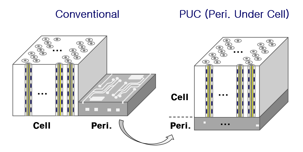
This change saves a big chunk of die space and allows for over 90% of the die area to be used for the memory cell array. SK hynix was next to make this switch, which they call "Periphery under Cell" (PuC). The rest of the manufacturers are now also onboard: Kioxia (then Toshiba) and Western Digital presented a 128-layer CuA design at ISSCC 2019 but their fifth generation BiCS 3D NAND ended up going into production as a 112L design without CuA. Their ISSCC presentation this year is for a "170+" layer design with CuA, and they've put out a press release confirming that their sixth generation BiCS 3D NAND will be a 162-layer design with CuA.
Aside from saving die space, a CuA/PuC style design for 3D NAND allows for a die to include more peripheral circuitry than would otherwise be cost-effective. This makes it practical to divide a die's memory array into more separate planes, each with their own copies of much of the peripheral circuitry. Most 3D NAND that has been built without a CuA layout has used just two planes per die, but now that everyone is using CuA the standard is four planes per die. This provides extra parallelism that increases the performance per die and offsets the overall SSD performance drop that usually comes from using fewer dies to reach the same total capacity.
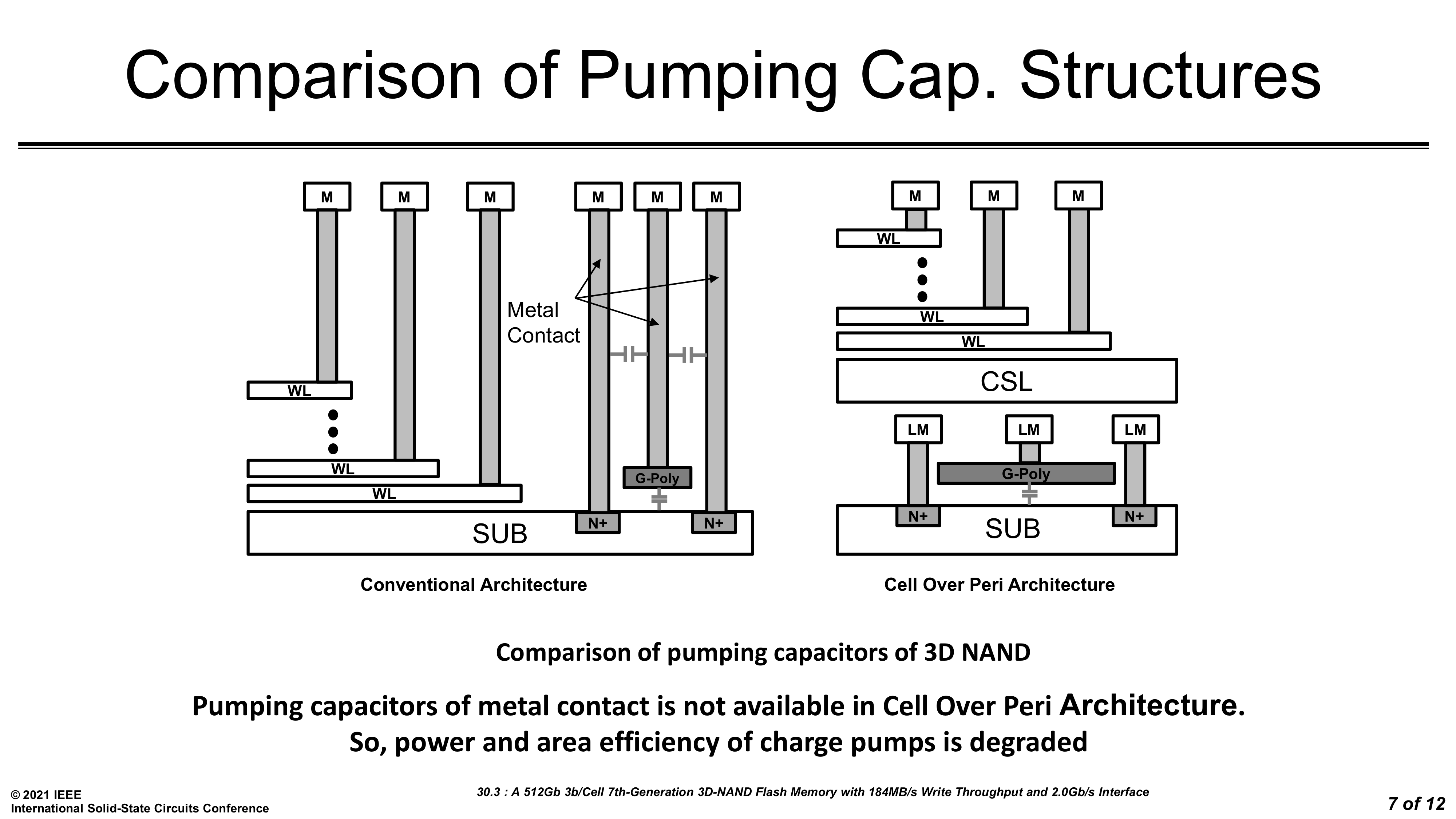
A CuA structure is not without its challenges and downsides. When a manufacturer first switches to CuA they get a big increase in available die space for peripheral circuitry. But after that, each successive generation that adds layers means there's less die space available for managing the same number of memory cells, so peripheral circuitry still has to shrink. Putting peripheral circuitry under the memory cell array also introduces new constraints. For example, Samsung's ISSCC presentation this year mentions the challenges of constructing large capacitors for the charge pumps when they can no longer use the tall metal structures that are simple to include alongside the 3D NAND stack.
Better On-Die Parallelism: Four Planes Per Die
Dividing a NAND flash die into four planes allows for the die to handle more operations in parallel, but doesn't make it behave quite like four independent dies. There are restrictions on what can be done in parallel: for example, simultaneous writes still have to go to the same word line within each plane. But as the number of planes in a flash die grows, manufacturers have been working to loosen some of those restrictions. In previous years, manufacturers have introduced *independent* multi-plane reads, meaning simultaneous reads in different planes don't have any restrictions on the locations within each plane that are being read—a big win for random read throughput.

Now, another restriction on multi-plane operations is being relaxed: the timing of read operations in different planes doesn't need to line up. This makes it possible for one plane to perform multiple reads from SLC pages while another plane is performing a single slower read from TLC or QLC pages. This capability is called Asynchronous Independent (Multi-)Plane Read. The practical effect is that for read operations, a large 4-plane die can now match the performance of four smaller 1-plane dies. This mitigates many of the performance downsides that higher per-die capacity brings to SSDs that only have one or two dies per channel.
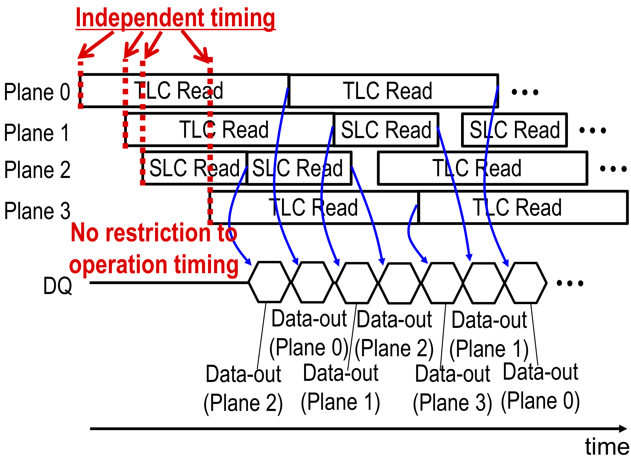
Kioxia and WD reported that implementing this capability required them to stop sharing charge pumps between planes, in order to avoid poorly-timed voltage and current fluctuations that would have resulted from unsynchronized read operations. Intel is also halfway to this capability with their 4-plane 144L QLC: planes are paired up into plane groups, and each plane group can perform reads without needing to align with the timing of reads in the other plane group.
NAND IO Speeds Outpacing SSD Controller Support
The new TLC NAND parts described at ISSCC support IO speeds ranging from 1.6 to 2.0 Gb/s for communication between the NAND flash dies and the SSD controller. The fastest NAND in SSDs currently on the market runs at 1.2-1.4Gb/s. The NAND manufacturers can benefit from vertical integration by ensuring that their own SSD controller designs used for their own SSDs will be ready to support these higher IO speeds, but other SSD vendors that rely on third-party controllers may be left behind. Phison's latest E18 8-channel controller for high-end PCIe 4.0 SSDs only supports 1.2Gb/s IO speeds, and their upcoming E21T 4-channel NVMe controller supports 1.6Gb/s. Silicon Motion's 8-channel SM2264 and 4-channel SM2267 support 1.6Gb/s and 1.2Gb/s IO speeds respectively.
Since 8 channels running at 1.2Gb/s is already enough for a SSD to saturate a PCIe 4.0 x4 connection, these new higher IO speeds will not be of much use to high-end SSDs until PCIe 5.0 arrives. But more affordable 4-channel consumer SSD controllers will be able to use these higher speeds to move up well into PCIe 4.0 performance territory, matching or exceeding the throughput that the first PCIe 4.0 SSD controller (Phison E16, 8ch @ 800Mb/s) offered. As demonstrated by drives like the SK hynix Gold P31, an advanced 4-channel controller supporting high IO speeds on each channel can be very competitive on performance while operating with far higher power efficiency than 8-channel controllers.
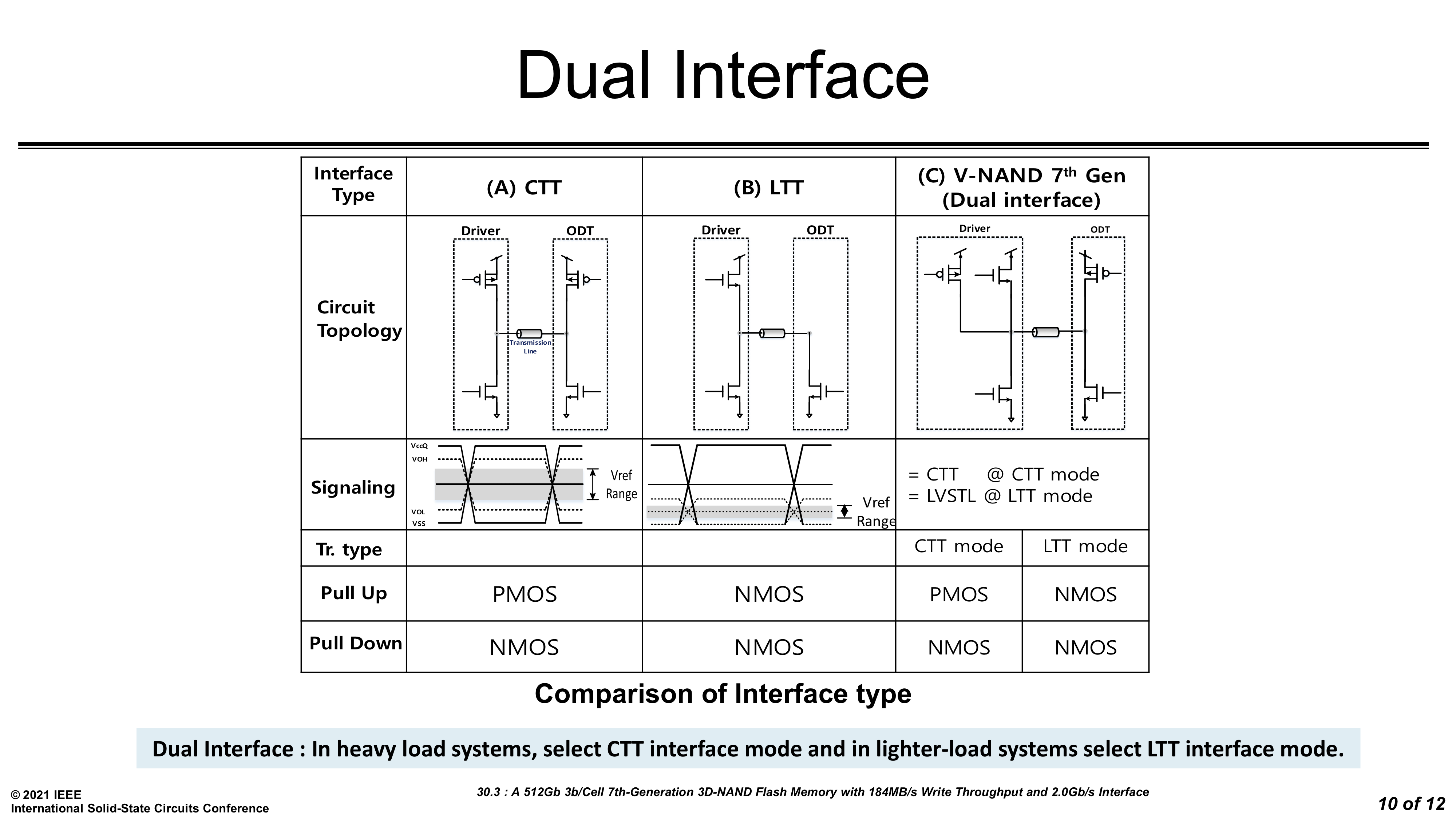
Hitting these higher IO speeds requires major upgrades to the interface logic on the NAND dies, and as we've seen with other high-speed interfaces like PCI Express, increasing power consumption is a major concern. Samsung is addressing this by using dual-mode drivers and termination. When higher drive strength is needed because of more load on the bus (from more dies per channel), the'll use a PMOS transistor for pull-up, and otherwise they can use a NMOS transistor and cut the power consumption of the driver by more than half. This gives Samsung a single interface design that will work well for both small consumer SSDs and large enterprise drives with many more dies per channel. (In the past Samsung has added separate retimer dies to multi-chip packages that stack lots of NAND dies together on the same one or two channels. We're not sure if Samsung is still using this technique.)
String Stacking: First Triple-Deck NAND
String stacking has been viewed as something of a necessary evil for scaling up 3D NAND to higher layer counts. Only Samsung has managed to build more than 100 layers of 3D NAND at a time, and everyone else has long since switched to stacking two decks each with a more reasonable layer count. This means that eg. Micron's 176-layer 3D NAND is built as 88 layers of memory cells, then another 88 layers are constructed on top. This drives up cost compared to doing all the layers at once, and it requires careful alignment at the interface between decks. But the alternative would be to make the vertical channels much wider, so that the aspect ratio (width vs depth) would stay within the realm of what can be feasibly etched by current fab techniques.
Intel's 144L QLC design includes the surprise that they are already moving to a 3-deck stack: 48+48+48 layers rather than the 72+72 we would expect. Since their previous generation is a 48+48 layer (96L total) design, it's possible that they have changed very little about how the memory array itself is fabricated aside from repeating the same sequence of deposition, etch and fill steps a third time. Intel is taking a hit on fab throughput with this approach, but it probably helps them better control the variation in channel and cell dimensions from the top to bottom of the stack, which may be more of a concern given their focus on QLC and their unique decision to still use a floating gate memory cell rather than switching to a charge trap cell like everyone else.
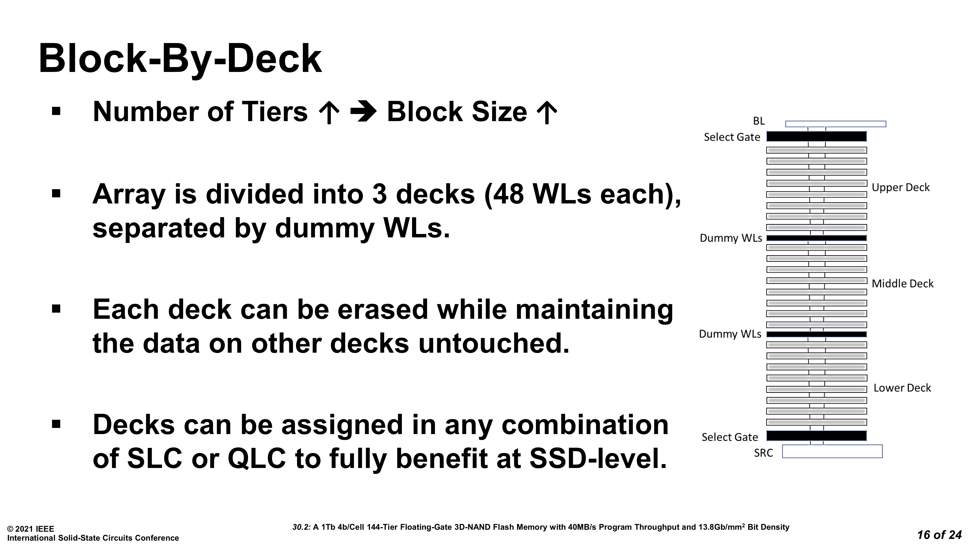
To go along with this triple-deck structure, Intel has reorganized how they handle erase blocks, and now each of the three decks constitutes a separate collection of erase blocks. That means the middle third of a 144L string can now be erased without interfering with the data stored in the other two thirds of the string. Dividing blocks by decks is also how Intel was able to reduce the 96 MB block size with their 96L QLC down to a less extreme 48MB block size.
A Small Caveat about Academic Conferences
It's important to understand that ISSCC, where these updates are presented, is an academic conference. The presentations are not product announcements and the papers are not product spec sheets. The designs presented at ISSCC don't always match what goes into mass production. For example, Kioxia/WD in the past have presented designs for 128L and "170+" layer NAND, but their actual fifth and sixth generation BiCS NAND as mass produced are 112L and 162L designs. They also, despite mentioning it in their 2019 talk, deferred a switch to a more dense 'CMOS under Array (CuA) structure' to a later product line. Specifications such as write performance are also often presented as best-case, and real world products end up being a notch below what is presented.
Despite the coming together of all these companies under one conference, even when the presentation does match the eventual product, what we learn from ISSCC is usually imperfect and incomplete information. The companies are inconsistent about what metrics they report, and we usually get information for only one die design per generation—a company might present their 512Gbit design even if they're planning to manufacture both 512Gbit and 256Gbit parts. In recent years several companies seem to be alternating between talking about their QLC one year and TLC the next. In spite of all of that, ISSCC presentations on 3D NAND are still a great way to gauge how the state of the art has progressed and where the industry as a whole is headed.
About half the content of these presentations is clever schemes for micromanaging voltages applied to various wires to optimize the read, program and erase processes. There are complex tradeoffs between speed, accuracy, wear and other factors. we're not going to dig into all of these details, other than to say that programming a cell to the desired voltage (and without disturbing other cells) is not a simple process, and even reading from a TLC or QLC cell is quite a bit more complicated than reading from a DRAM or SRAM cell. We're more interested in any major structural changes in the dies themselves, and the end results of all the finessing of voltages: the speeds at which a page of memory can be read or programmed.


75 Comments
View All Comments
GeoffreyA - Wednesday, February 24, 2021 - link
Concerning quantum computers, I need to get a better grip on the topic. I remember when first reading about them in 2016, I felt a bit sceptical, especially concerning that DWAVE machine or whatever it was called. But, need to bring myself up to date on the topic."if you somehow manage to live long enough, you'll freeze. The universe will ultimately undergo heat death"
I think one can spend a lifetime meditating on this topic, about the end of the universe, heat death, and entropy. I used to think about it a lot but haven't in a while, so it's hazy. (Still have to work out whether Nolan's reverse entropy was nonsense or plausible.) Anyway, there's some elusive link between time, entropy, heat, and the cooling at the end. Tegmark had some nice remarks there, as well as Penrose and Rovelli. As to fiction, Asimov's "Last Question" is well worth reading if you haven't already. It's about a computer that ponders the question: how can the heat death be avoided, and entropy reversed? The ending is golden. I apologise for the poor link but couldn't find a better one:
baencd.freedoors.org/Books/The%20World%20Turned%20Upside%20Down/0743498747__19.htm
GeoffreyA - Wednesday, February 24, 2021 - link
"Until then, I just see it as a marvel of human understanding that's beautiful in its weirdness and otherness."It's mind-boggling how the human mind found out all these things. Even our devices today spring from these discoveries. I doubt whether physics will be solved in our lifetime. Yet, I just wish I could understand "why," and what's out there, beyond our universe. Some will say a futile question but I think about it often.
GeoffreyA - Wednesday, February 24, 2021 - link
https://novels80.com/the-complete-stories/the-last...mode_13h - Thursday, February 25, 2021 - link
Thanks for the recommendation. I'll check it out, sometime.mode_13h - Monday, February 22, 2021 - link
> Inside a SSD, the SSD firmware deals with the minutiae, not the OS.There's a move to expose the details of SSDs for the host to manage, rather than the SSD controller having to guess what the host OS/application wants. It's mostly for enterprise applications, though. I forget what name it's under.
> As for the CPU, the CPU firmware deals with the caches, not the OS.
That's not true. Even leaving aside security mitigations, software (i.e. OS/drivers) always had to flush or invalidate caches for memory regions being read/written by devices.
> You may be thinking that's a lot of black boxes. It makes for flexible software and hardware, where different parts can be swapped for improved versions without the rest of the system needing to know that anything has changed.
This is a convenient approach, until either the cost of those abstractions adds up, or they prevent software from doing clever optimizations that can't be anticipated by the caches. For instance, GPUs have at least some of the on-chip memories managed by the software, because it has a better idea of what data it wants fast access to, and for how long. Also, caching has overheads, even when it does exactly what you want.
Spunjji - Monday, February 22, 2021 - link
That would be ZNS:https://www.anandtech.com/show/15959/nvme-zoned-na...
GeoffreyA - Monday, February 22, 2021 - link
"the cost of those abstractions adds up"Indeed, that's why there's been the trend of late to go closer to the hardware, like DirectX 12, Vulkan, and Metal.
FunBunny2 - Thursday, February 25, 2021 - link
"there's been the trend of late to go closer to the hardware"as a wise guy I used to know (Ph.D. in math stat) said, "infinite granularity yields infinite complexity".
mode_13h - Thursday, February 25, 2021 - link
The trick is to have an API that hides enough details that you get portability between different hardware (and that includes running *well* on them, sometimes referred to as "performance portability"), while still being as easy as possible to use (correctly) and low-overhead enough that it doesn't hamper the perfomance and lead to developers seeking other options.That's not a small order, and goes some ways towards explaining why APIs need to change with the technology (both on host and device-side). Also, workloads evolve with the technology, and that exposes new bottlenecks or limits on the scalability of earlier APIs.
GeoffreyA - Saturday, February 27, 2021 - link
I agree, that's the ideal. Many APIs and frameworks were taken a bit too far, where ease, tidiness, and security came before everything else. Over time, or from the word go, their performance was lacking. Though I haven't used it, Microsoft's .NET comes to mind; and Qt, while being fun, tends to encourage one to use features in an inefficient way.Certainly no expert but I'd say the Win32 API is an example of having the right balance. It forces programmers to work in a roundabout but efficient way, compared to newer frameworks and languages, where the shorter styles tend to come at a cost. Sure, it's old-fashioned and clumsy, but has a strange elegance.