Intel Rocket Lake (14nm) Review: Core i9-11900K, Core i7-11700K, and Core i5-11600K
by Dr. Ian Cutress on March 30, 2021 10:03 AM EST- Posted in
- CPUs
- Intel
- LGA1200
- 11th Gen
- Rocket Lake
- Z590
- B560
- Core i9-11900K
A Rocket Lake Retrofit: 10nm onto 14nm
The new generation Rocket Lake processor family is the combination of two different backported technologies. Intel took the Sunny Cove core from its 10nm Ice Lake processor, and re-built it on 14nm, calling it now Cypress Cove. Intel also took the Xe graphics from 10nm Tiger Lake and re-built those on 14nm, but these are still called Xe graphics, albeit labelled UHD 750.
We can see that the new design is an amalgam of new technologies, by comparing Rocket Lake to Comet Lake, Ice Lake, and Tiger Lake:
| Microarchitecture Comparison | |||||
| AnandTech | Comet Lake |
Rocket Lake |
Ice Lake |
Tiger Lake |
Ryzen 5000 |
| Form Factor | Desktop | Desktop | Laptop | Laptop | Desktop |
| Max Cores | 10 | 8 | 4 | 4 | 16 |
| TDP | 125 W | 125 W | 28 W | 35 W | 105 W |
| uArch | Comet | Cypress | Sunny | Willow | Zen 3 |
| IGP | Gen 9 | Xe-LP | Gen 11 | Xe | - |
| IGP Cores | 24 | 32 | 64 | 96 | - |
| L1-D | 32 KB /c | 48 KB /c | 48 KB /c | 48 KB/c | 32 KB/c |
| L2 Cache | 256 KB /c | 512 KB /c | 512 KB/c | 1280KB /c | 512 KB/c |
| L3 Cache | 20 MB | 16 MB | 8 MB | 12 MB | 64 MB |
| PCIe | 3.0 x16 | 4.0 x20 | 3.0 x8 | 4.0 x4 | 4.0 x24 |
| DDR4 | 2 x 2933 | 2 x 3200 | 2 x 3200 | 2 x 3200 | 2 x 3200 |
| LPDDR4X | - | - | 4 x 3733 | 4 x 4266 | - |
There are obviously some differences between the notebook and desktop parts, most noticeably that the new platform at the high-end has only eight cores, two fewer than Comet Lake.
Additional improvements over Comet Lake include AVX512 units, support for 20 PCIe 4.0 lanes, and faster memory. With the new chipsets, Intel has already disclosed that the Rocket Lake platform will have native USB 3.2 Gen 2x2 (20 Gbps), and with the Z590 motherboards, a double bandwidth link from CPU to the chipset, moving from DMI x4 to DMI x8, effectively a PCIe 3.0 x8 link.
Rocket Lake on 14nm: The Best of a Bad Situation
The delays around the viability of Intel’s 10nm manufacturing have been well documented. To date, the company has launched several products on its 10nm process for notebooks, such as Cannon Lake, Ice Lake, Jasper Lake, Elkhart Lake, and Tiger Lake. There have been other non-consumer products, such as Agilex FPGAs and Snow Ridge 5G SoCs, and Intel has confirmed that its 10nm server products ‘Ice Lake Xeon Scalable’, are currently in volume production for an early Q2 launch on April 6th.
The one product line missing from that list is the desktop and enthusiast segments that typically use socketed processors paired with discrete graphics. Intel has always committed to launching desktop processors on its 10nm process, however we are yet to see the results of their efforts. The issues Intel is having with 10nm have not been fully disclosed at this time, with Intel instead happy to promote some of the improvements made, such as its new SuperFin technology, which is in Tiger Lake and the next-generation server platform beyond Ice Lake Xeon Scalable (for those keeping track, that would be Sapphire Rapids). The 10nm improvements so far has enabled Intel to launch notebook processors and server processors, both of which have lower power-per-core than a typical desktop offering.
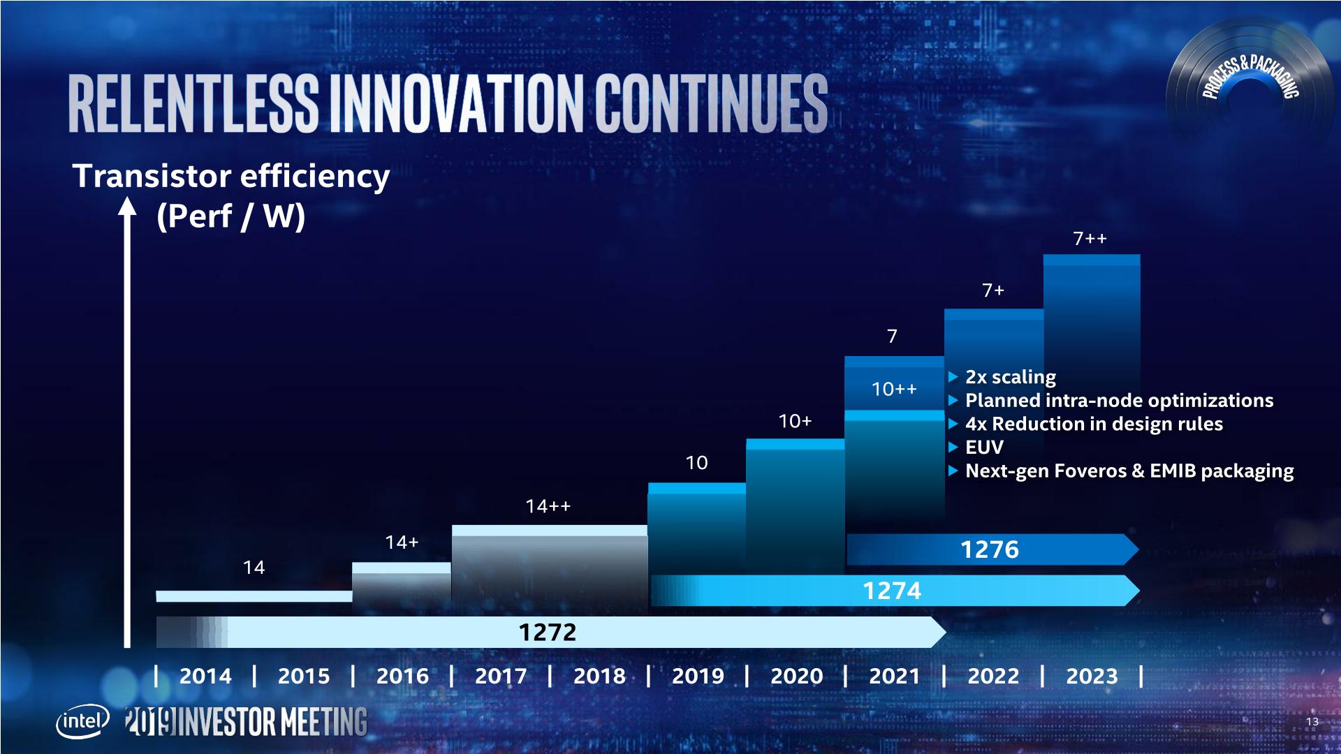
As 10nm has not been able to meet the standards required for desktop-level performance, rather than leave a potential 3 year gap in the desktop product family, Intel has been in a holding pattern releasing slightly upgraded versions of Skylake on slightly improved variants of 14nm. The first two members of the Skylake family, Skylake and Kaby Lake were released as expected. While waiting, we saw Intel release Coffee Lake, Coffee Lake Refresh, and Comet Lake. Each of these afforded minor updates in frequency, or core count, or power, but very little in the way of fundamental microarchitectural improvement. The goal all along was to move to 10nm with the same architecture as the mobile Ice Lake processors, but that wasn’t feasible due to manufacturing limitations limiting how well the processors scaled to desktop level power.
- Skylake, Core 6th Gen in August 2015
- Kaby Lake, Core 7th Gen in January 2017 (+17mo)
- Coffee Lake, Core 8th Gen in October 2017 (+9mo)
- Coffee Lake Refresh, Core 9th Gen in October 2018 (+12mo)
- Comet Lake, Core 10th Gen in April 2020 (+18mo)
- Rocket Lake, Core 11th Gen in March 2021 (+11mo)
With each generation, Intel traditionally has either upgraded the process node technology, or updated the microarchitecture – a process that Intel called Tick-Tock. Originally Intel was set to perform a normal ‘Tick’ after Kaby Lake, and have Cannon Lake with the same effective Skylake microarchitecture move to 10nm. Cannon Lake ending up only as a laptop processor with no working graphics in a small number of notebooks in China as it was a hot mess (as shown in our review). As a result, Intel refocused its 10nm for notebook processors hoping that advances would also be applicable to desktop, but the company had to release minor upgrades on desktop from Coffee Lake onwards to keep the product line going.
This meant that at some level Intel knew that it would have to combine both a new architecture and a new process node jump into one product cycle. At some point however, Intel realized that the intercept point with having a new microarchitecture and the jump for the desktop to 10nm was very blurry, and somewhat intangible, and at a time when its main competitor was starting to make noise about a new product that could reach parity in single core performance. In order to keep these important product lines going, drastic measures would have to be taken.
After many meetings with many biscuits, we presume, the decision was made that Intel would take the core microarchitecture design from 10nm Ice Lake, which couldn’t reach high enough frequencies under desktop power, and repackage that design for the more dependable 14nm node which could reach the required absolute performance numbers. This is known as a ‘backport’.
Sunny Cove becomes Cypress Cove
The new Core 11th Gen processor which we are looking at today has the codename Rocket Lake. That’s the name for the whole processor, which consists of cores, graphics, interconnect, and other different accelerators and IP blocks, each of which also have their own codenames, just for the sake of making it easier for the engineers to understand what parts are in use. We use these codenames a lot, and the one to focus on here is the CPU core.
Intel’s 10nm Ice Lake notebook processor family uses Sunny Cove cores in the design. It is these cores that have been backported to 14nm for use in the Rocket Lake processors, and because it is on a different process node and there are some minor design changes, Intel calls them Cypress Cove cores.
The reason behind this is because taking a design for one manufacturing process and designing it for a second is no easy task, especially if it’s a regressive step – transistors are bigger, which means logic blocks are bigger, and all the work done with respect to signaling and data paths in the silicon has to be redone. Even with a rework, signal integrity needs to be upgraded for longer distances, or additional path delays and buffers need to be implemented. Any which way you cut it, a 10nm core is bigger when designed for 14nm, consumes more power, and has the potential to be fundamentally slower at execution level.
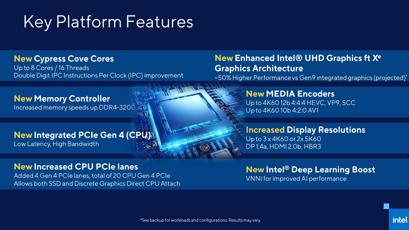
Intel’s official disclosures to date on the new Cypress Cove cores and Rocket Lake stem from a general briefing back in October, as well as a more product oriented announcement at CES in January. Intel is promoting that the new Cypress Cove core offers ‘up to a +19%’ instruction per clock (IPC) generational improvement over the cores used in Comet Lake, which are higher frequency variants of Skylake from 2015. However, the underlying microarchitecture is promoted as being identical to Ice Lake for mobile processors, such as caches and execution, and overall the new Rocket Lake SoC has a number of other generational improvements new to Intel’s desktop processors.
Eight Cores, Not Ten?
Enabling core designs through this backporting process is more complex than simply photocopying the design into the larger format. With every process node improvement, different density scalers and features are used in that process node that might not be available elsewhere. Undoubtedly the original 10nm Sunny Cove design had these in mind, and so having to re-architect the same floorplan with 14nm requires a lot of extra work. This adds transistors and buffers and ways to manage voltage differences and signal integrity in itself, increasing die size.
Note that Intel has in the past said that its 10nm process node offers a 2.7x transistor density increase moving from 14nm to 10nm. Naturally doing the reverse with a design, going from 10nm to 14nm, hasn’t made the core suddenly 270% bigger, namely because those numbers often refer to the densest transistors, and a high-performance microprocessor core often uses less dense transistors in logic to enable high-frequency with enough inactive silicon (dark silicon) to assist with power and thermals. We are still waiting on official numbers for core sizes, so it will be an interesting comparison between Sunny Cove and Cypress Cove.
Nonetheless, there is a core size increase, and this has to be factored into what silicon is produced. Designing a mass-production silicon layout requires balancing overall die size with expected yields, expected retail costs, required profit margins, and final product performance. Intel could easily make a 20+ core processor with these Cypress Cove cores, however the die size would be too large to be economical, and perhaps the power consumption when all the cores are loaded would necessitate a severe reduction in frequency to keep the power under control. To that end, Intel finalised its design on eight cores.
For die sizes, even with enabling only eight cores, the new Rocket Lake design is substantially bigger than the 10-core variant on Comet Lake.
| Intel Consumer Die Size Comparison All on Intel 14nm |
||||
| AnandTech | uArch | Cores | Die Size | |
| Core i7-8700K | Coffee Lake | 6 C | 9.2 x 16.7 mm | 153.6 mm2 |
| Core i9-9900K | CFL Refresh | 8 C | 9.2 x 19.6 mm | 180.3 mm2 |
| Core i9-10900K | Comet Lake | 10 C | 9.2 x 22.4 mm | 206.1 mm2 |
| Core i9-11900K | Rocket Lake | 8 C | 11.5 x 24.0 mm | 276.0 mm2 |
| HEDT for Comparison | ||||
| Core i9-7900X | Skylake-X | 10 C | 14.6 x 22.3 mm | 325.4 mm2 |
| Core i7-6950X | Broadwell-E | 10 C | 246.3 mm2 | |
So it's worth noting that Intel's new 8 core Rocket Lake processor is actually bigger than the 10 core Broadwell-E processor from 2016. One major difference between those two however is AVX-512, which does have a slight die-size increase. Nonetheless, Intel is approaching its HEDT platform die size with Rocket Lake, but can't sell them for as much as the HEDT has historically sold for. The Core i7-6950X sold for $1723, while the Core i7-7900X was $999. Intel's bulk of interest with this silicon is going to be the Core i7-11700K, which is a $420 processor.
Backport vs Co-Design
One of the critical elements to Rocket Lake is what it means for Intel going forward. With this project, Intel has taken a core designed for 10 nm and recreated the performance on 14 nm, with additional implications for power and efficiency. Intel has stated that in the future it will have cores designed for multiple process nodes at the same time, and so given Rocket Lake’s efficiency at the high frequencies, doesn’t this mean the experiment has failed?
I say no, because it teaches Intel a lot in how it designs its silicon. The issue with Rocket Lake is that the core was originally designed for 10 nm, and that won’t necessarily happen again.
Future cores from Intel are going to be designed, from the ground-up, for multiple process node technologies. Given Intel’s announcements about developing cores on external Intel manufacturing facilities, as well as licensing out its core designs, this means Intel might have to design a core that works at both Intel and TSMC. The point is that if Intel is going to do this, it will design for both from the start. The core will have been built taking into account the different elements of the process nodes in advance, and likely cater for the intricacies of both.
Rocket Lake by contrast, was an ‘after the fact’ redesign, with all of its special features built for 10 nm and then retrofit to 14 nm. Rocket Lake shows it can be done, but the way Intel went about this is unlikely to happen in the future. All future cores that require multiple process nodes, even across multiple foundry partners, are going to be co-designed from day one.
Ultimately, the future of how and when Intel will initiate additional co-design, even given suggested roadmaps, is likely to be in flux based on Intel’s own ability to produce high single-core frequency desktop processors. Cypress Cove, by most measures, is a reflex response to a widening gap in Intel’s desktop roadmap, and takes a core specifically designed for a different process. Intel is/has/has likely learned a lot from this process, but in the future we can expect specific cores to be co-designed with both process nodes in mind. This is akin to Intel’s new stance on ‘enabling the right product on the right node at the right time’. A co-designed approach, rather than a post-production realisation a backport is required, will mean that future core designs that straddle two process nodes are likely to be more similar and optimized on both processes at the same time.


279 Comments
View All Comments
Beaver M. - Wednesday, March 31, 2021 - link
Acting like GN and HUB gives them lots of AMD fanboy clicks/views.Beaver M. - Wednesday, March 31, 2021 - link
I guess living in isolation for a year makes people more and more antisocial and aggressive. And that then in turn sells well.Qasar - Wednesday, March 31, 2021 - link
so they are amd fanboys cause they told the truth ? more like you are the intel fanboy trying to defend this dud of a cpu. come on, most reviews say they same thing, just some are more harsh, and rightfully soOxford Guy - Wednesday, March 31, 2021 - link
Tech fans are continually disappointed by the lack of adequate competition in a multitude of tech markets (e.g. GPUs, CPUs, search, leading-edge lithography machines/foundries, etc. etc.)We saw, way back in the 80s, what happens when competition is shut down. The Japanese seized the DRAM market by dumping, forcing American DRAM makers out of the market — then promptly raising prices drastically.
We went from seeing revolutionary products like the Apple Lisa being replaced by years of toy-grade machines at very high prices. The Lisa shipped with 1 MB of RAM and the first Mac with just 128K. The Apple IIGS shipped with just 256K, many years after the Lisa. We can thank more than Apple's love of fat margins. We can thank inadequate competition.
We have seen that play out, time and time again. Now, it's so bad that it's worse than the bread lines of the USSR. At least if one waited in one of those one might end up with some bread. These days, you have two choices: a line to get a very overpriced product (like the latest iPhone) or you can skip waiting in line because they're nothing to buy (GPUs).
Oxford Guy - Wednesday, March 31, 2021 - link
(The Amiga 1000 only shipped with 256K of RAM, too, as I recall. It was a problem throughout the industry, not something due merely to Apple's margins.)GeoffreyA - Saturday, April 3, 2021 - link
I agree with your anti-corporation sentiment, but there's little we can do, except sigh. A worldwide boycotting of their products will work wonders but that'll never happen. As long as these rotters are out to make money---Intel, AMD, Google, the rest---it'll go on like this. Who knows, perhaps there's some vital link to entropy in all this, and why everything always goes awry on earth.Oxford Guy - Wednesday, March 31, 2021 - link
'One of the few tech sites that remained professional and didn't use click baity titles or disrespect intel.'This article uses bad spin to try to make Intel's product look better than it is.
Just one example:
‘Intel has stated that in the future it will have cores designed for multiple process nodes at the same time, and so given Rocket Lake’s efficiency at the high frequencies, doesn’t this mean the experiment has failed? I say no, because it teaches Intel a lot in how it designs its silicon’
The spin also includes the testing, using a really loud high-CFM CPU cooler in the Intel and a different quieter one on the AMD.
It's a pile of spin, like the glorified press release stuff trying to turn CEO Pat into some sort of superhero. That stuff sounds like it was written for investors.
FirstStrike - Wednesday, March 31, 2021 - link
Ian, you are missing SpecInt and SpectFp suiteOrkiton - Wednesday, March 31, 2021 - link
I'm not either Intel or AMD "fanboy" though some sympathy to AMD due to unfair, anti-competitive Intel practices in the past and AMD merit to emerge from their ashes. That said, best wishes to both in the name of progress, innovation and better value to us, the consumers.Oxford Guy - Wednesday, March 31, 2021 - link
The rated TDP is 125 W, although we saw 160 W during a regular load, 225 W peaks with an AVX2 rendering load, and 292 W peak power with an AVX-512 compute load.‘Intel’s claimed TDP’ rather than ‘that rated’. The latter implies an independent rating standard/body.
If both processors were found at these prices, then the comparison is a good one – the Ryzen 7 5800X in our testing scored +8% in CPU tests and +1% in gaming tests (1080p Max). The Ryzen is very much the more power-efficient processor, however the Intel has integrated graphics (an argument that disappears with KF at $374).
Again, no specifics about the power consumption difference.
On high-end gaming both processor performed the same, the AMD processor was ahead an average of 8% on CPU workloads, and the AMD processor came across as a lot more efficient and easy to cool, while the Intel processor scored a big lead in AVX-512 workloads.
Again, no specifics about the power consumption difference.
AGAIN, testing AMD with a weaker cooler, even though the CPU will go faster with the loud fast cooling you’re using on Intel.
Makes it APPLES to APPLES.