Intel Architecture Day 2021: Alder Lake, Golden Cove, and Gracemont Detailed
by Dr. Ian Cutress & Andrei Frumusanu on August 19, 2021 9:00 AM ESTGolden Cove Microarchitecture (P-Core) Examined
Section by Andrei Frumusanu
Within Alder Lake and Sapphire Rapids, we find Intel’s brand-new performance core (P-Core) microarchitecture, called Golden Cove. The new microarchitecture and core design follows the Willow Cove core in Tiger Lake, the Sunny Cove core in Ice Lake, and the derivative Cypress Cove core in Rocket Lake.
Although the new design is a follow-up over the last few years of core microarchitectures, Intel sees the Golden Gove as a major step-function update, with massive revamps of the fundamental building blocks of the CPU, going as far as calling it as allowing performance for the next decade of compute, meaning Intel is seemingly planning on using it as the basis for the evolution of cores for at least a few years.
The last time we had seen major upgrades to Intel’s core front-end was in Ice Lake's Sunny Cove, making notable increases in the microarchitecture’s out-of-order execution capabilities and depth, while Willow Cove and Cypress Cove were more iterative designs focusing on the memory subsystem.
Golden Cove, in comparison, makes gigantic changes to the microarchitecture’s front-end – in fact, Intel states that this is the largest microarchitectural upgrade in the core family in a decade, mirroring similar changes in magnitude to what Skylake had done many years ago.
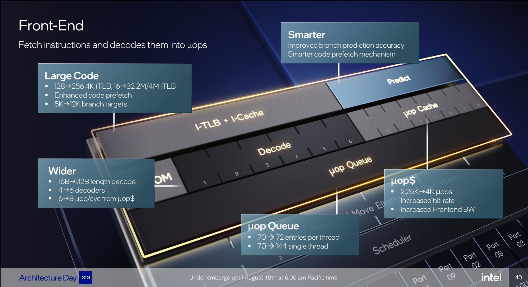
Starting off with the directly most obvious change: Intel is moving from being a 4-wide decode machine to being a 6-wide microarchitecture, a first amongst x86 designs, and a major design focus point. Over the last few years there had been a discussion point about decoder widths and the nature of x86’s variable length instruction set, making it difficult to design decoders that would go wider, compared to say a fixed instruction set ISA like Arm’s, where adding decoders is relatively easier to do. Notably last year AMD’s Mike Clarke had noted while it’s not a fundamental limitation, going for decoders larger than 4 instructions can create practical drawbacks, as the added complexity, and most importantly, added pipeline stages. For Golden Cove, Intel has decided to push forward with these changes, and a compromise that had to be made is that the design now adds an additional stage to the mispredict penalty of the microarchitecture, so the best-case would go up from 16 cycles to 17 cycles. We asked if there was still a kind of special-case decoder layout as in previous generations (such as the 1 complex + 3 simple decoder setup), however the company wouldn’t dwell deeper into the details at this point in time. To feed the decoder, the fetch bandwidth going into it has been doubled from 16 bytes per cycle to 32 bytes per cycle.
Intel states that the decoder is clock-gated 80% of the time, instead relying on the µOP cache. This has also seen extremely large changes this generation: first of all, the structure has now almost doubled from 2.25K entries to 4K entries, mimicking a similar large increase we had seen with the move from AMD’s Zen to Zen2, increasing the hit-rate and further avoiding going the route of the more costly decoders.
Although the I-cache has remained the same in terms of size at 32KB, Intel has improved latencies for larger code coverage by increasing the L1 iTLB from 128 entries to 256 entries (16 -> 32 for 2M/4M hugepages).
Because the general misprediction penalty has gone up this generation, Intel is very much counter-acting this by massively improving branch prediction accuracy. First of all, the L2 BTB (branch target buffer) has grown to well over double with the structure increased from 5K entries to 12K entries, making this by far the biggest in the industry that we’re aware of (Zen3: 6.5K, Cortex-A77+: 8K, Apple: ?). It is also said that the branch predictors themselves are now smarter, with their accuracy being improved, although these are always quite a bit secretive in terms of their designs so we didn’t have too many details divulged.
The decoders and the µOP cache feed a µOP queue – beyond he 50% larger decoder width, the µOP cache also now sees an increased bandwidth and able to emit 8 µOPs instead of 6. The µOP queue itself has seen a structural change, for single threads (only one SMT logical core is loaded), the structure can be aggregated and the usable depth has doubled from 70 entries to 144 entries, while for dual threads, has gone up slightly from 70 to 72 entries per thread.
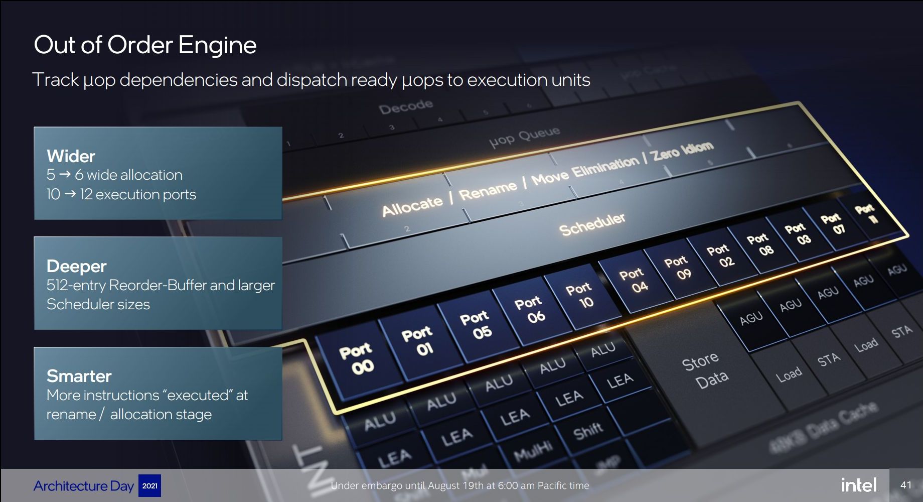
In the mid-core, there’s also been quite large changes. The core here increases from 5-wide to 6-wide, meaning that in theory it should still be a maximum 6 IPC microarchitecture, though we’re talking about µOPs here and not actual instructions.
Intel is noting that they’re doing an increased amount of dependency resolution at the allocation stage, actually eliminating instructions that otherwise would have to actually emitted to the back-end execution resources. Intel here didn’t want to elaborate a lot, only stating that this capability has increased quite a lot generation over generation.
The out-of-order instruction window of Golden Cove is massively larger than Sunny Cove – increasing the re-order buffer (ROB) size from 352 to 512 entries. This is over double that of AMD’s Zen3 µarch, and really only second to Apple’s core microarchitecture which we’ve measured in at around 630 instructions. Traditionally, we’ve always been told that increasing the ROB has diminishing effects and always corelates with quite an increase in power consumption – but on the other hand we saw Apple achieve extremely high OOO-windows. It’s not clear how exactly Intel managed to increase their µarch by such a large degree in a single jump, but it’s a very impressive and admittedly unexpected design characteristic of the Golden Cove cores.
Moving onto the back-end, Intel has increased their execution width from 10 ports to 12 ports. Intel still continues to use merged execution port / reservation station design that characterises their cores in contrast to other µarchs from the competition, or even their own E-core microarchitectures, which use separate integer and FP/vector ports and pipelines.
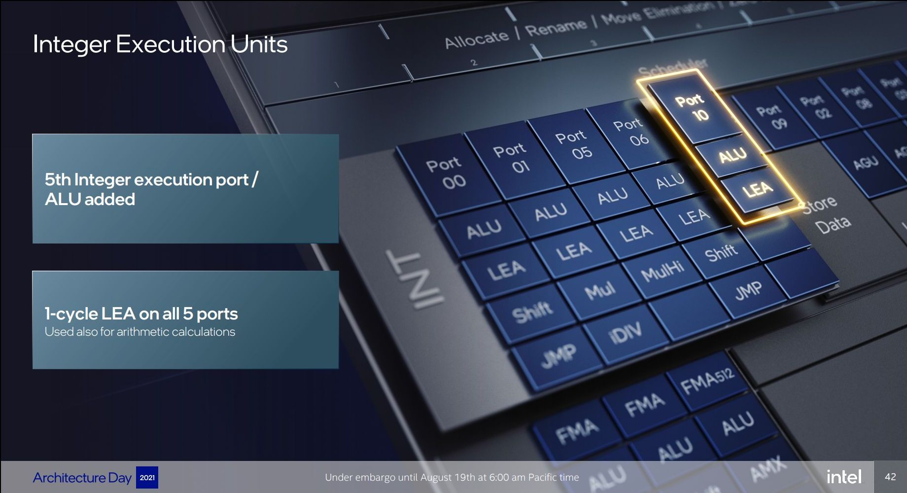
On the integer side of things, there’s now a fifth execution port and pipeline with simple ALU and LEA capabilities, which in theory makes this the widest x86 core in raw ALU throughput, although in mixed code the 5 pipelines are still somewhat comparatively narrower.
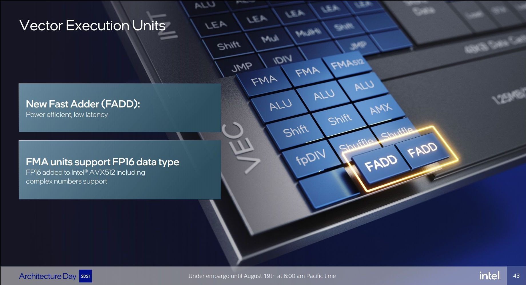
On the FP capabilities side of things, we’ve seen added dedicated FADD capabilities, which are far more efficient and lower latency than using the FMA units (when applicable). The FMA units now have also seen added support for FP16 data types, although this falls under the AVX512 umbrella consumer cores won’t see the capabilities.
In general, besides the added 5th ALU port/pipeline, the back-end execution resources of Golden Cove appear to be somewhat more conservative compared to the more substantial front-end changes of the core.
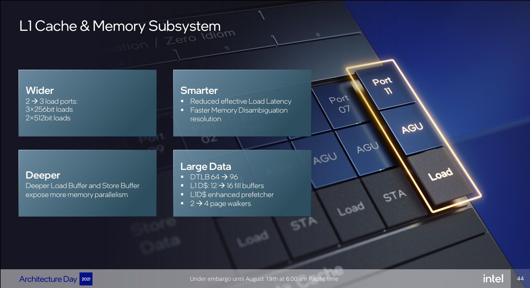
On the load & store front, we see the addition of an additional dedicated execution port with a load AGU, increasing the possible number of loads per cycle from 2 to 3, matching the upgrades we’ve seen from many other microarchitectures over the last few years.
For AVX512-enabled implementations of the µarch, it’s able to load up to 1Kb/cycle from the L1, while consumer cores still see a 50% improvement for AVX2 256-bit loads with 3 per cycle.
Intel, like many other, have noted that modern workloads have increased memory level parallelism, so they have increased the outstanding memory transactions from the core by increasing the L1D fill buffers from 12 to 16, and increasing the load and store buffers by undisclosed amounts. Similarly, to AMD, to better address sparse memory access workloads, the µarch has seen a doubling of page walkers from 2 to 4, able to look up pages in TLB misses.
The L1 DTLB has grown from 64 entries to 96 entries – Intel didn’t mention the L2 TLB which would mean it’s still at 2048 entries.
Intel has improved the prefetchers, nothing things such as “better stride prefetching in L1”, though beyond that the company hasn’t divulged much other details. We’ve seen a lot of advances in the industry in terms of prefetchers so it’ll be interesting to see how Golden Cove compared to the competition here.
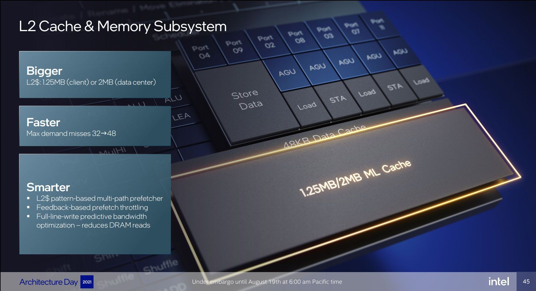
The L2 cache in Golden Cove remains at 1.25MB for consumer core variants, while the server variant grows it to 2MB compared to 1.25MB in the current Ice Lake-SP chips. Parallel data access outstanding requests for the memory subsystem has grown from 32 misses to 48, also further helping with increasing MLP capabilities of the core.
Intel also again notes there’s been prefetching improvements in the L2. What the company calls “full-line-write predictive bandwidth optimisation” is likely the same mechanism we saw in our review of Ice Lake-SP where the core can greatly improve bandwidth by avoiding RFO reads of cache lines that are going to be fully rewritten, which should greatly improve common generic operations such as memory copies.
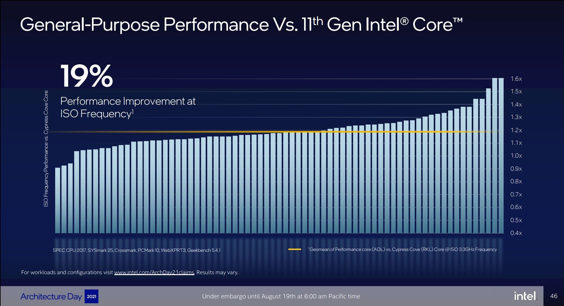
The aggregated changes of the new Golden Cove microarchitecture amount to a geomean IPC increase of 19% compared to Cypress Cove (Rocket Lake) - measured over a set of workloads including SPEC CPU 2017, SYSmark 25, Crossmark, PCMark 10, WebXPRT3, and Geekbench 5.4.1. We can see in the graph that there’s outlier workloads with up to +60% IPC, but also low outliers where the new design doesn’t improve thing much or even sees regressions, which is odd.
The front-end changes of Golden Cove indeed look like a major step-function: 50% wider decode, +25% wider µOP output and double the capacity, +45% deeper out-of-order execution buffer, massive branch prediction improvements. It’s possible that the more conservative back-end execution improvements overall lowered the end results.
19% IPC is still a very impressive figure, and one of Intel’s largest jumps in a decade, but the company is also comparing it to Cypress Cove, rather than their latest generation design, which is Willow Cove inside of the Tiger Lake chips. We would have wished for Intel to at least give us both comparisons, so that we would get an idea for both desktop as well as mobile improvements.


223 Comments
View All Comments
mode_13h - Thursday, August 19, 2021 - link
> On the E-core side, Gracemont will be Intel’s first Atom processor to support AVX2.Finally. It's about f'ing time, Intel.
> desktop processors and mobile processors will now have AVX-512 disabled in all scenarios.
> ...
> If AMD’s Zen 4 processors plan to support some form of AVX-512 ... we might be in
> some dystopian processor environment where AMD is the only consumer processor
> on the market to support AVX-512.
LOL! Exactly! I wouldn't call it "dystopian", exactly. Just paradoxical.
And now that Intel has been pushing AVX-512 adoption for the past 5 years, there should actually be a fair amount of software & libraries that can take advantage of it, making this the worst possible time for Intel to step back from AVX-512! Oh, the irony would be only too delicious!
> Intel is also integrating support for VNNI instructions for neural network calculations.
> In the past VNNI (and VNNI2) were built for AVX-512, however this time around Intel
> has done a version of AVX2-VNNI for both the P-core and E-core designs in Alder Lake.
Wow. That really says a lot about what a discombobulated mess the development of Alder Lake must've been! They thought the E-cores would be a good area-efficient way to add performance, but then AVX-512 probably would've spoiled that. So, then they had to disable AVX-512 in the P-cores. But, since that would hurt deep learning performance too much, they had to back-port VNNI to AVX2!
And then, we're left to wonder how much software is going to bother supporting it, just for this evolutionary cul-de-sac of a CPU (presumably, Raptor Lake or Meteor Lake will finally enable AVX-512 in the E-cores).
Gondalf - Thursday, August 19, 2021 - link
Have you realized this SKU was thinked for 7nm ??....and than backported to 10nm ???.Rocket Lake number two.
TomWomack - Thursday, August 19, 2021 - link
VNNI is four very straightforward instructions (8-bit and 16-bit packed dot-product with/without saturation), so the back port is unlikely to have been difficultmode_13h - Thursday, August 19, 2021 - link
Yeah, but it implies some chaos in the design process.Also, my question about how well-supported it will be stands. I think a lot of people aren't going to go back and optimize their AVX2 path to use it. Any focus on new instructions is likely to focus on AVX-512.
Spunjji - Monday, August 23, 2021 - link
If they kill AVX-512 in consumer with ADL only to bring it back in the next generation, I shall be laughing a hearty laugh. Another round of "developer relations" funding will be needed...Personally I think they never should have brought it to consumer.
mode_13h - Tuesday, August 24, 2021 - link
> I think they never should have brought it to consumer.I have my gripes against AVX-512 (mostly, with regard to the 14 nm implementation), but it's not all bad. I've read estimates that it only adds 11% to the core size of Skylake-SP (excluding the L3 cache slice & such). It was estimated at about 5% of a Skylake-SP compute tile. So, that means less than 5% of the total die size. So, it's probably not coming at too high a price.
Spunjji - Friday, August 27, 2021 - link
That's fair - my reasons for thinking they shouldn't have done it are more related to marketing and engineering effort than die space, though.They put in a lot of time and money to bring a feature to a market that didn't really need it, including doing a load of "developer relations" stuff to develop some cringe-worthy edge-case benchmark results, alongside a bunch of slightly embarrassing hype (including the usual sponsored posters on comment sections), all to lead up to this quiet little climb-down.
Seems like to me like it would have made more sense to designate it as an Enterprise Grade feature - an excuse to up-sell from the consumer-grade "Xeon" processors - and then trickle it down to consumer products later.
mode_13h - Saturday, August 28, 2021 - link
> Seems like to me like it would have made more sense to designate it as an Enterprise> Grade feature ... and then trickle it down to consumer products later.
Yeah, that's basically what they did. They introduced it in Skylake-SP (if we're not counting Xeon Phi - KNL), and kept it out of consumers' hands until Ice Lake (laptop) and Rocket Lake (desktop). It seems pretty clear they didn't anticipate having to pull it back, in Alder Lake, when the latter two were planned.
mode_13h - Saturday, August 28, 2021 - link
BTW, you know the Skylake & Cascade Lake HEDT CPUs had it, right? So, the whole up-sell scheme is what they *actually* did!TristanSDX - Thursday, August 19, 2021 - link
If ADL have disbaled features like part of L2 cache or without AVX-512, so it is interesting if presented 19% IPC growth apply to ADL or SPR.AMD Zen 3 will definitelly have AVX-512, BIG shame on you, for disabling it, even for SKU without small cores