Hot Chips 2021 Live Blog: Graphics (Intel, AMD, Google, Xilinx)
by Dr. Ian Cutress on August 24, 2021 5:20 PM EST- Posted in
- GPUs
- AMD
- Intel
- Edge
- Trade Shows
- Xilinx
- Live Blog
- 7nm
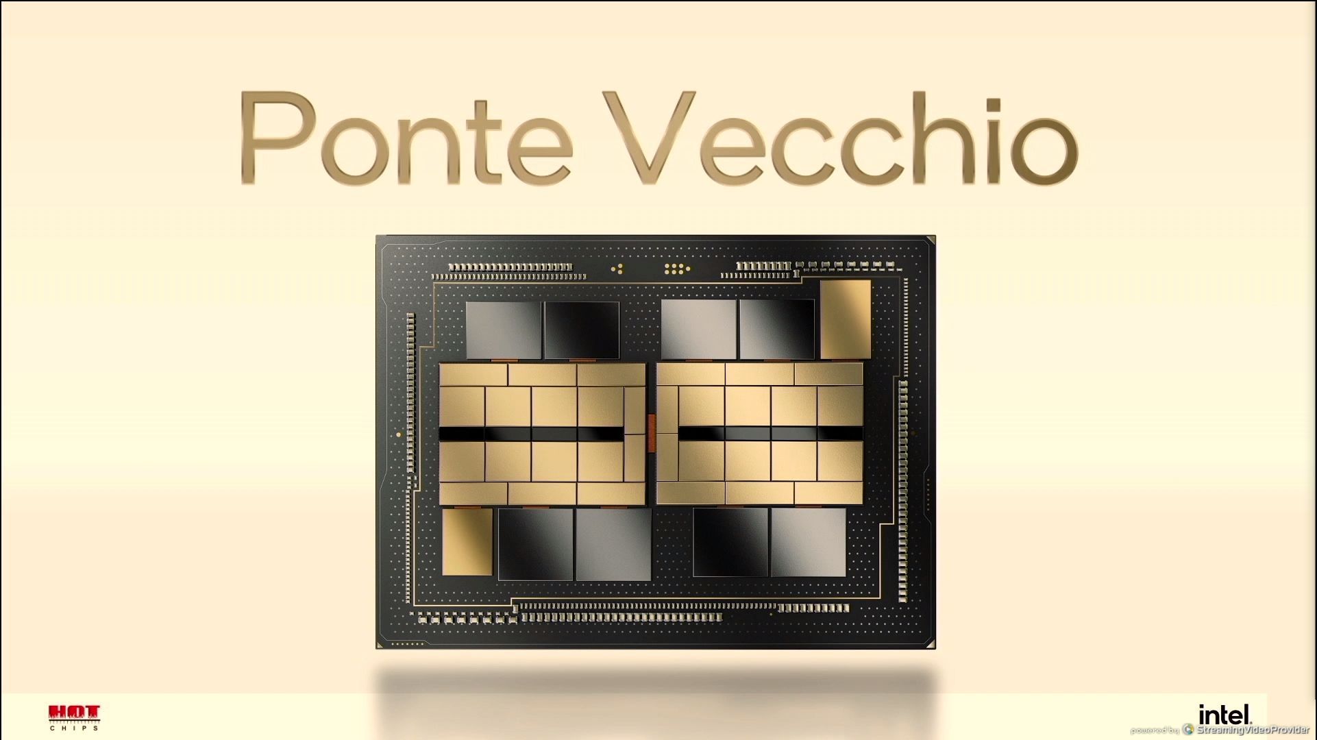
- Ponte Vecchio
- RDNA2
- Hot Chips 33
- VCU
05:28PM EDT - Welcome to Hot Chips! This is the annual conference all about the latest, greatest, and upcoming big silicon that gets us all excited. Stay tuned during Monday and Tuesday for our regular AnandTech Live Blogs.
05:31PM EDT - Stream is starting! We have Intel, AMD, Google, Xilinx

05:32PM EDT - One of the most complex projects at Intel

05:33PM EDT - Aiming for 500x over Intel's previous best GPU
05:33PM EDT - Scale is very important
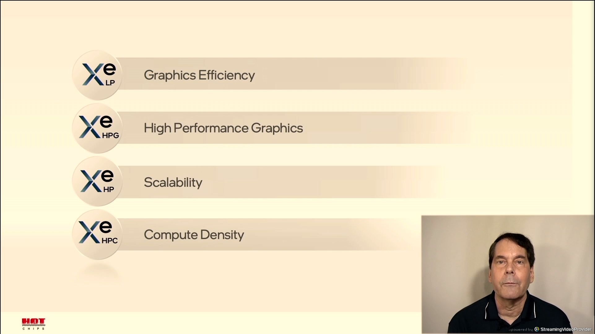
05:33PM EDT - Four variants of Xe
05:34PM EDT - Exascale market needs scale
05:34PM EDT - broad set of datatypes
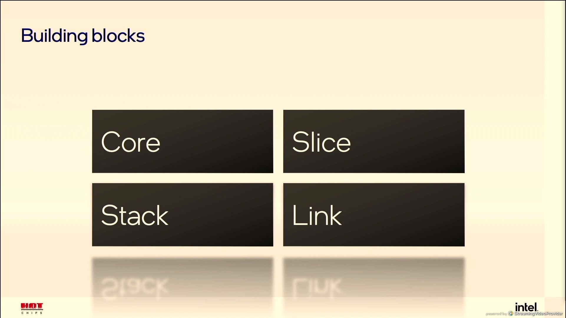
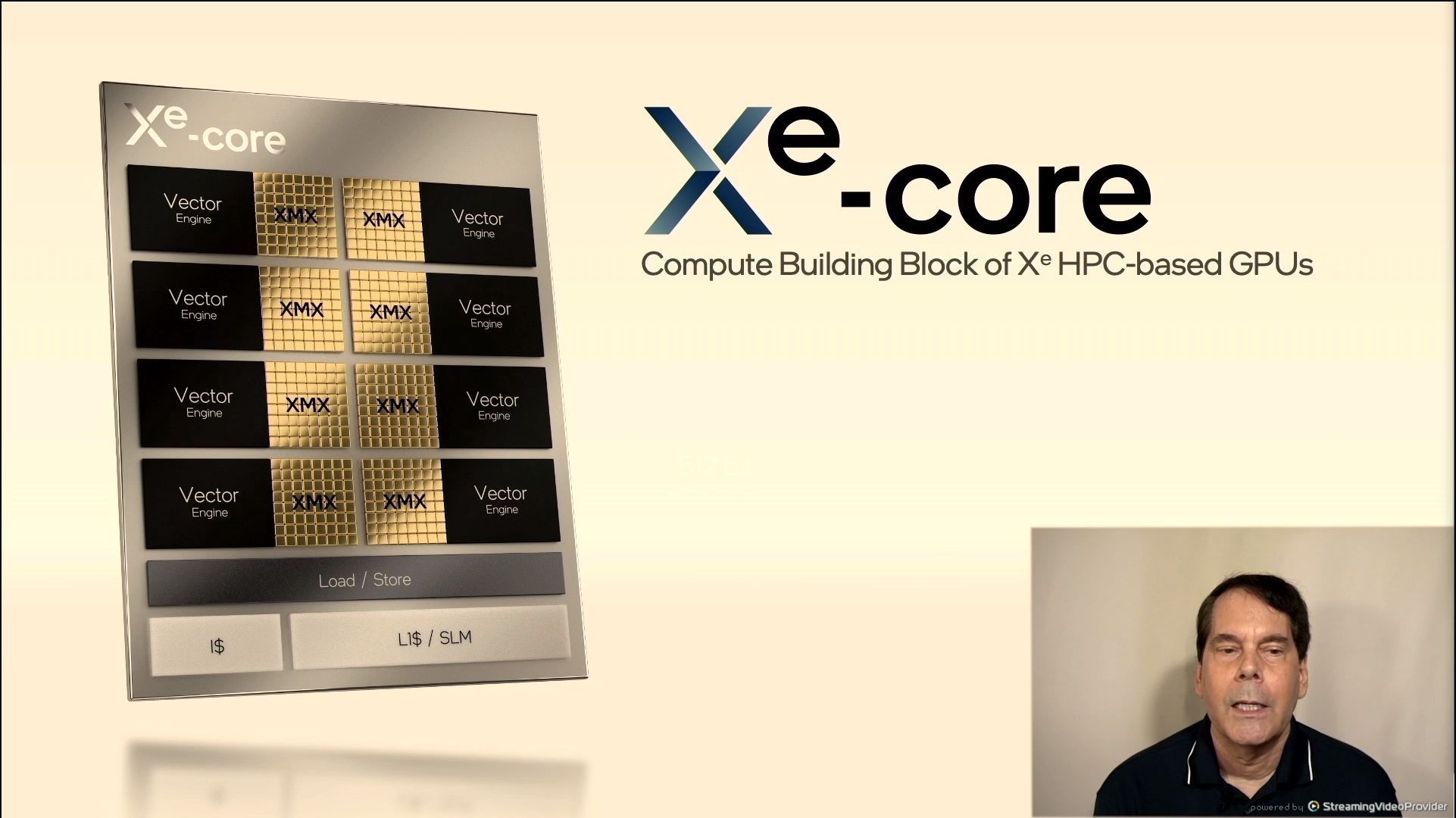
05:34PM EDT - Xe-Core
05:34PM EDT - No longer EUs - Xe Cores now
05:35PM EDT - Each core in HPC has 8x 512-bit vectors, 8x4096-bit matrix engines, 8-deep systloic array
05:35PM EDT - Large 512 KB L1 cache per Xe Core
05:35PM EDT - Software configurable scratch pad shared memory
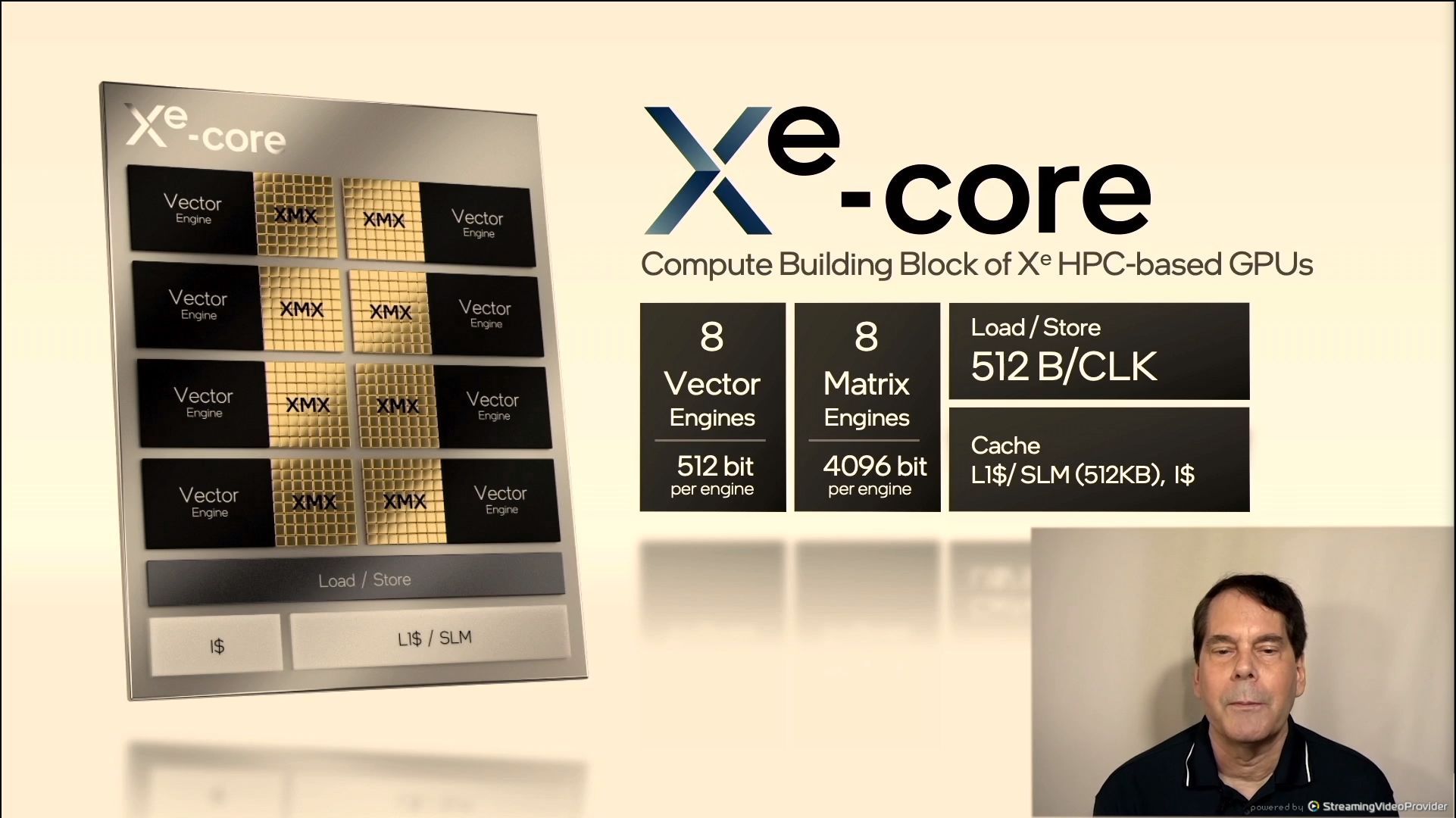
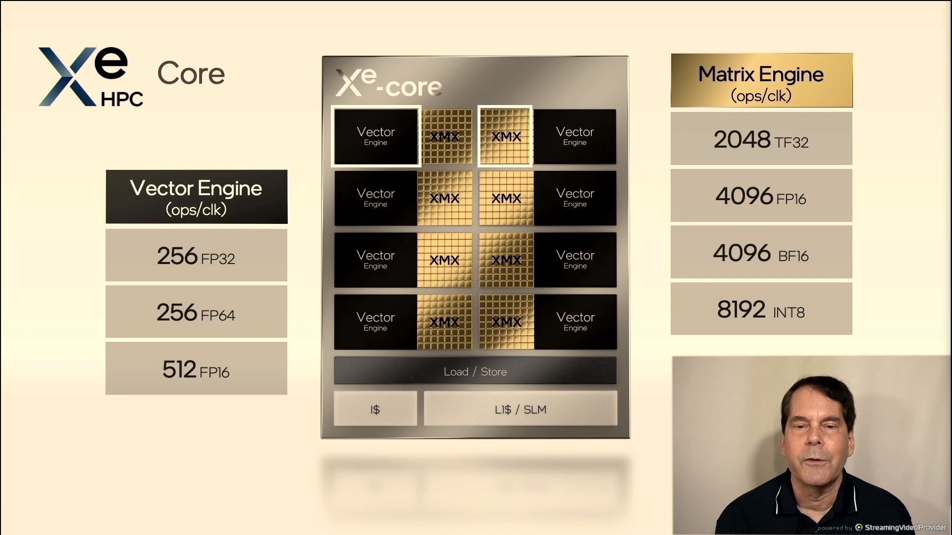
05:36PM EDT - 8192 x INT8 per Xe-Core
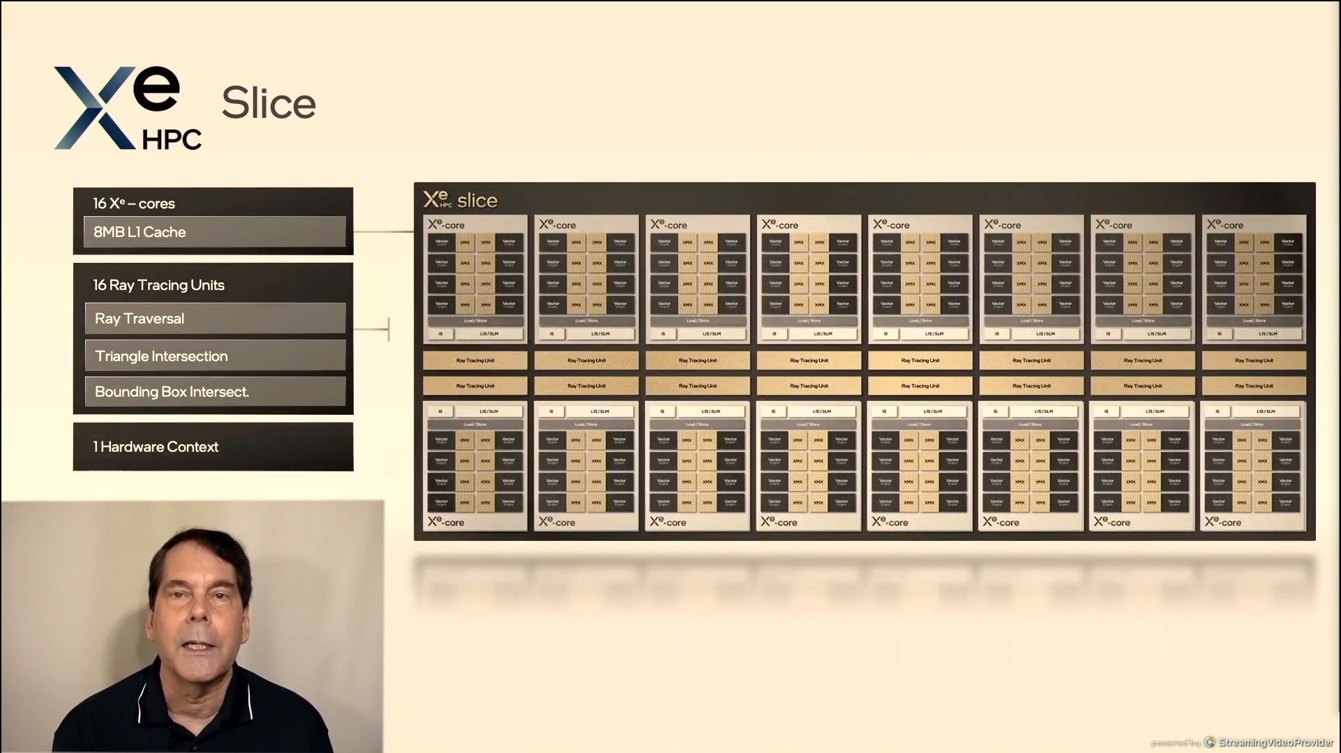
05:36PM EDT - One slice has 16 Xe Cores, 16 RT units, 1 hardware context
05:36PM EDT - ProVis and content creation
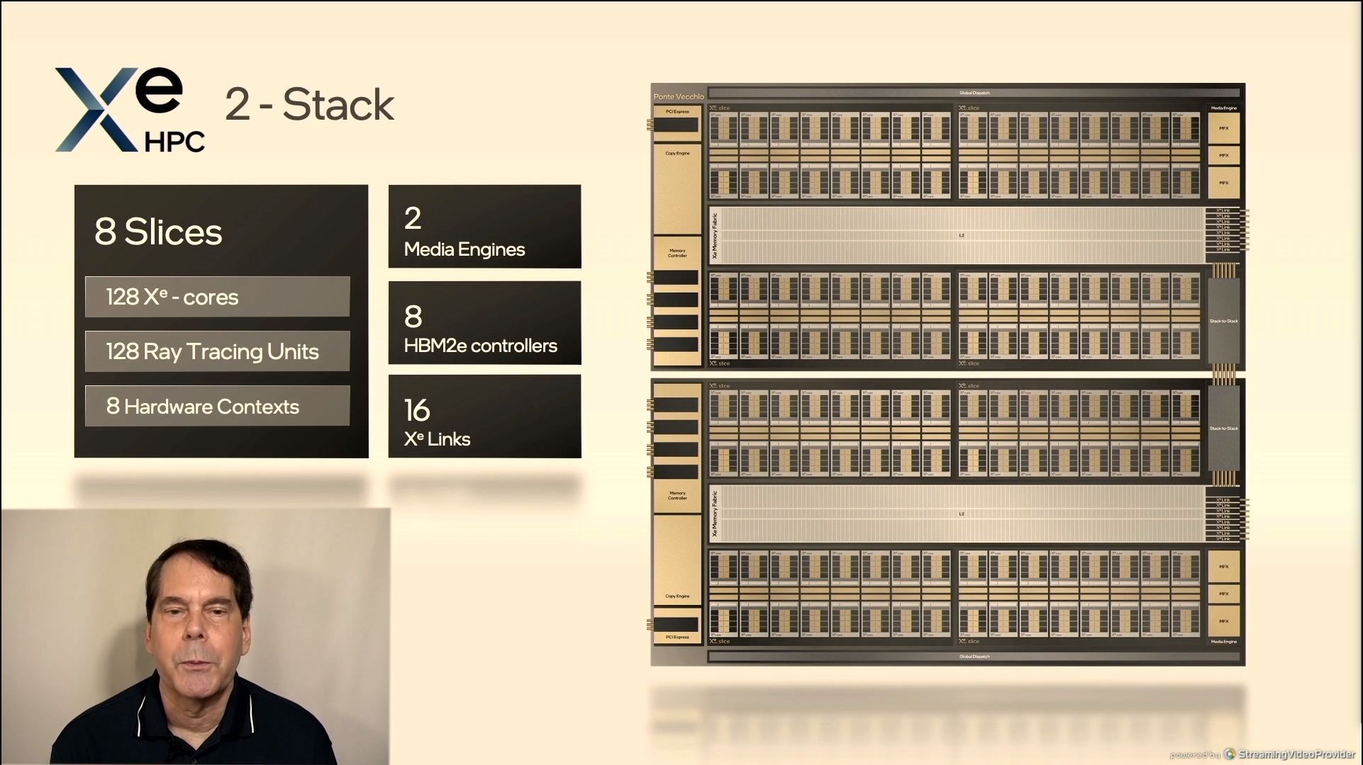
05:37PM EDT - Stack is four Slices
05:37PM EDT - 64 Xe Cores, 64 RT Units, 4 hardware contextsd, L2 cache, 4 HBM2e controllers
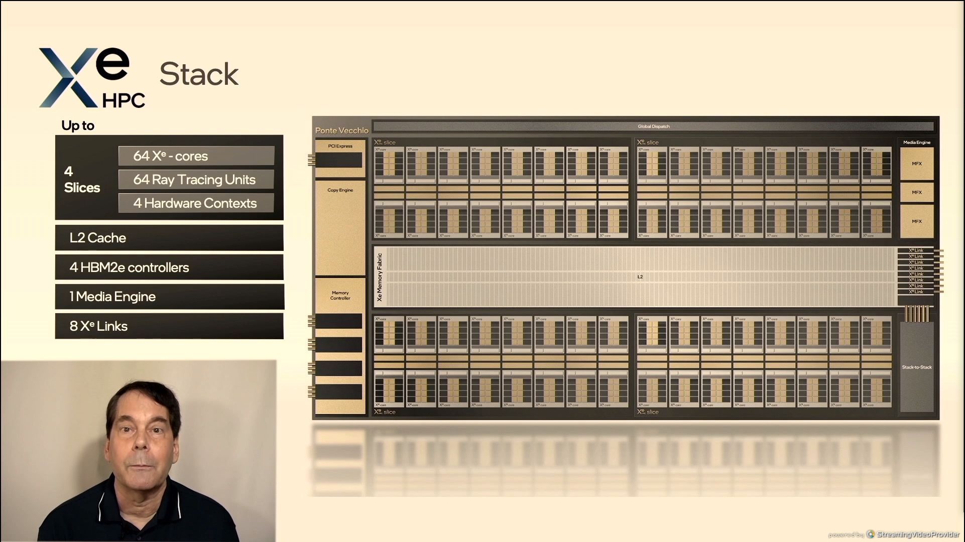
05:37PM EDT - 8 Xe Links
05:37PM EDT - Support 2 stacks
05:38PM EDT - connected directly through packaging

05:38PM EDT - GPU to GPU communication
05:38PM EDT - 8 fully connected GPUs through embedded switch
05:38PM EDT - not for CPU-to-GPU
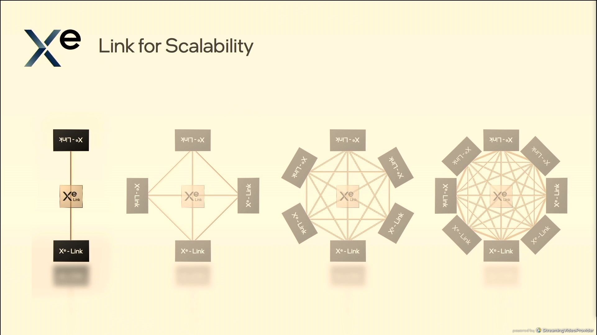
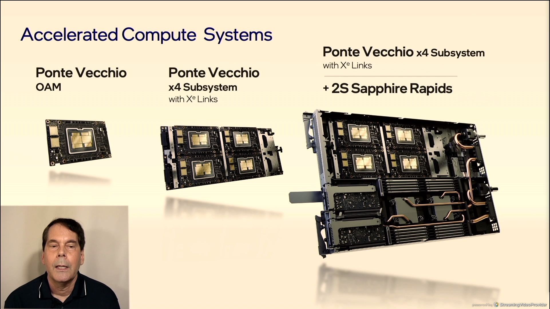
05:39PM EDT - 8 GPUs in OAM
05:39PM EDT - OCP Accelerator Module
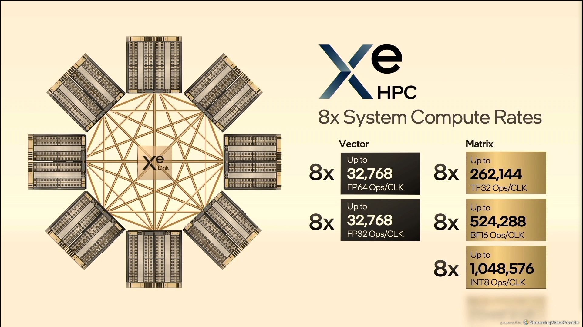
05:39PM EDT - 1 million INT8/clock in one system
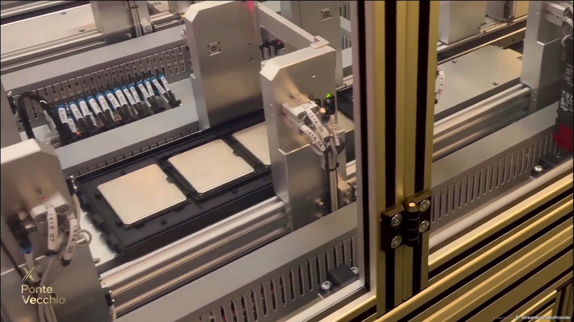
05:40PM EDT - Advanced packaging

05:41PM EDT - Lots of new stuff
05:41PM EDT - EMIB + Foveros

05:41PM EDT - 5 different process nodes
05:42PM EDT - MDFI interconnect traffic
05:42PM EDT - lots of challenges

05:42PM EDT - Learned a lot
05:43PM EDT - Floorplan locked very early
05:43PM EDT - Run Foveros at 1.5x frequency initially thought to minimize foveros connections
05:43PM EDT - booted a few days after first silicon back
05:44PM EDT - Order of magnitude more Foveros connections than other previous designs
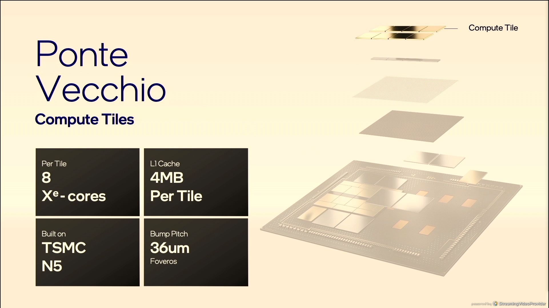
05:44PM EDT - Compute tiles built on TSMC N5
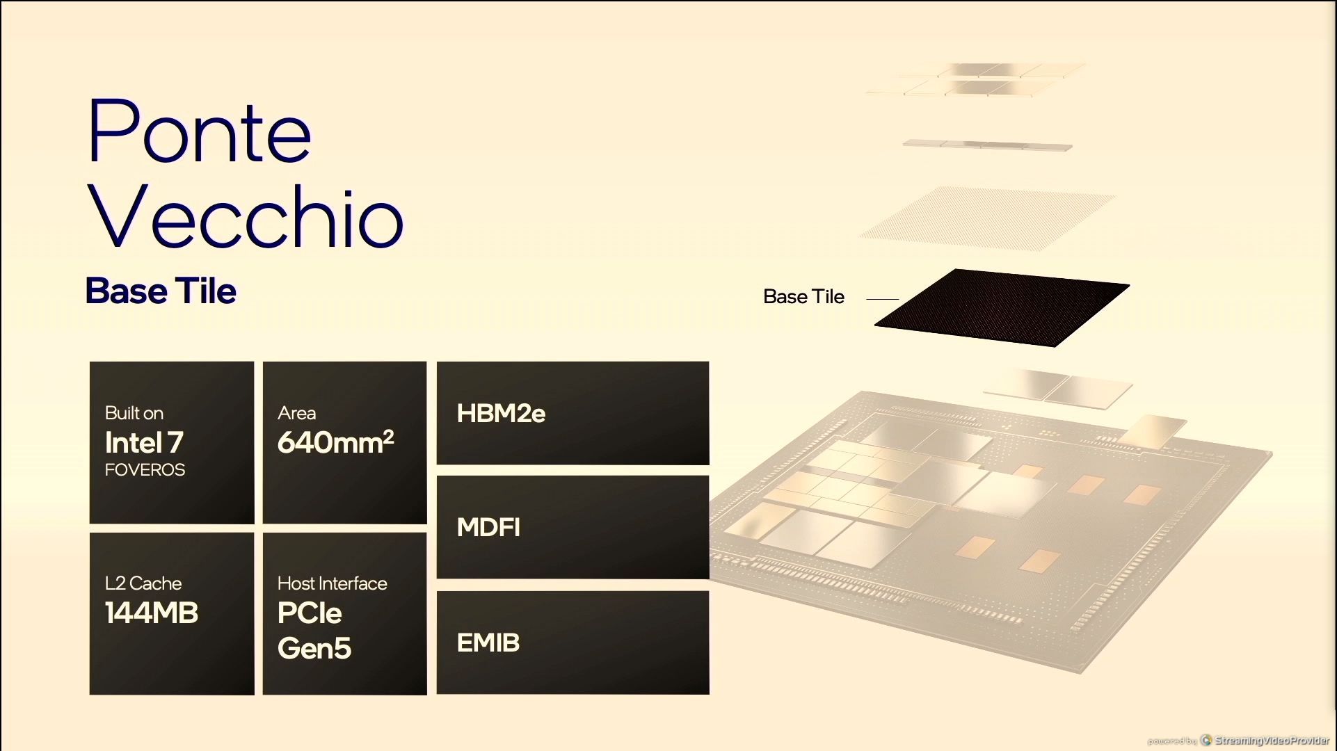
05:45PM EDT - 640mm2 per base tile, built on Intel 7
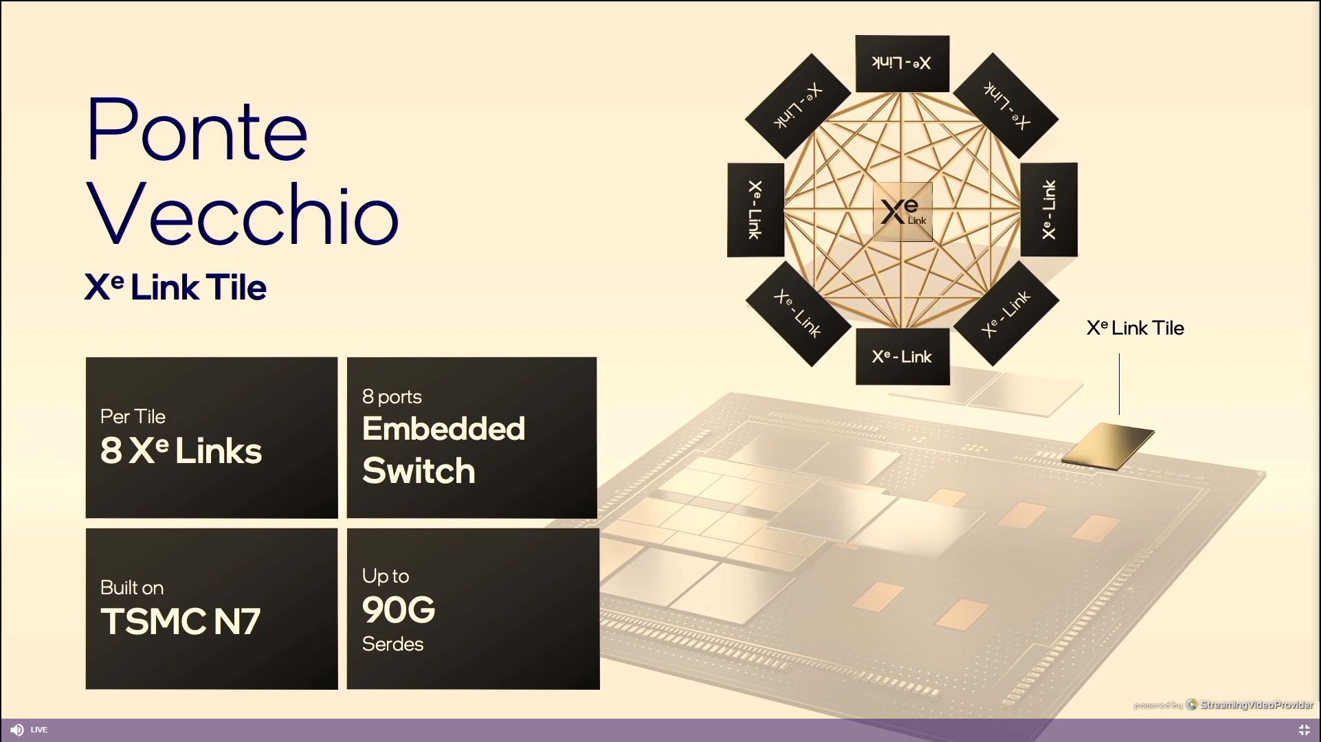
05:46PM EDT - Xe Link Tile built in less than a year
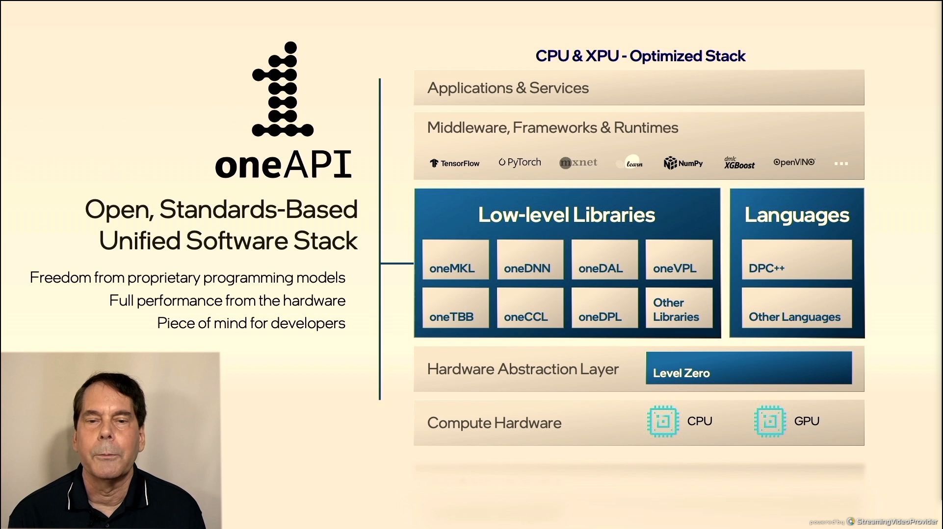
05:47PM EDT - OneAPI support
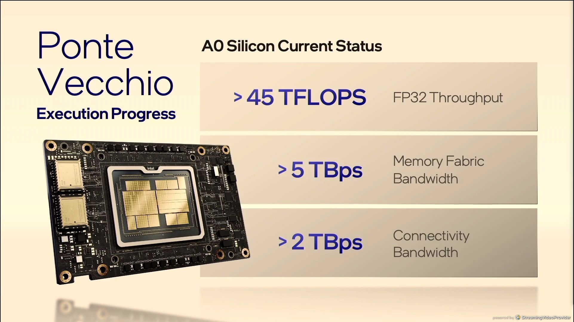
05:47PM EDT - 45 TFLOPs of sustained perf

05:48PM EDT - Customers early next year
05:48PM EDT - Q&A
05:50PM EDT - Q: PV of 45TF FP32 compute - 45 TF of FP64? A: Yes
05:51PM EDT - Q: More insights into hardware context - is 8x PV monolithic or 800 instances? A: Looks like a single logical device, independent applications can run in isolation in context level
05:53PM EDT - Q: Does Xe Link support CXL, if so, which revision? A: nothing to do with CXL
05:54PM EDT - Q: Does the GPU connect to CPU by PCIe or CXL? A: PCIe
05:54PM EDT - Q: Xe Link bandwidth? A: 90G serdes
05:55PM EDT - Q: Peak power/TDP? A: Not disclosing - no product specific numbers
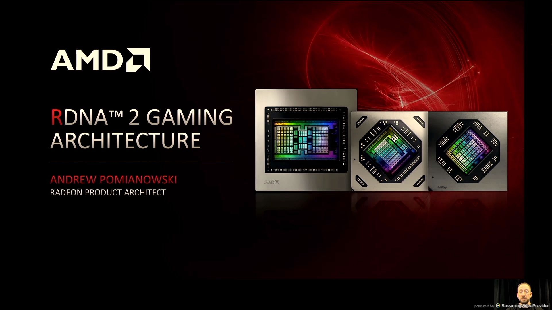
05:55PM EDT - Next talk up is AMD - RDNA2
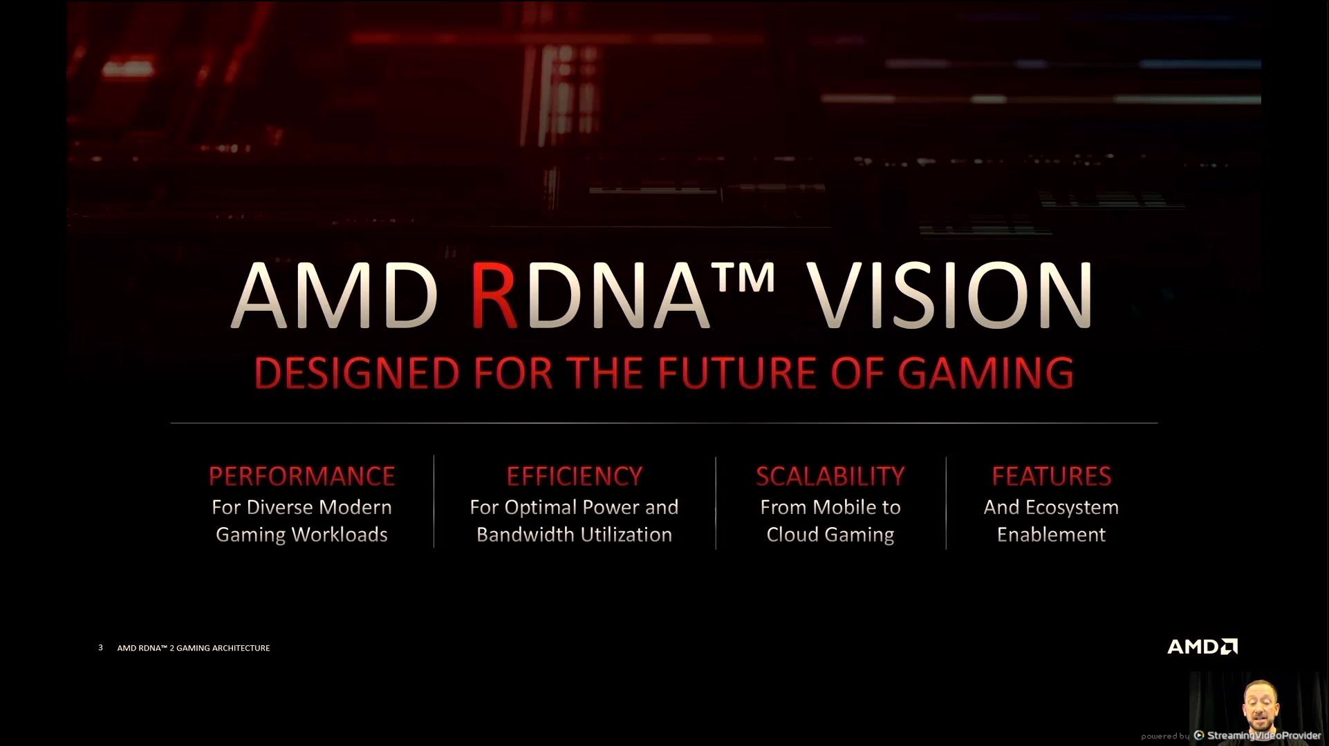
05:57PM EDT - CDNA for compute vs RDNA for gaming
05:57PM EDT - Both are focused on compute for each direction
05:58PM EDT - Flexible and adaptable design
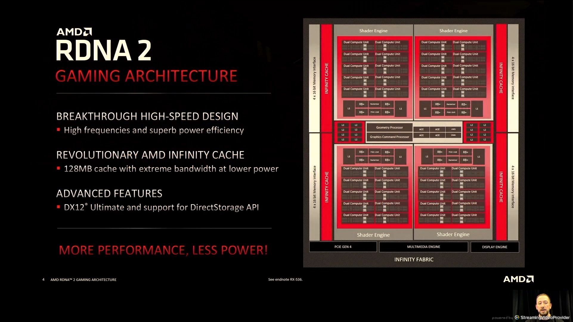
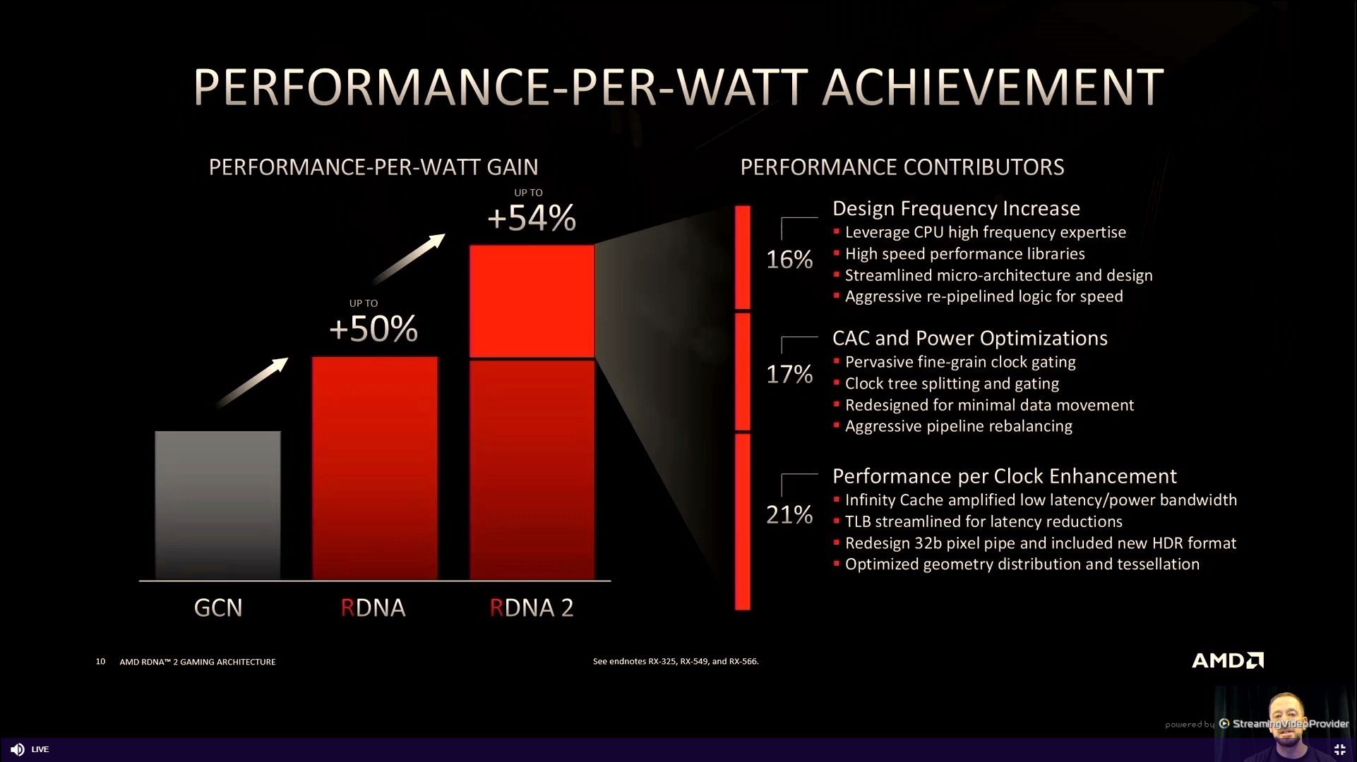
05:58PM EDT - 18 months after first RDNA product
05:59PM EDT - 128 MB of Infinity cache
05:59PM EDT - enhance frequency
05:59PM EDT - RDNA unshackled the design from certain underpinnings of GCN
05:59PM EDT - Perf/W is key metric
05:59PM EDT - minimize wasted power
06:00PM EDT - DX12 Ultimate support, support for DirectStorage
06:00PM EDT - Next gen consoles helped with development of featureset
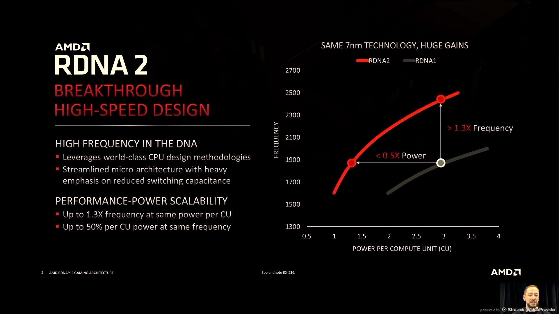
06:01PM EDT - +30% Freq at iso-power, or under half power for isofrequency
06:02PM EDT - All done without change in process node
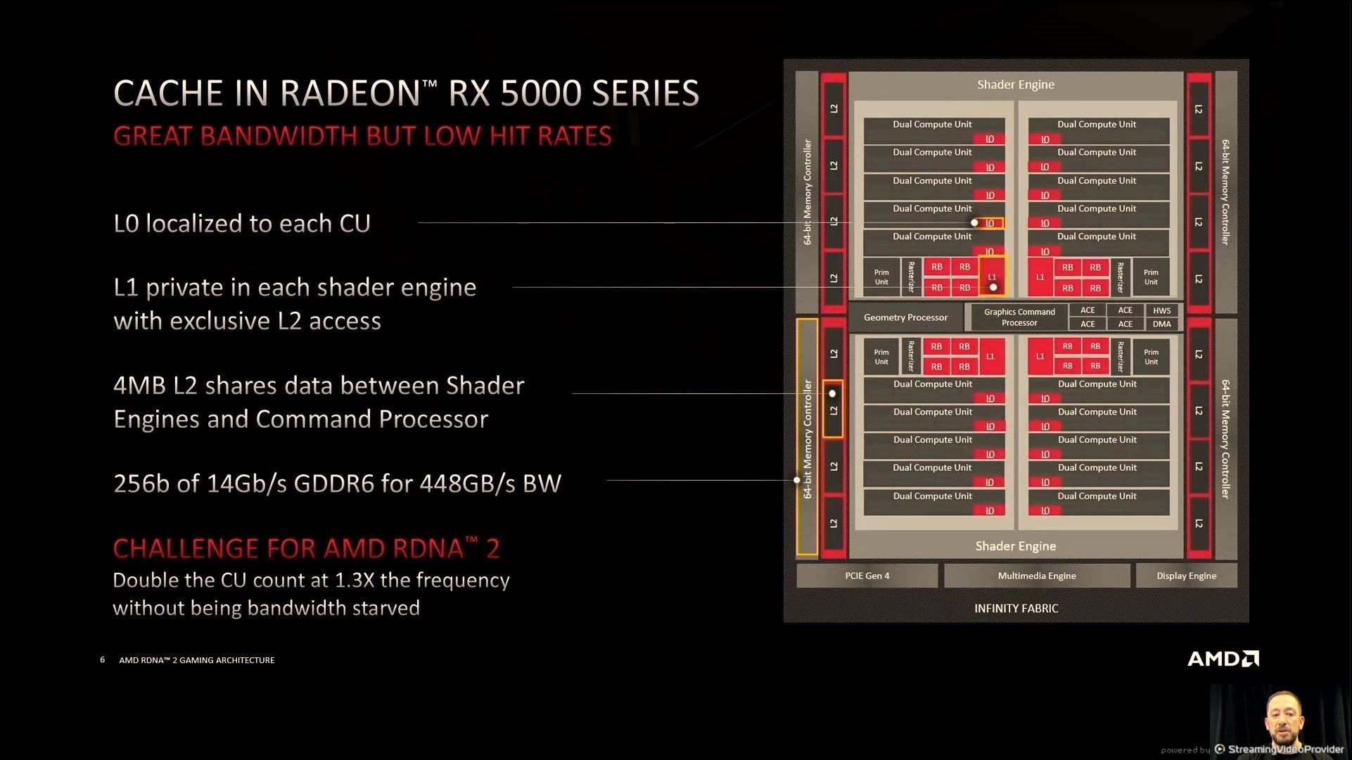
06:03PM EDT - RX5000 - RDNA1 - high bandwidth but low hit rates
06:04PM EDT - Trying to avoid GDDR use to reduce power - so increase caches!

06:04PM EDT - GPU cache hit rates
06:04PM EDT - graphics used to be one-pass compute

06:05PM EDT - Big L3 caches
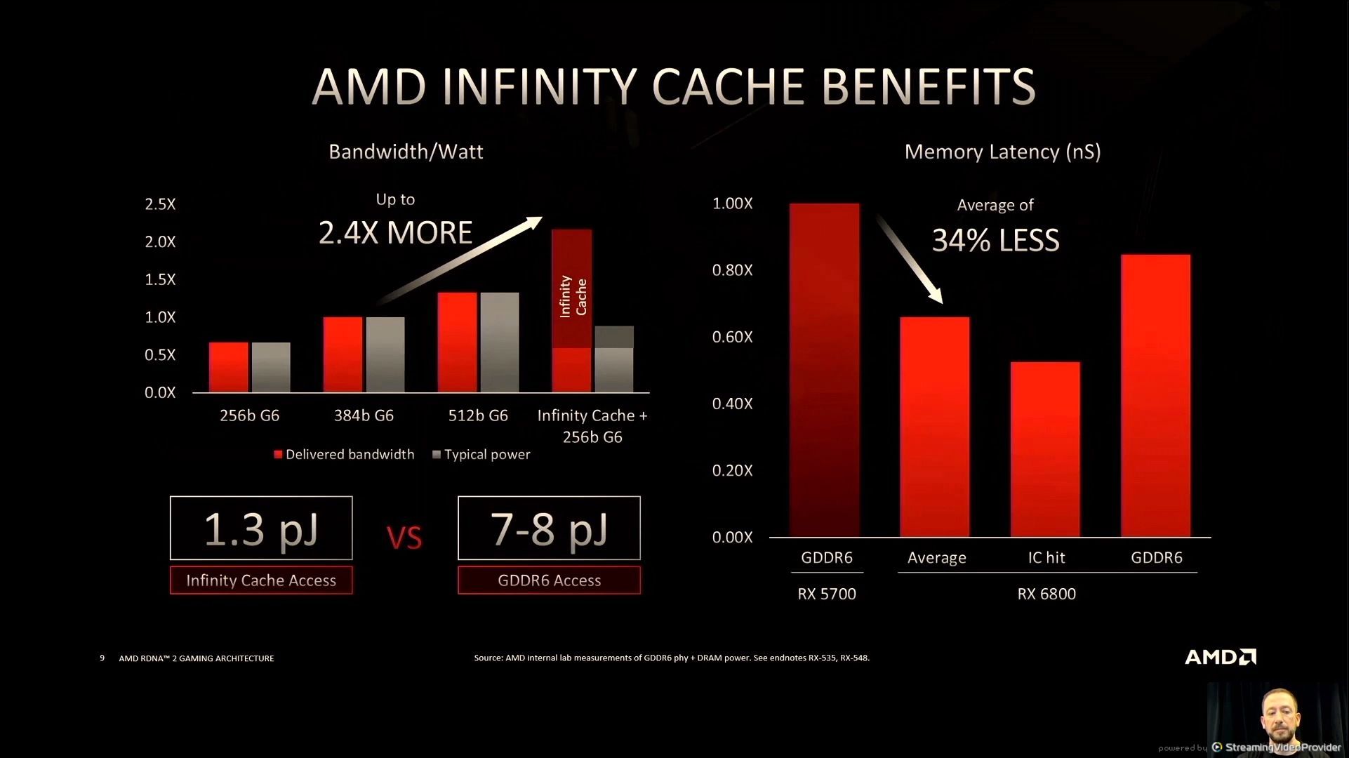
06:07PM EDT - lower energy per bit - only 1.3 pJ/bit on cache vs 7-8 pJ/bit for GDDR6
06:08PM EDT - Average memory latency on RX6800 is 34% lower than RX5700
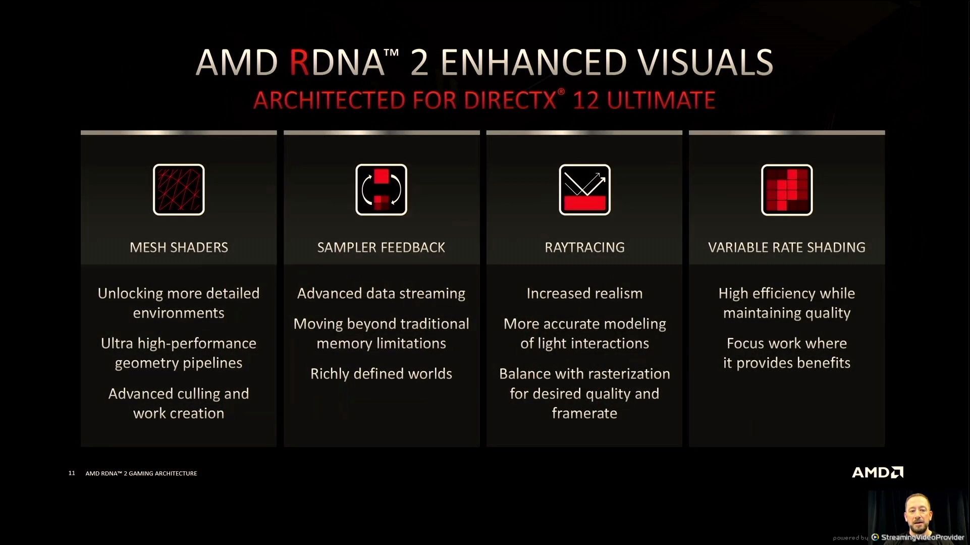
06:10PM EDT - Ray tracing in RDNA2
06:10PM EDT - Variable Rate Shading
06:10PM EDT - Sampler Feedback
06:10PM EDT - Mesh Shaders
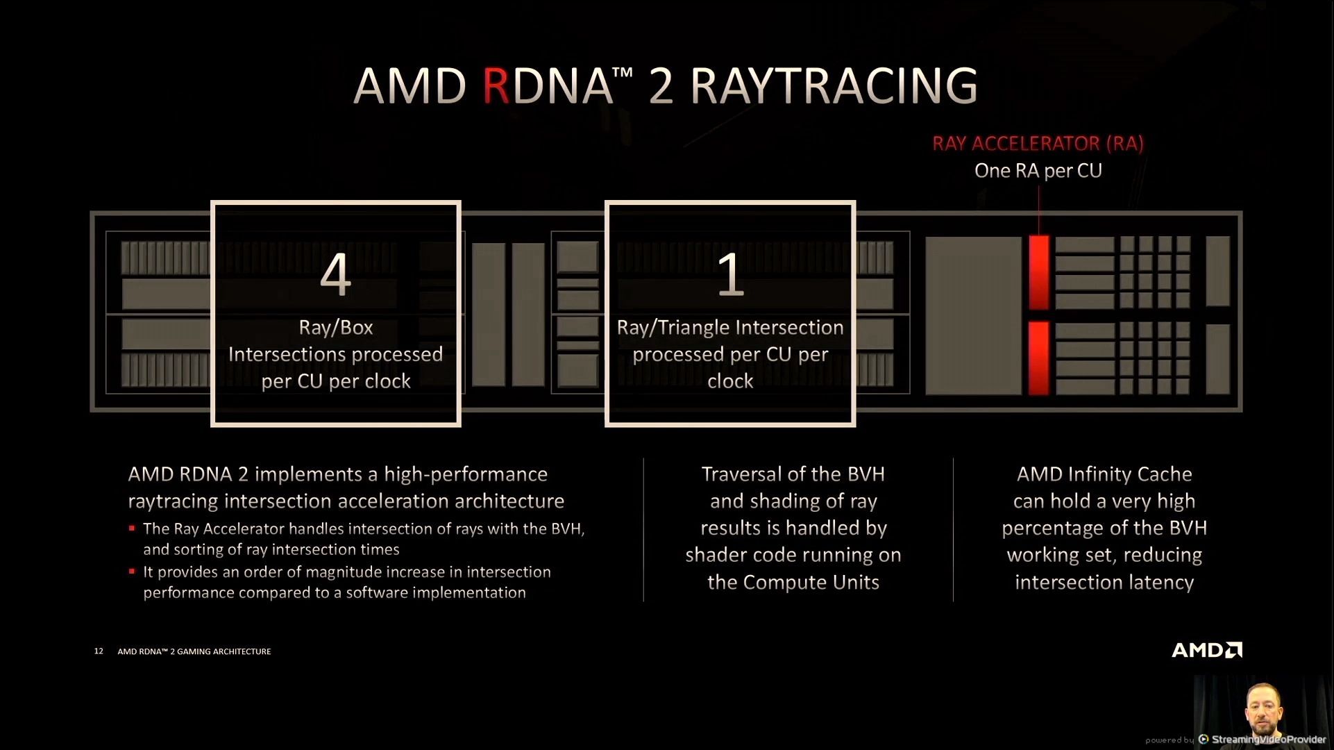
06:11PM EDT - RT aimed to be effficient without adding overhead
06:12PM EDT - tightly integrated into the shader architecture
06:12PM EDT - Streamlined implementation

06:13PM EDT - VRS uses fine grained rate selection per 8x8 pixels
06:13PM EDT - VRS up to 2x2 in an 8x8 grid

06:16PM EDT - Q&A
06:19PM EDT - Q: Why Infinity Cache vs Stacked V-Cache A: Not discussing, were only evaluating on-die cache
06:22PM EDT - Q: TDP % as CUs vs other? A: High workload, most power in CUs - exact breakdown is based on workload - CUs are largest, can exceed 50%, 2nd is GPU common blocks, 3rd DRAM interface. Infinity cache changes 2nd/3rd position. 4th is Infinity Cache
06:23PM EDT - Q: SteamDeck Van Gogh? A: No comment
06:29PM EDT - Google VCU talk
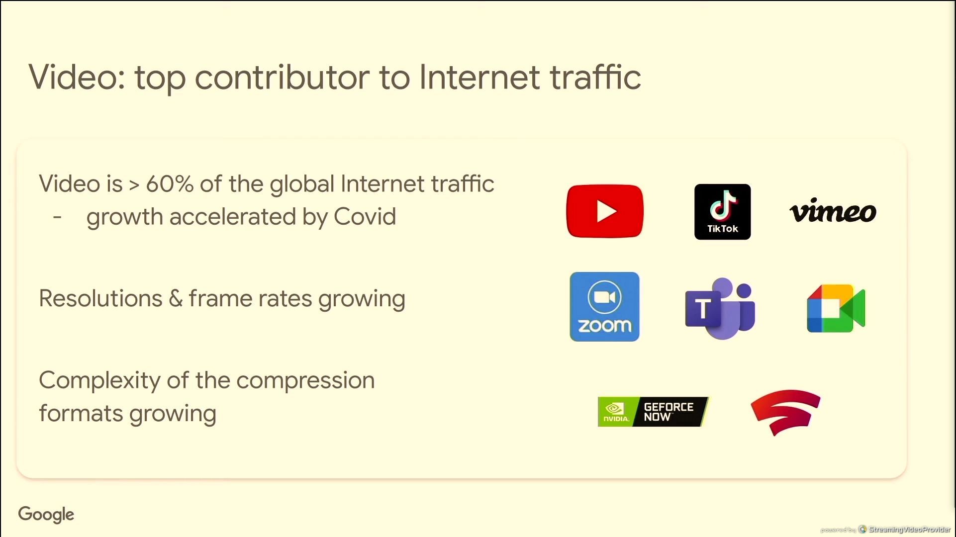
06:30PM EDT - video is >60% of global internet traffic
06:30PM EDT - need better algorithms
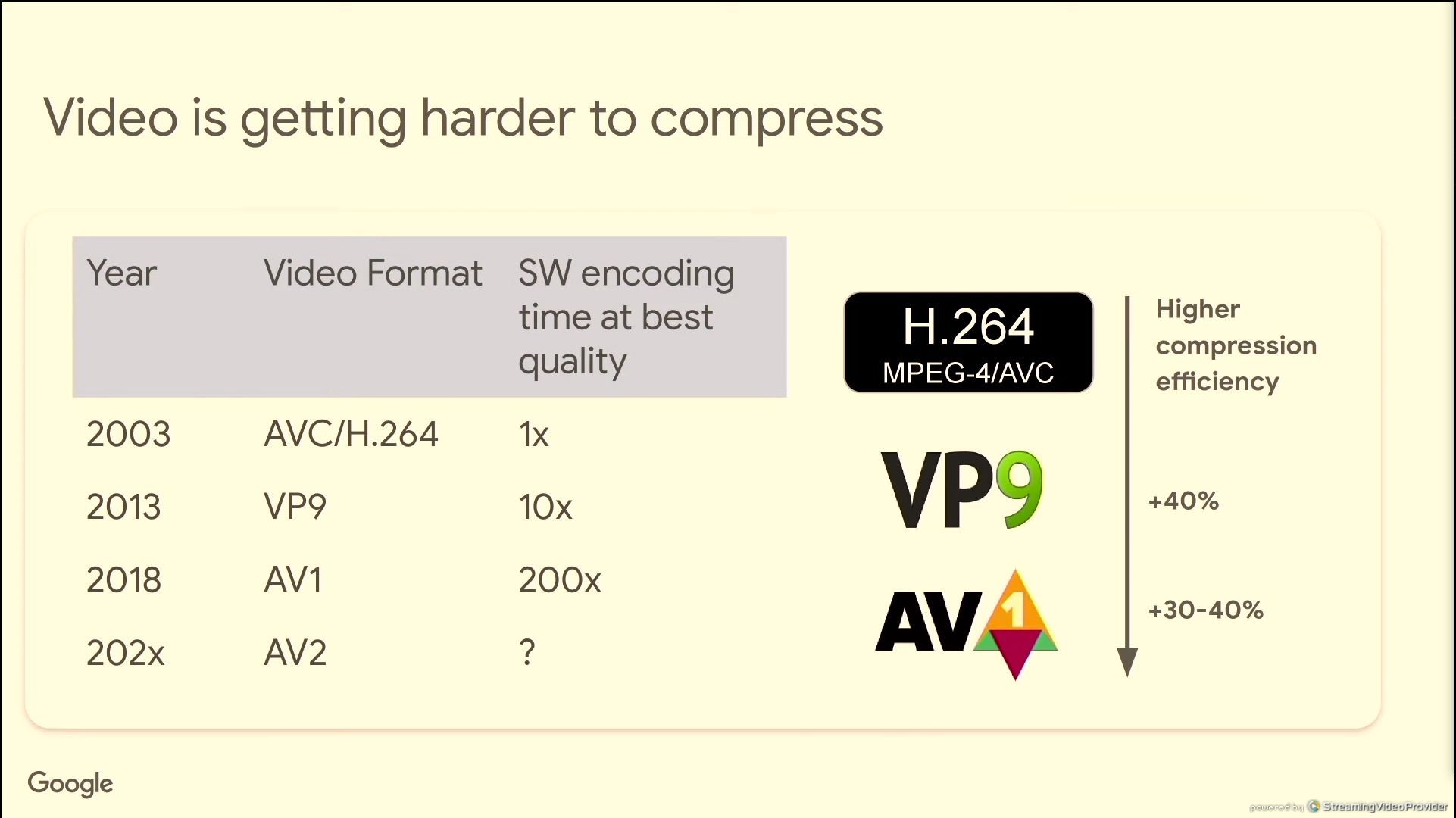
06:30PM EDT - Video is getting hardware to compress
06:31PM EDT - AV1 is 200x more time consuming to encode in software vs H.264
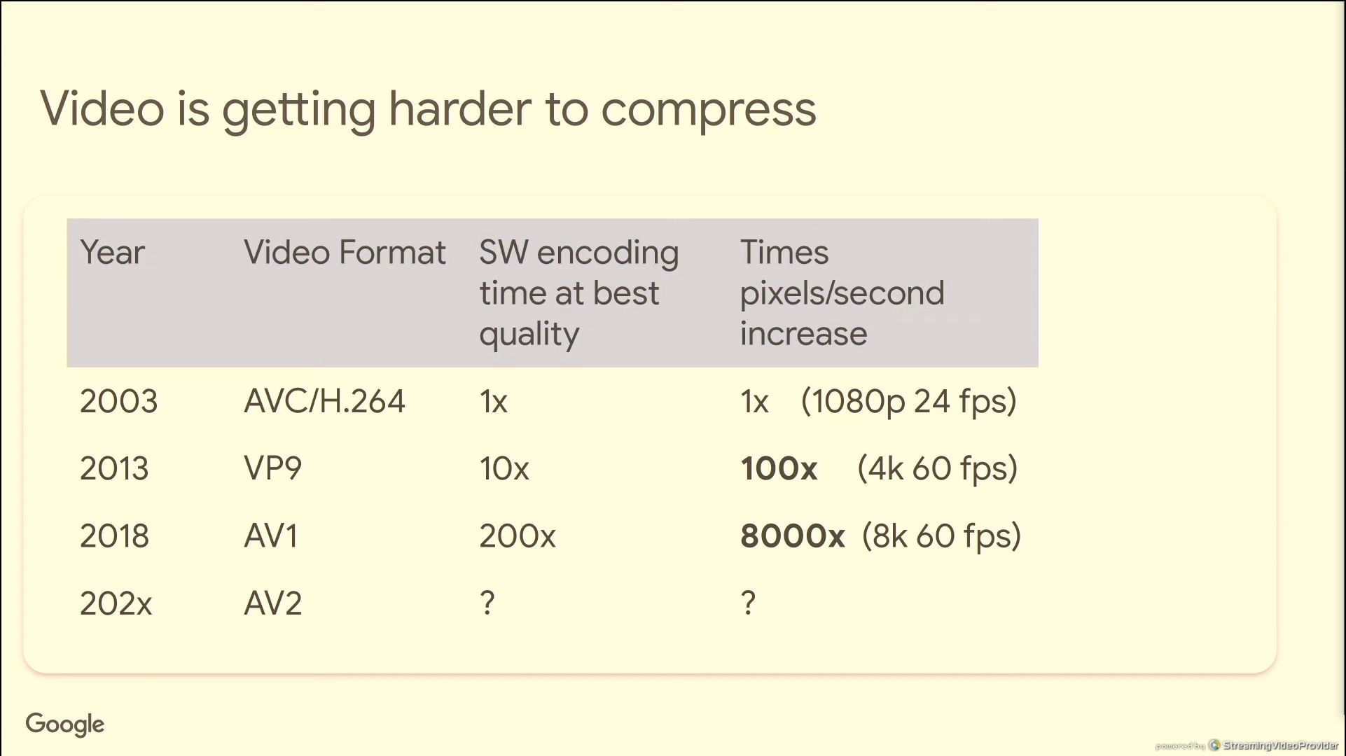
06:31PM EDT - Pixels/second has increased 8000x since H.264
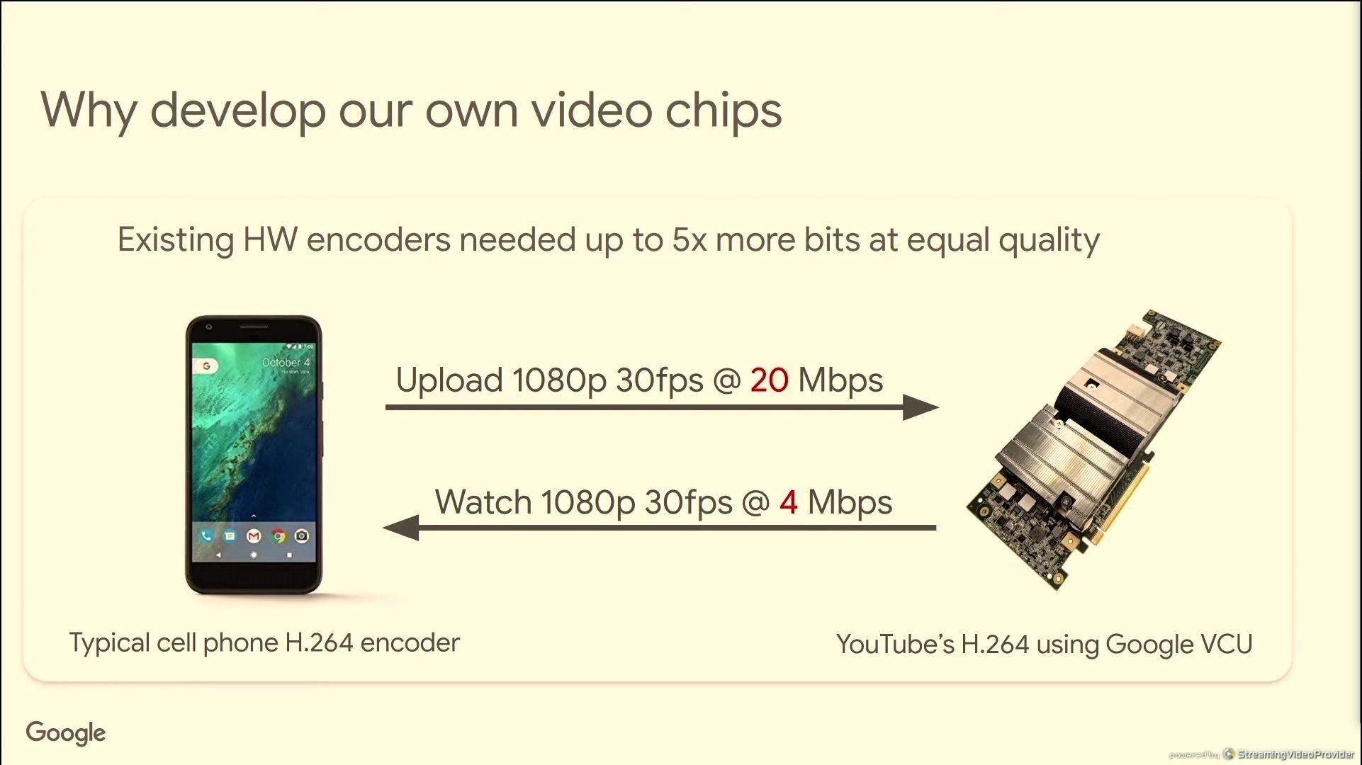
06:32PM EDT - most consumer hardware is optimized for cost, not performance or efficiency
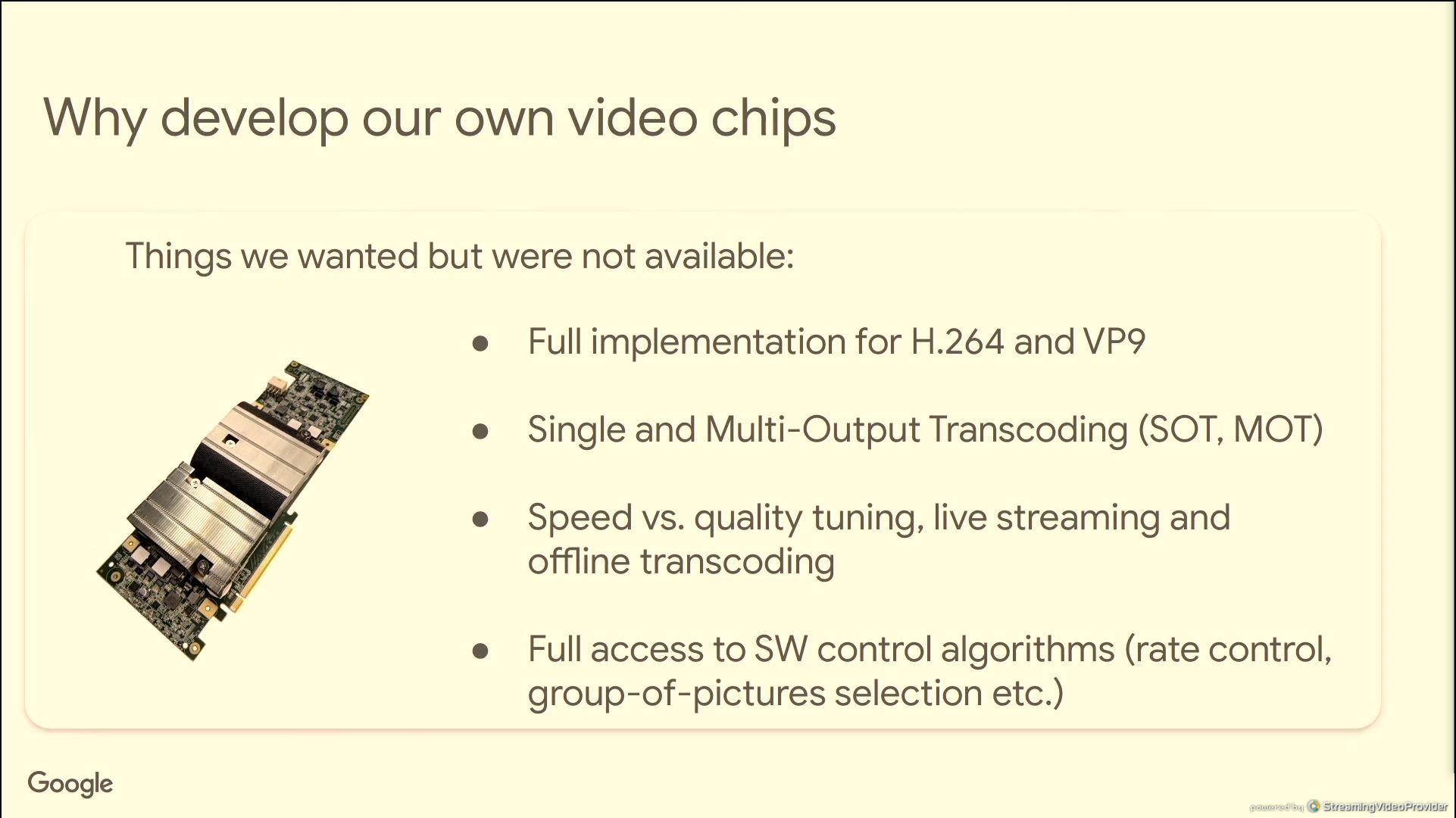
06:32PM EDT - Could not find everything in off the shelf offering
06:32PM EDT - Encode 10s of versions with one input
06:33PM EDT - Need full access to configuration tools
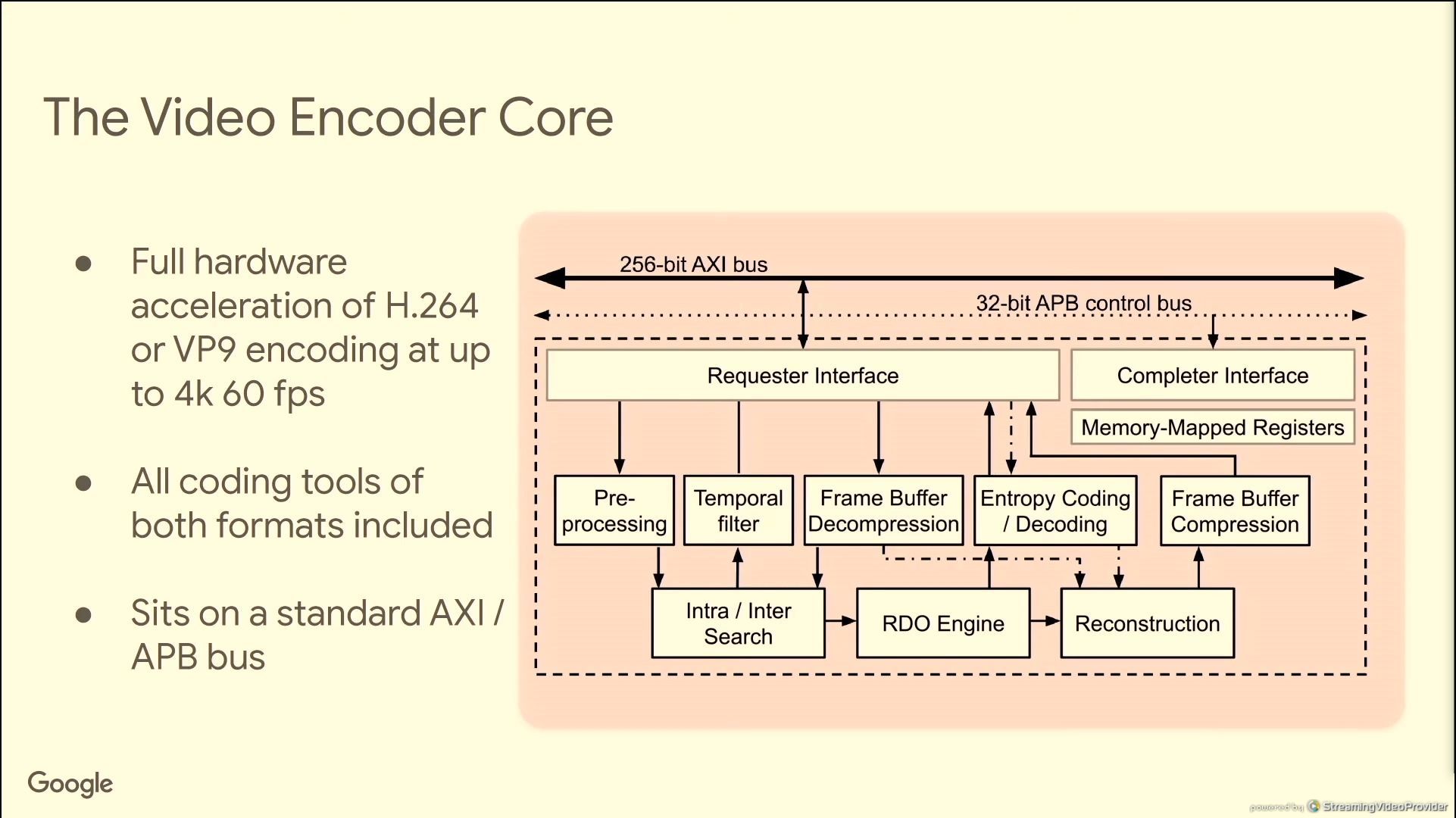
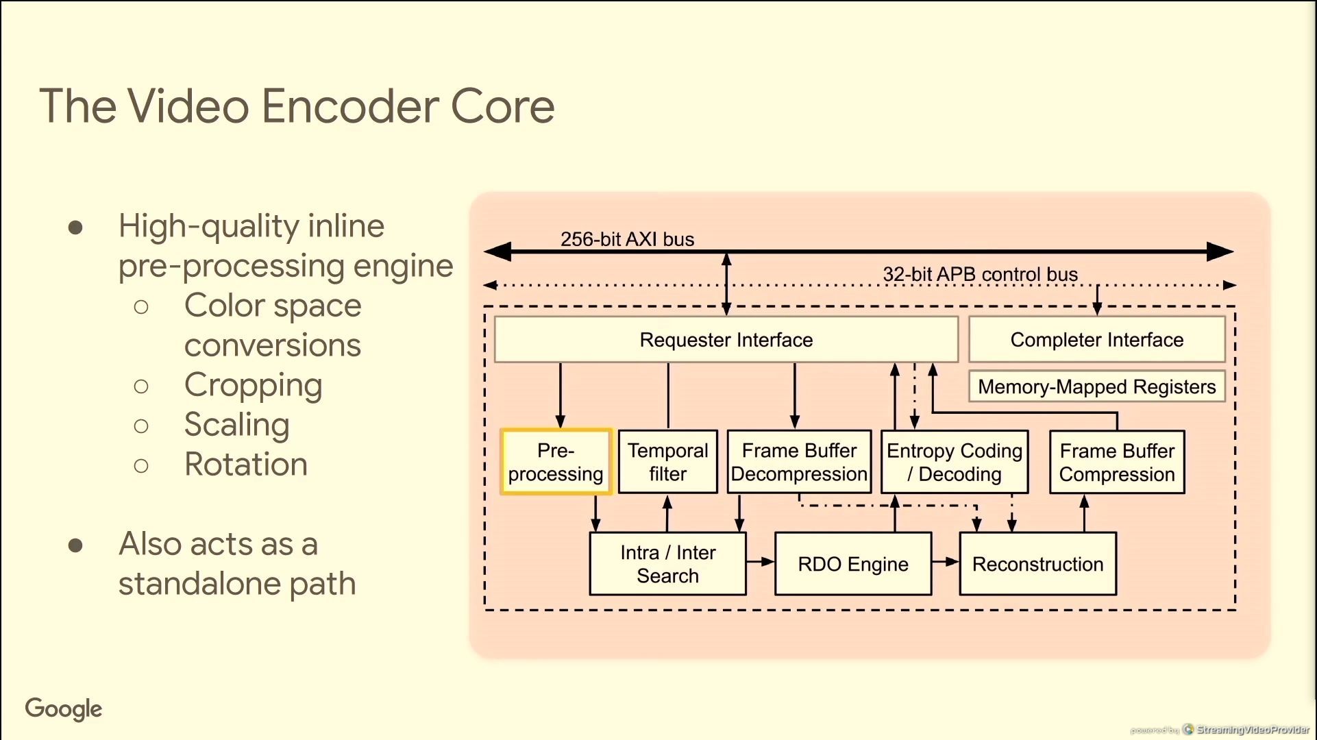
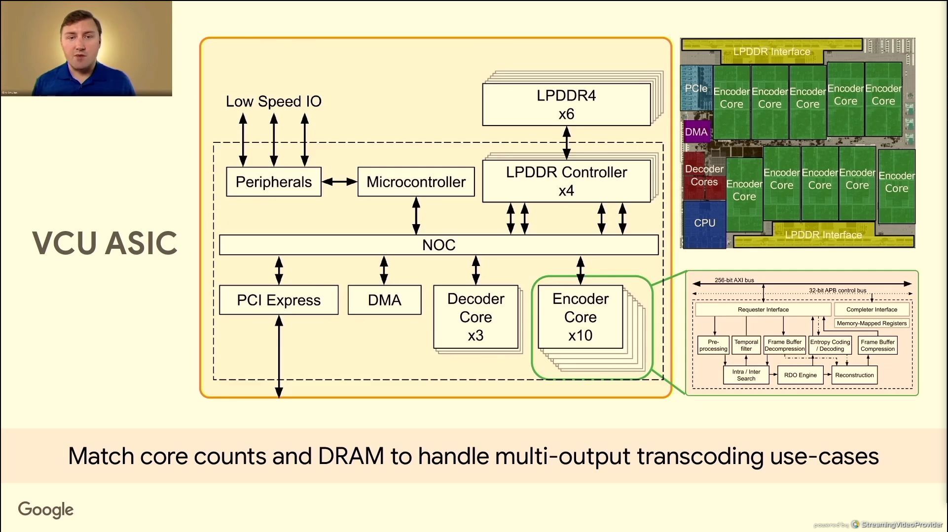
06:34PM EDT - Dedicated VP9 encode and decode
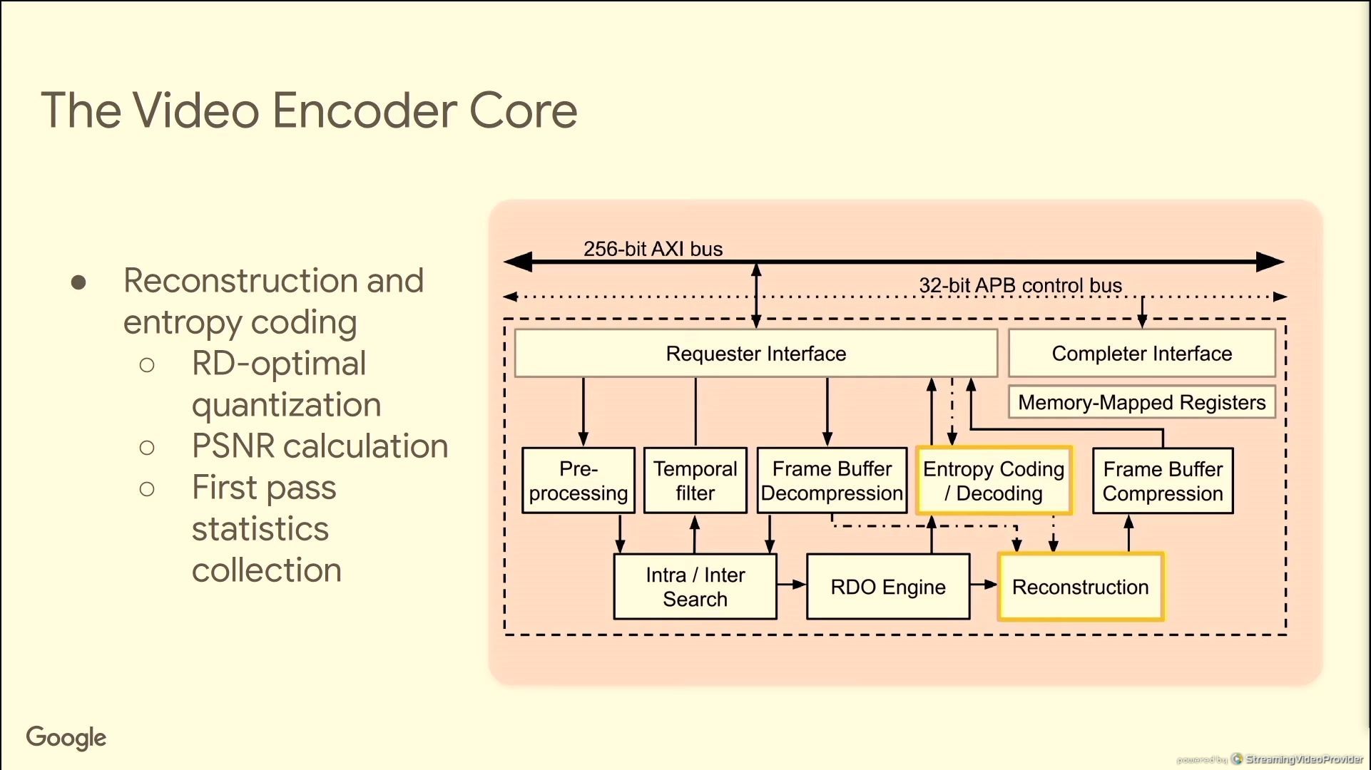
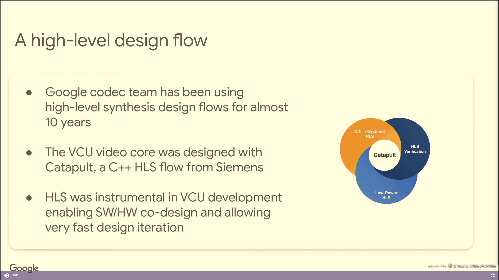
06:36PM EDT - enabling sw/hw codesign
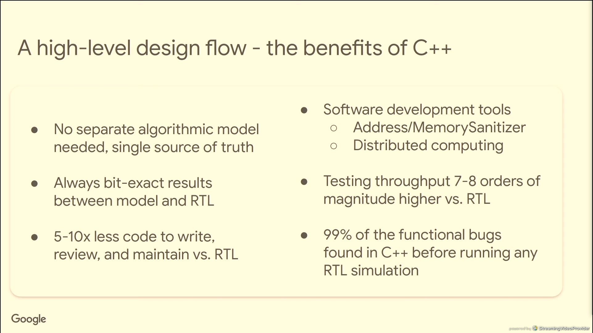
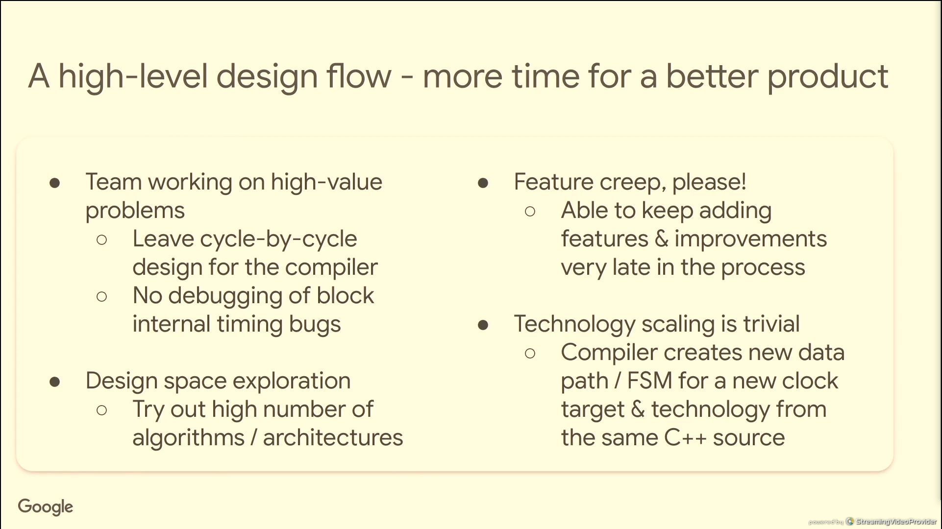
06:38PM EDT - With HLS, allowed them to test lots of architecture variations for features and performance
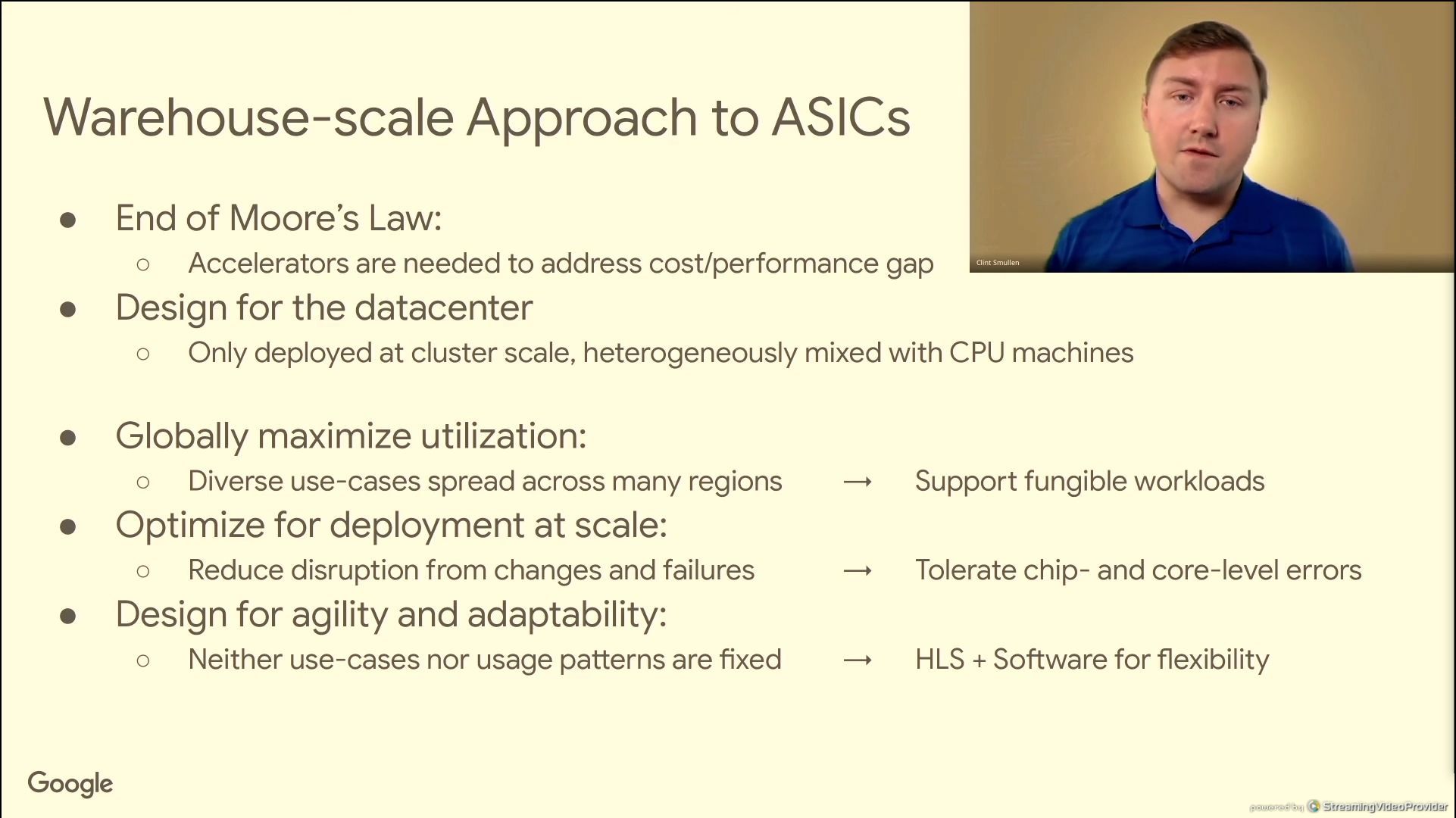
06:39PM EDT - Accelerators need to scale to warehouse scale computing
06:40PM EDT - tolerate errors at chip and core level errors - reliability is a higher level function
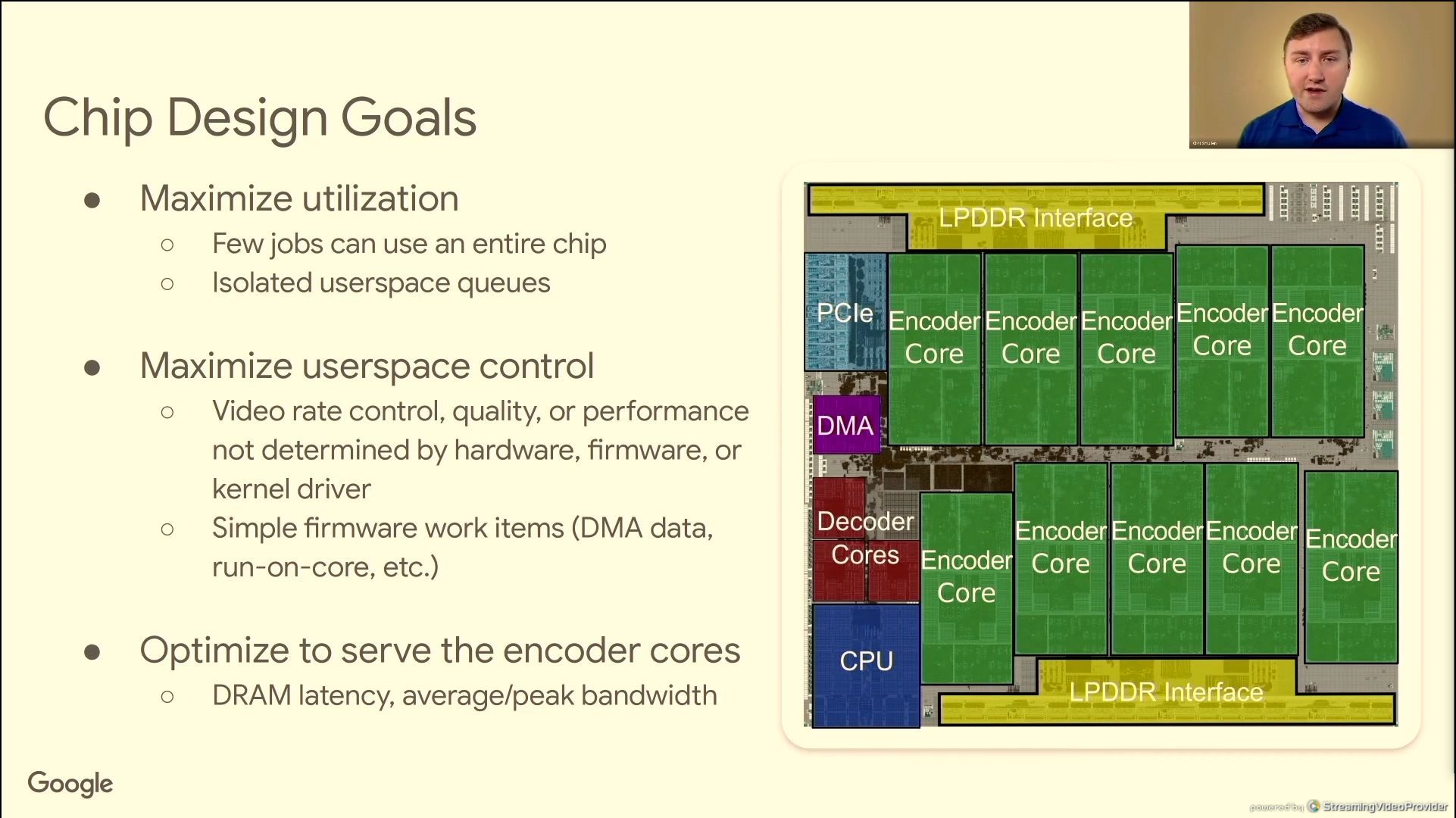
06:40PM EDT - Need to support 48 encodes per decode (MOT)
06:40PM EDT - Upload one video, encode multiple versions
06:41PM EDT - chip level cache was ineffective
06:41PM EDT - core counts to support large MOTs
06:41PM EDT - LPDDR4 for bandwidth per byte
06:41PM EDT - on chip memories use ECC
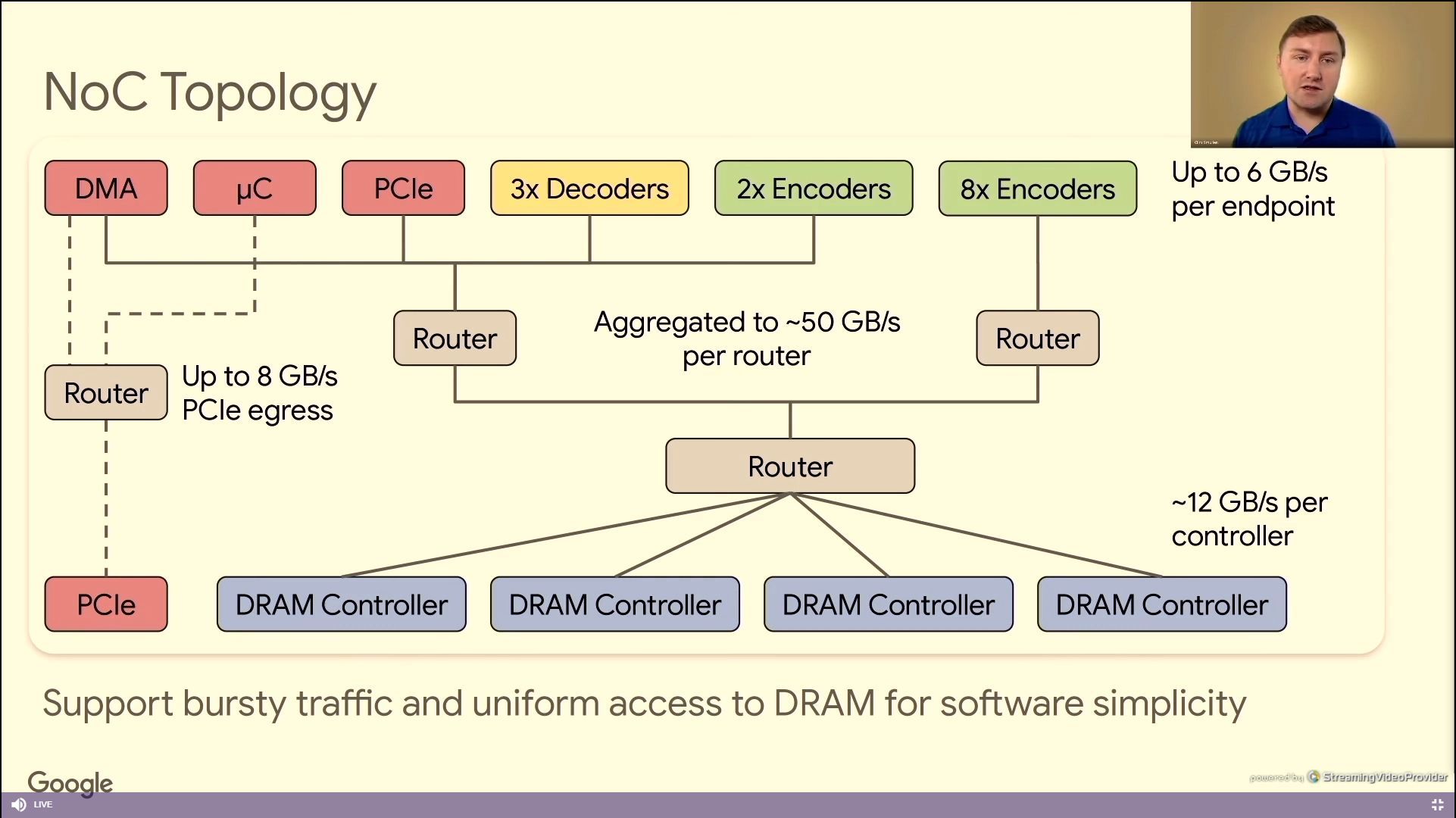
06:42PM EDT - conservative NOC design
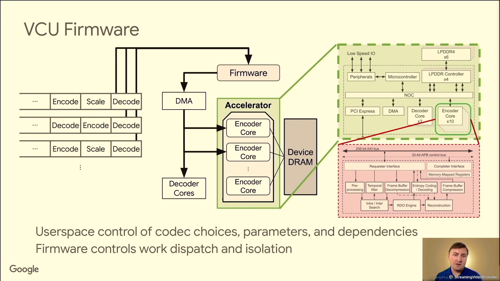
06:43PM EDT - A single decoded frame can be used multiple times - one decode for multiple encodes
06:43PM EDT - parallel queues for high utilization
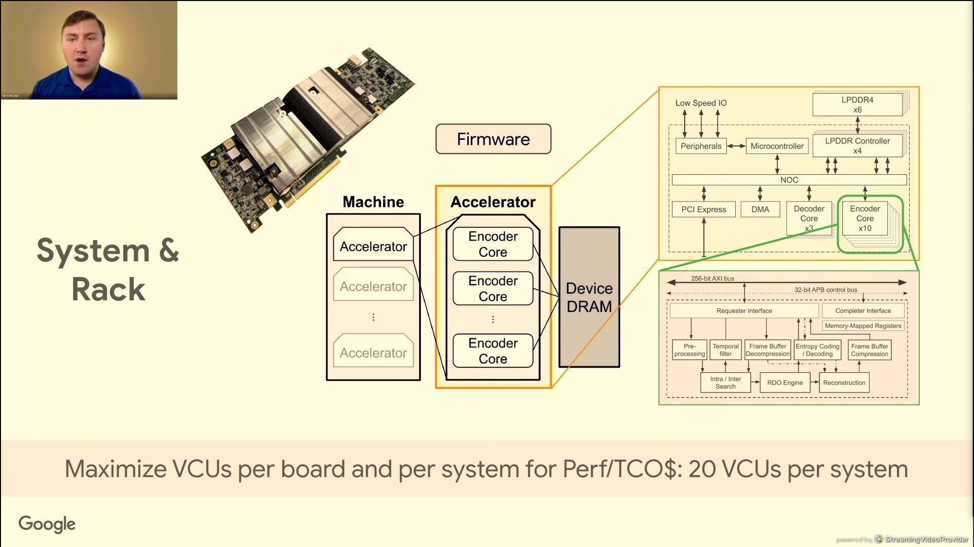
06:44PM EDT - 2 ASICs per board bifurcated, 5 boards per chassis, 2 chassis per host
06:44PM EDT - As many machines per rack as space and power allow
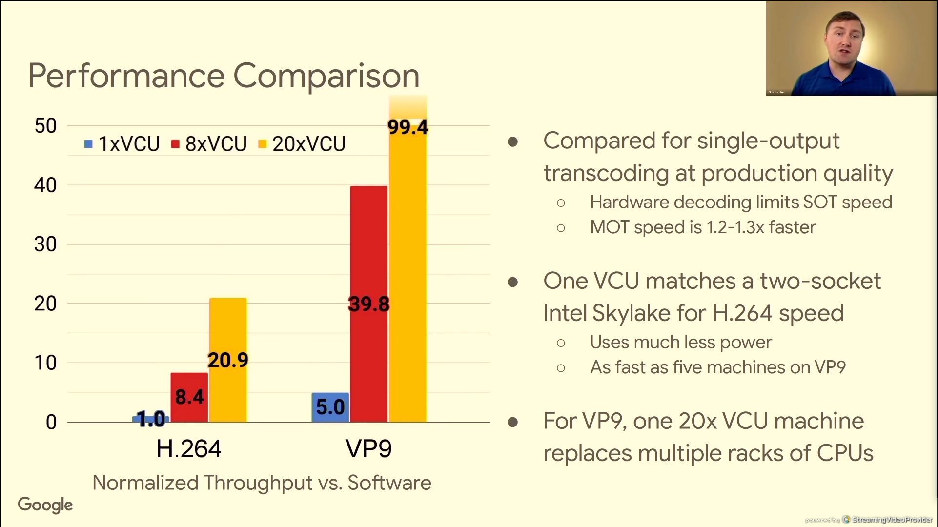
06:44PM EDT - Performance vs dual socket Skylake
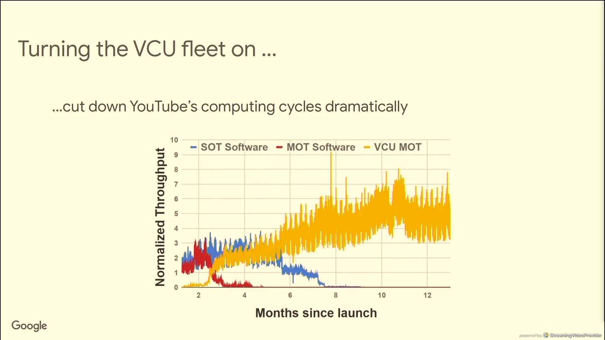
06:44PM EDT - 100x VP9 vs H.264
06:45PM EDT - one 20 VCU machine replaces racks of CPUs
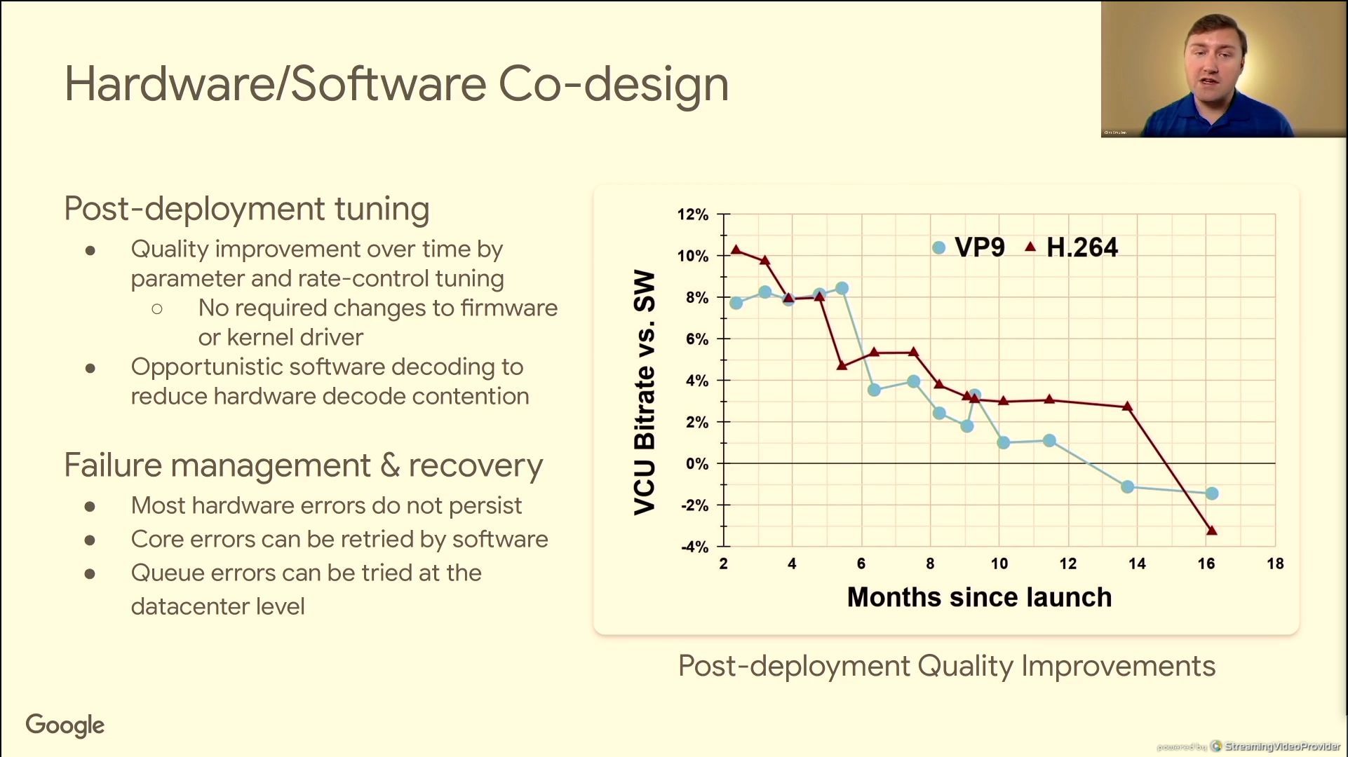
06:46PM EDT - Post-deployment improved quality
06:47PM EDT - Q&A time
06:49PM EDT - Q: Can VCU be in tandem with ASIC? A: Not possible, no intermediate tap in/tap out. Tightly coupled design
06:50PM EDT - Q: What is the PCIe card profile - lanes/TDP? A: In house bifurcation format, otherwise FHFL dual-slot, post silicon under 100W
06:50PM EDT - Q: VCU enable by GCP? A: Always looking for unique GCP, but no announcements.
06:52PM EDT - Q: Q: Can HLS draw parity with RTL? A: Yes
06:54PM EDT - Q: SECDED ECC caches? A: where possible SECDED, some SRAMs in codec encoder only does detection - if error does occur, we can reset the job
06:54PM EDT - Q: 8K60 - Can a single VCU do that? A: Throughput, yes. But no VP9 profile.
06:55PM EDT - Q: Other codecs? A: No comment of future formats. Heavily involved in AV1 next gen AV2
06:55PM EDT - Q; Audio streams? A: Stream is broken between video/audio, could be broken up and processed elsewhere. VCU doesn't touch audio
06:58PM EDT - Final talk is Xilinx
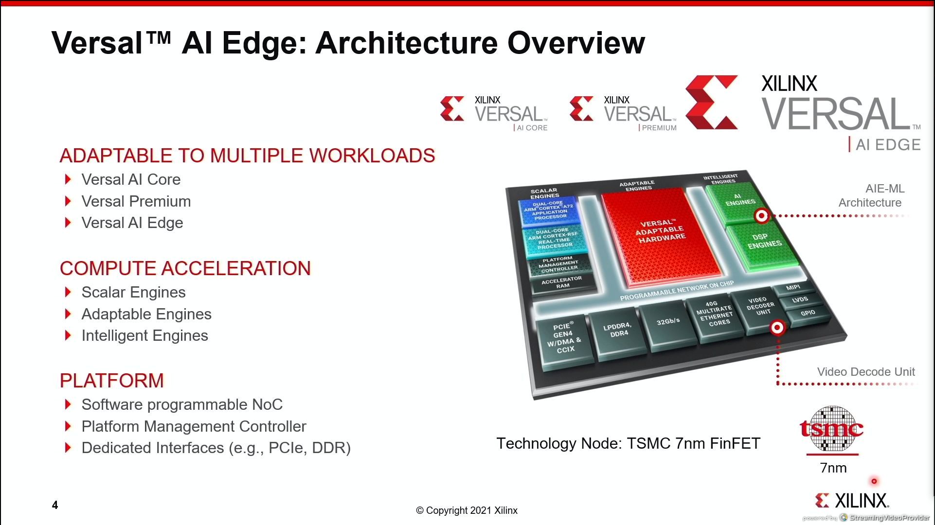
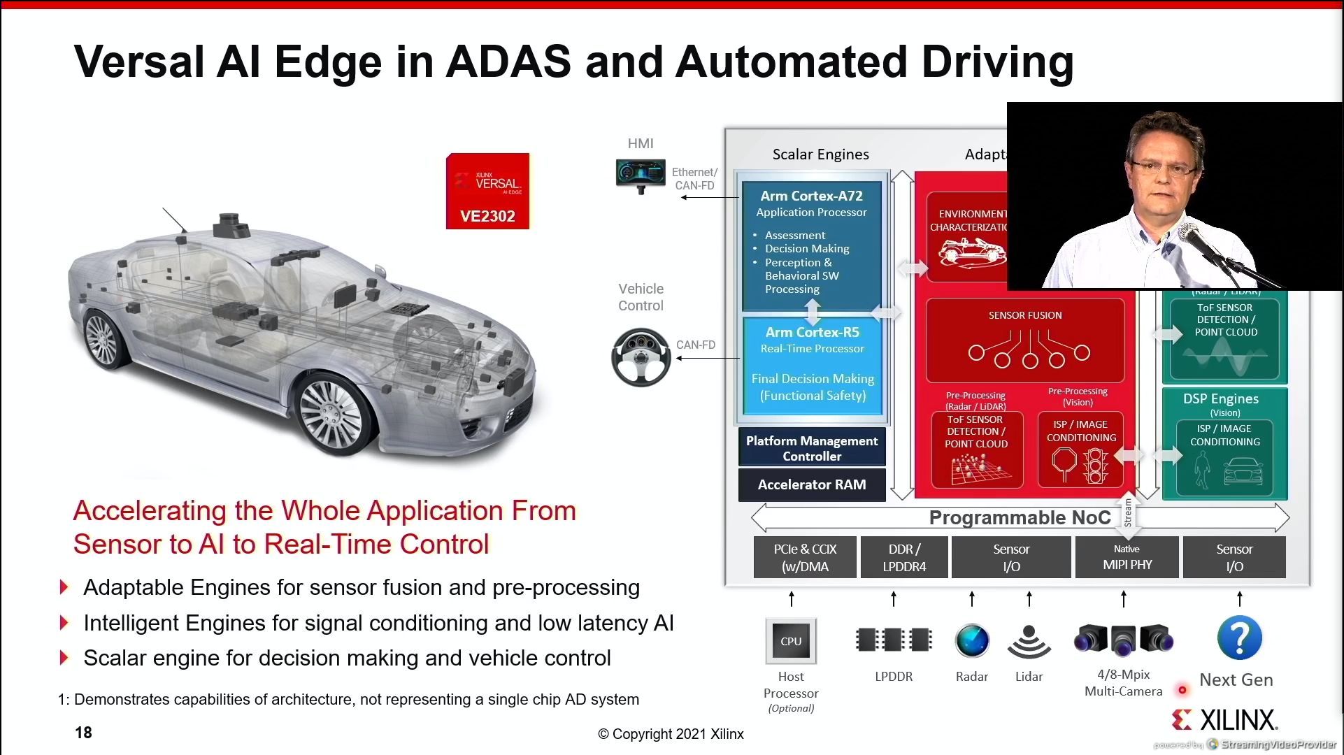
06:59PM EDT - Xilinx Versal AI Edge
06:59PM EDT - 7nm
06:59PM EDT - AIE-ML architecture optimized for inference
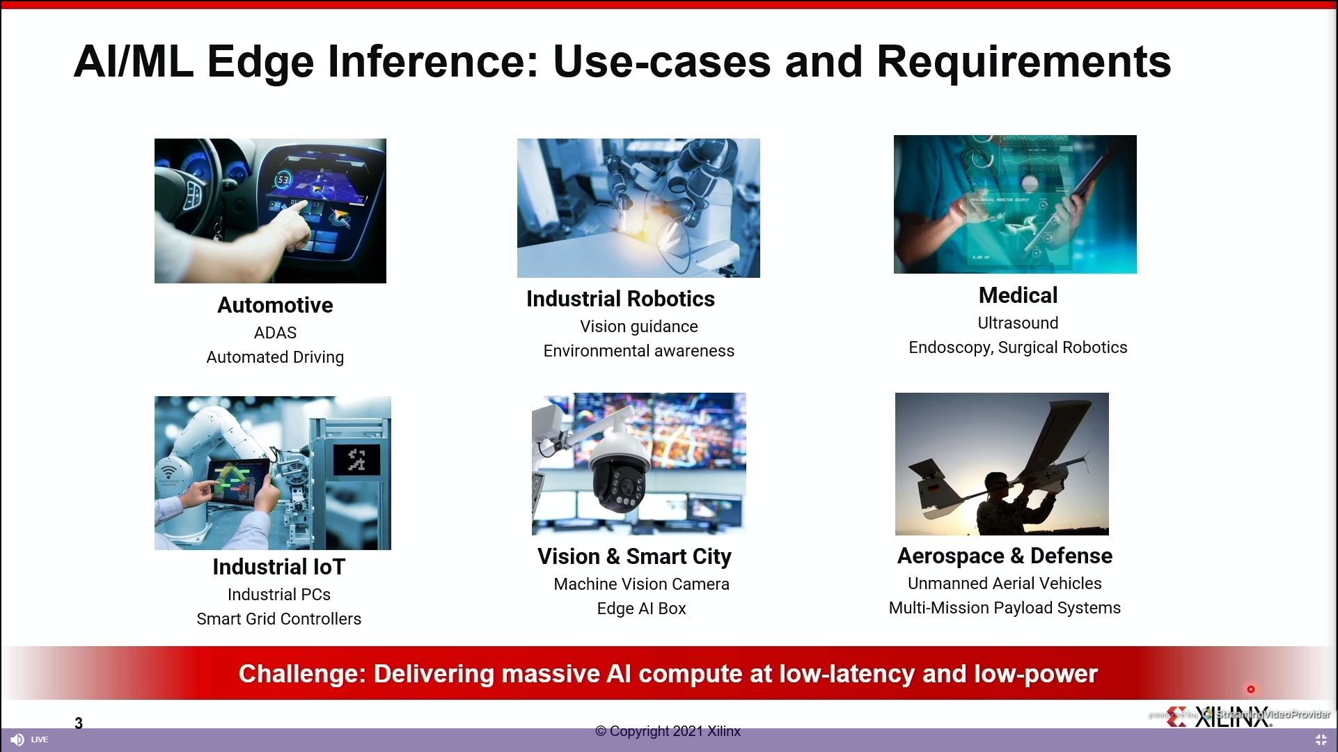
07:00PM EDT - What is ML used for
07:00PM EDT - All applications require lots of AI at low latency and low power
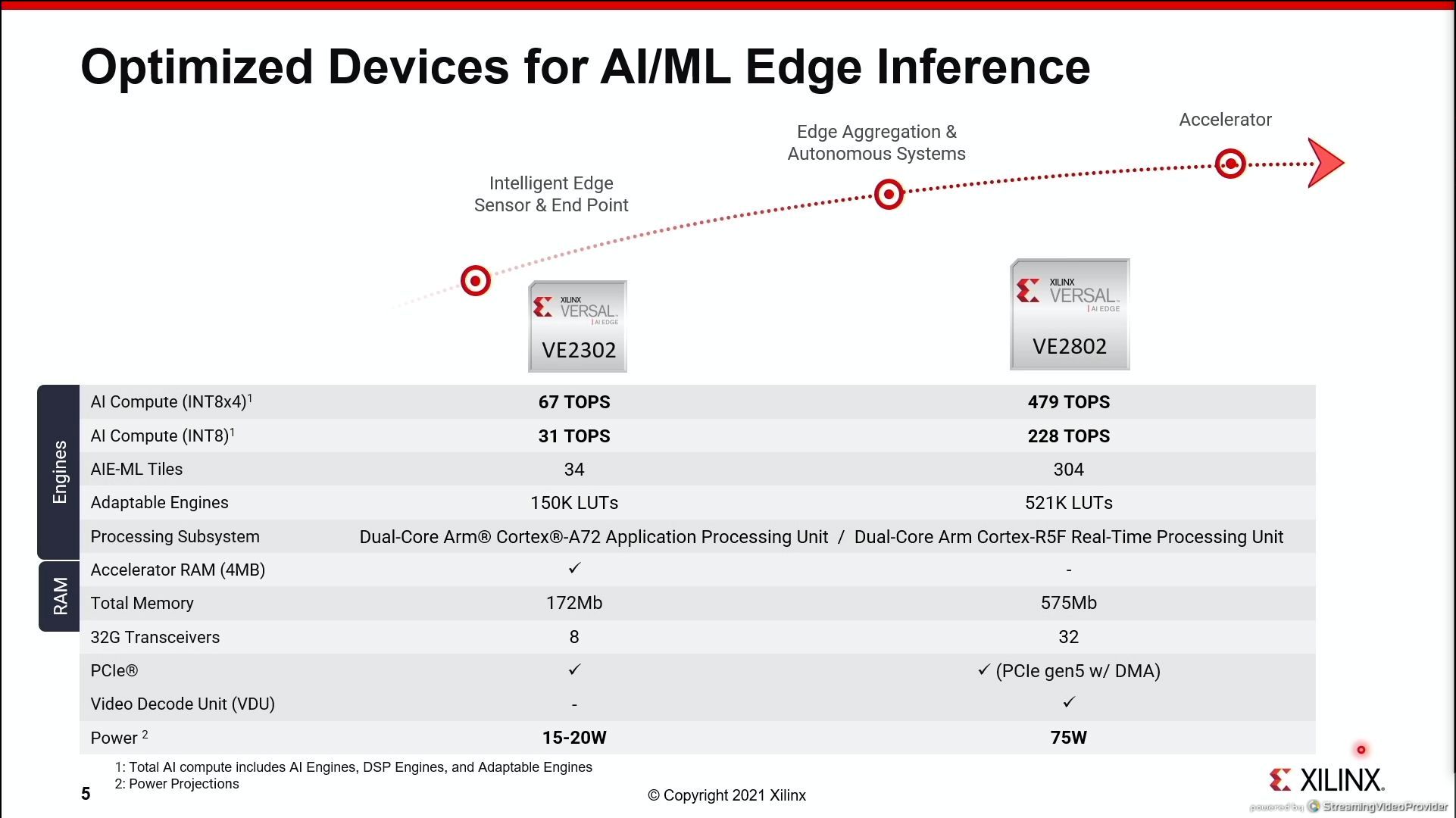
07:02PM EDT - low end and high end device highlighted today
07:03PM EDT - 10s of ML tiles to 100s of Tiles
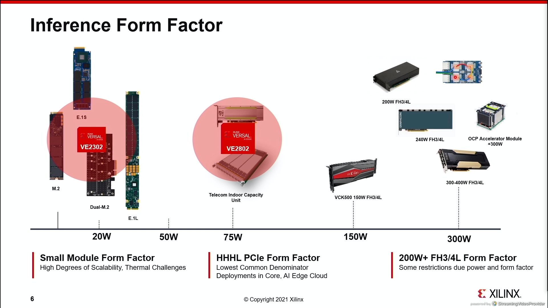
07:04PM EDT - lots of form factors for interece
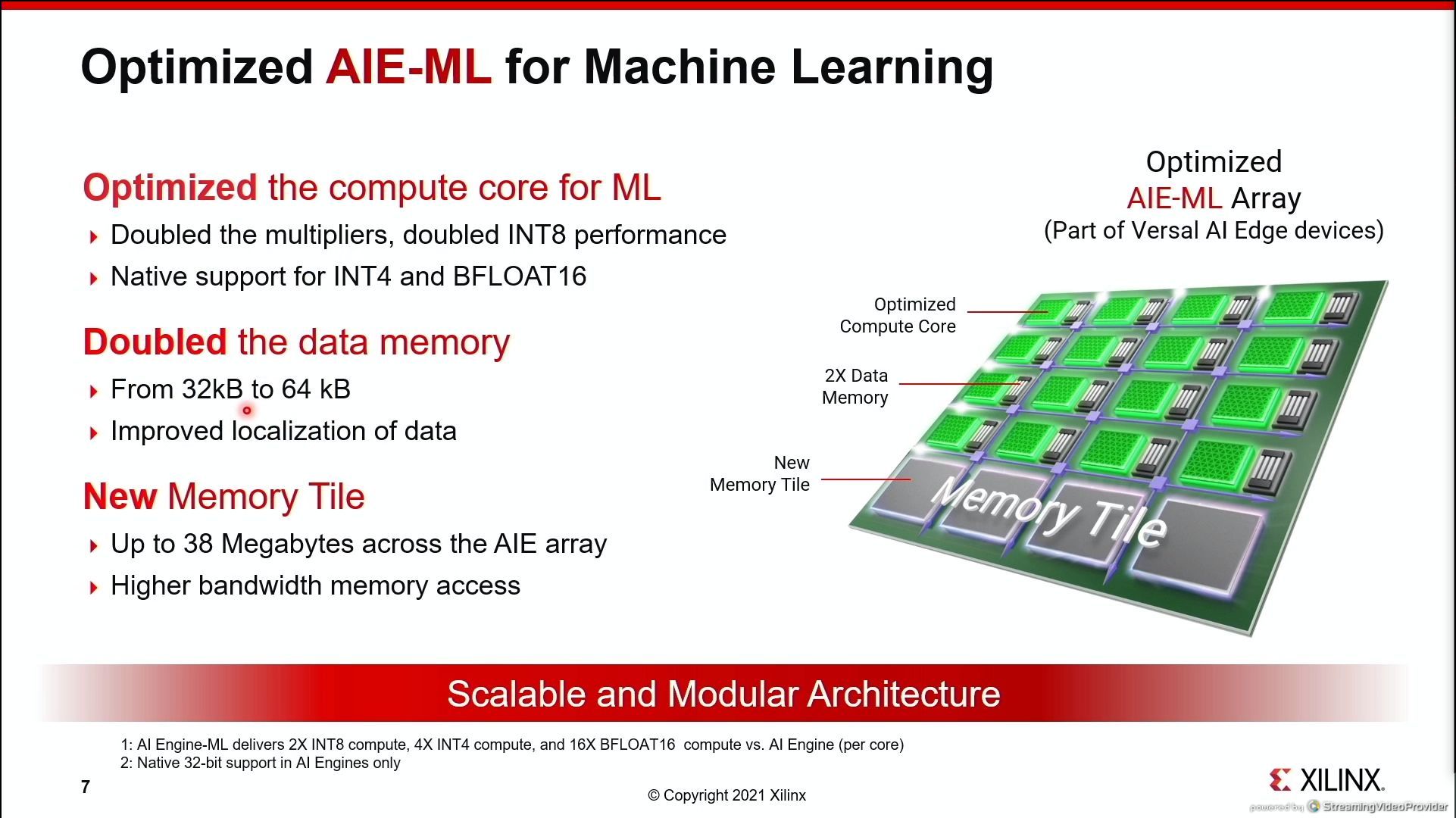
07:05PM EDT - Details on the Architecture
07:05PM EDT - memory tiles, optimized compute core
07:06PM EDT - Native support for INT4 and BF16
07:07PM EDT - SRAM is ECC protected
07:07PM EDT - Memory tile amount depends on device - mid-range is about 38 megabytes of memory tiles
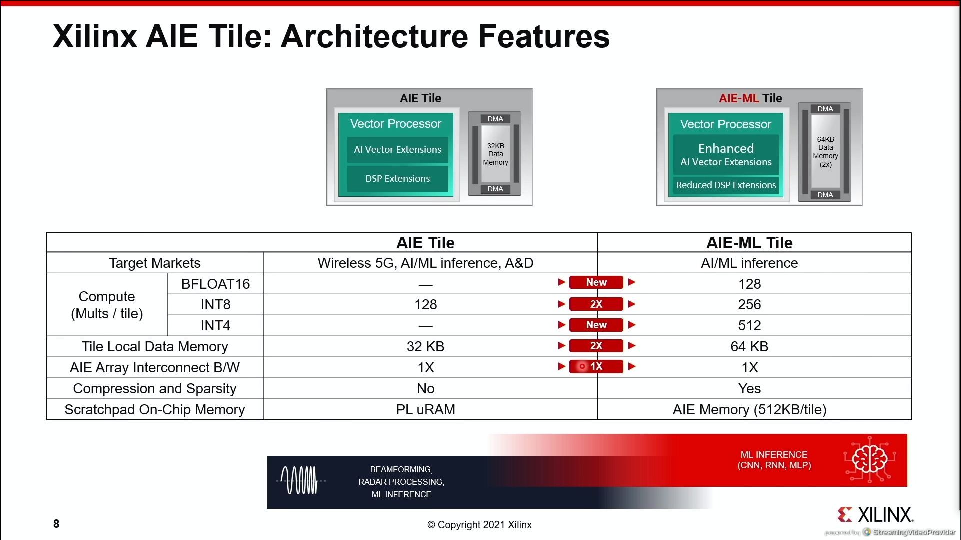
07:10PM EDT - New ML focused tile on these mid-range products
07:10PM EDT - high end still uses AIE because 5G needs it
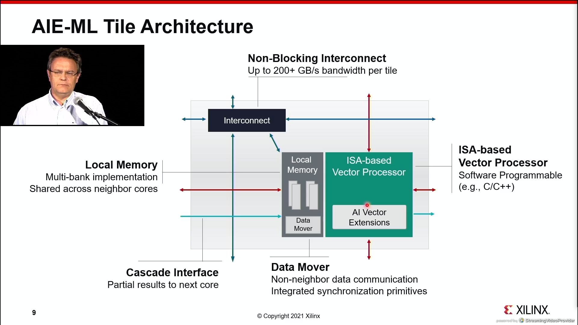
07:10PM EDT - VLIW vector processor
07:10PM EDT - non-blocking interconnect
07:10PM EDT - micro-DMA
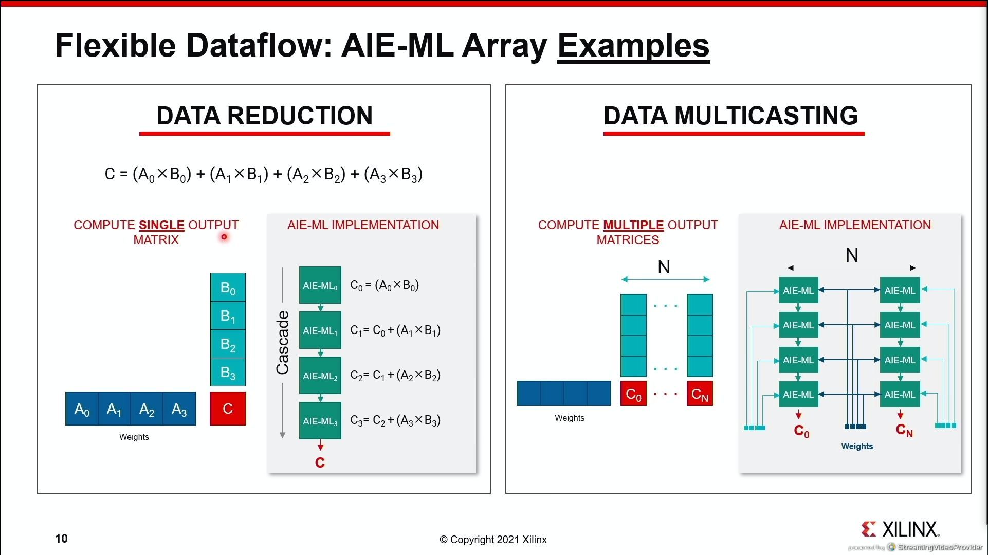

07:15PM EDT - device level data movement
07:15PM EDT - Tiles can read direct from DDR, no need intermediate levels
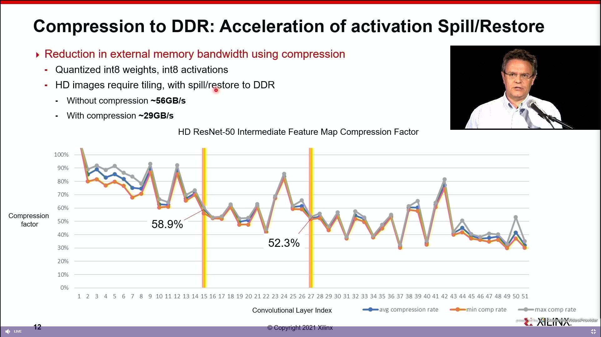
07:16PM EDT - DDR supports live compression
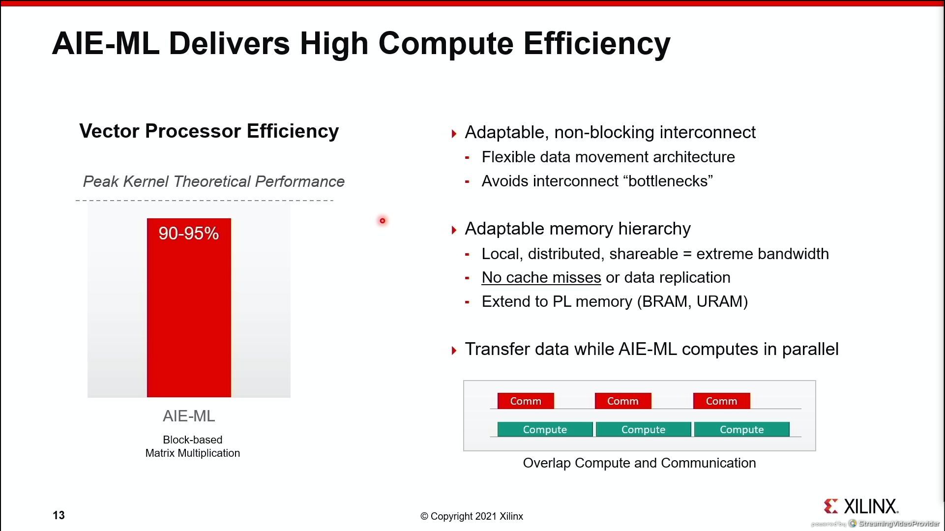
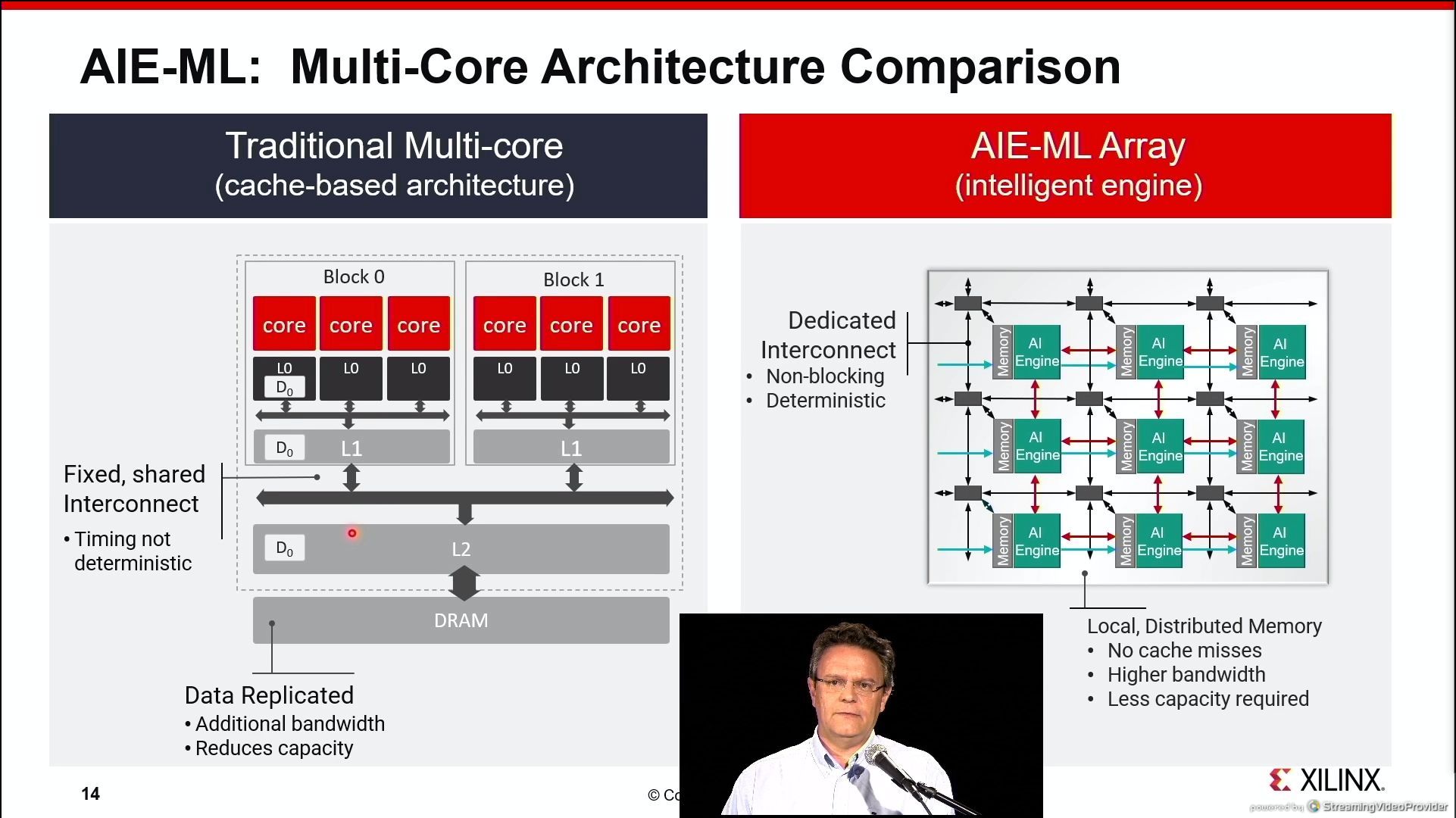
07:20PM EDT - memory is distributed, no data replication, no cache misses
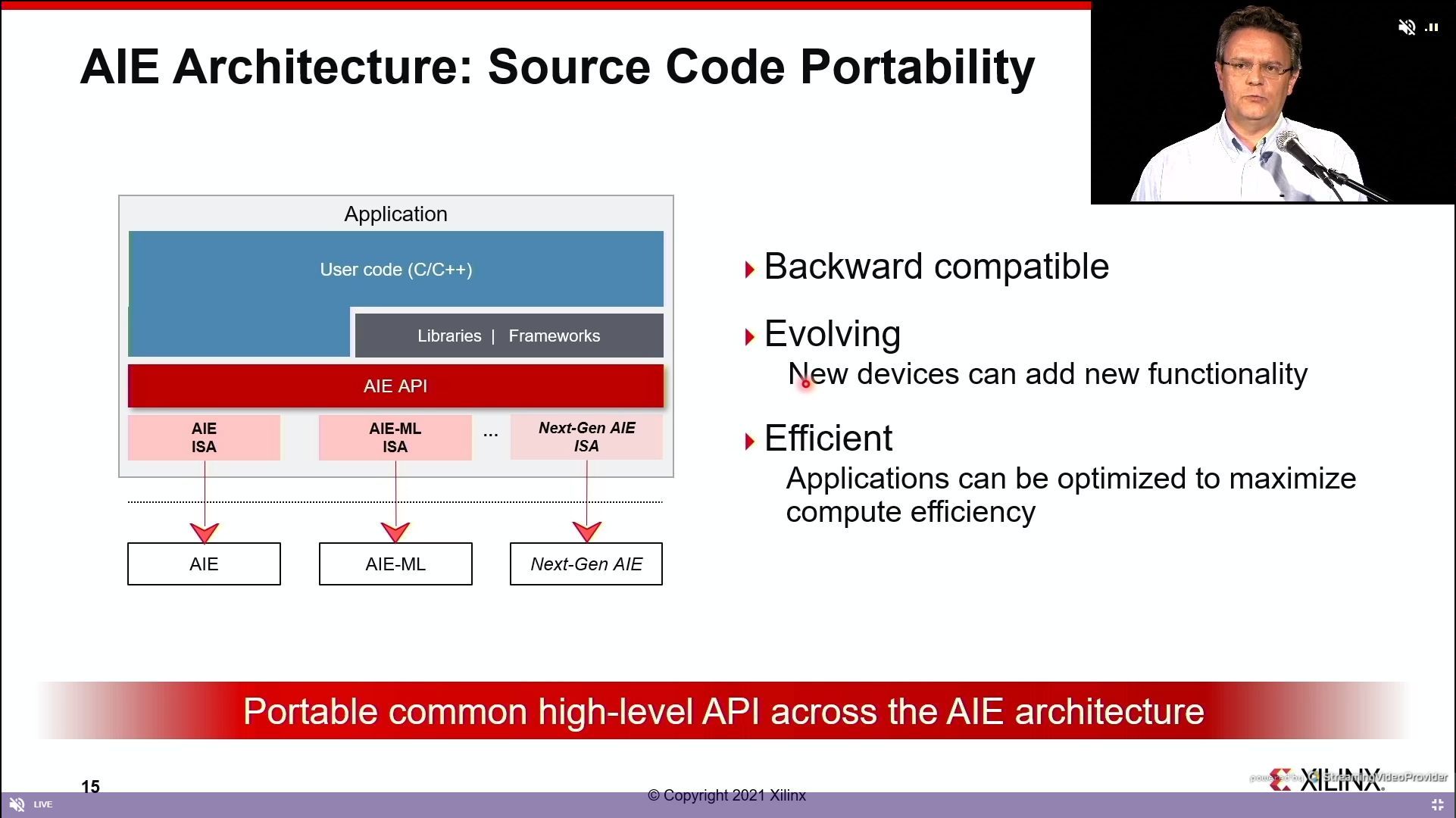
07:23PM EDT - COming soon to the software stack
07:23PM EDT - Don't need to program at C++ - pytorch, Tensorflow, Caffe, tvm
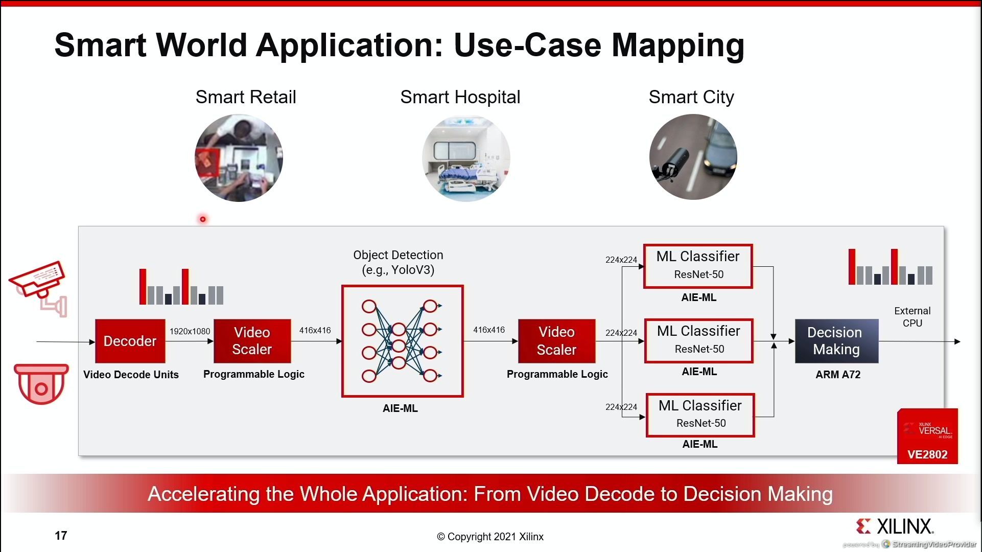
07:24PM EDT - use cases
07:25PM EDT - How to use a full Versal AI Edge processor for a single use

07:31PM EDT - That's a wrap


12 Comments
View All Comments
LuxZg - Thursday, August 26, 2021 - link
I'm lazy to search for article, but they are indeed developing new encoding hardware. But what was in the talk is just being deployed to their worldwide datacenters, well, may be close to finishing deployment by now, and they obviously want to boast about it. Similar how AMD talk was about current gen (boring right?) instead what's coming.First link I found right now:
https://min.news/en/tech/0144abd409e80e9edfdcc3aa4...
Quote: "some analysts believe that the technology giant could have replaced 33-40 million Intel CPUs with its own VCU"
Quote: "Google is already developing a second-generation VCU that supports AV1, H.264 and VP9 codecs because it needs to improve the efficiency of its encoding technology. It is not clear when Google will deploy the new VCU, but it is clear that the company wants to use its own processors as much as possible instead of general-purpose processors."
(story I read month or two ago went more in depth)
Zoomer - Tuesday, September 7, 2021 - link
It's pretty clear fixed function or more specialized processors will be much more efficient at 1 task than a GP CPU.