Does an AMD Chiplet Have a Core Count Limit?
by Dr. Ian Cutress on September 7, 2021 9:00 AM EST
When it was announced that AMD was set to give a presentation at Hot Chips on its newest Zen 3 microarchitecture, I was expecting the usual fare when a company goes through an already announced platform – a series of slides that we had seen before. In the Zen 3 presentation this was largely the case, except for one snippet of information that had not been disclosed before. This bit of info is quite important for considering AMD’s growth strategy.
In order to explain why this information was important, we have to talk about the different ways to connect two elements (like CPU cores, or full CPUs, or even GPUs) together.
Connectivity: Ring, Mesh, Crossbar, All-to-All
With two processing elements, the easiest way to connect them is by a direct connection. With three elements, similarly, each part can be directly connected to the other.
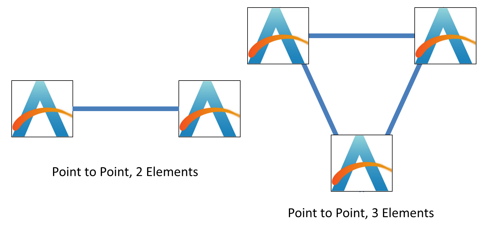
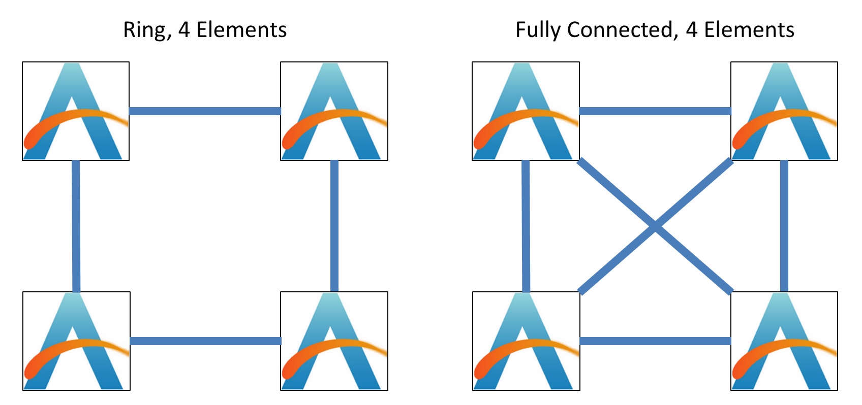
When we move up to four elements, options become available. The elements can either be similarly arranged in an all-to-all configuration, or into a ring.
The difference between the two comes down to latency, bandwidth, and power.
In the fully connected situation on the right, every element has a direct connection to each other, allowing for full connectivity bandwidth and the lowest latency. However, this comes with the tradeoff of power, given that each element has to have three connections. If we compare that to the ring, each element only has two connections, fixing the power, however because the average distance to each other element is no longer constant, and we have to pass data around the ring, it can cause variability in latency and bandwidth depending on what else is being sent around the ring.
Also with the ring, we have to consider if it can send data in one direction only, or in both directions.
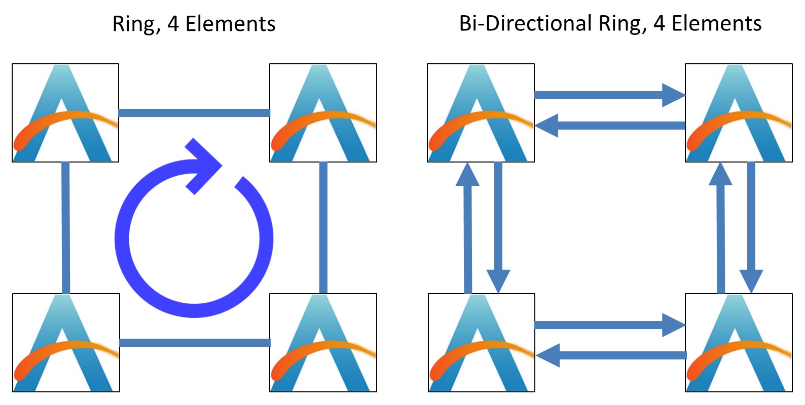
Almost all modern ring designs are bi-directional, allowing for data to flow in either direction. For the rest of this article, we’re assuming all rings are bi-directional. Some of the more modern Intel CPUs have double bi-directional rings, enabling for double bandwidth at the expense of double power, but one ring can be ‘turned off’ to save power in non-bandwidth limited scenarios.
The best way to consider the two four-element designs is through the number of connections and average hops to other elements:
- 4-Element Fully Connected: 3 Connections, 1 hop average
- 4-Element Bi-directional Ring: 2 Connections, 1.3 hop average
The same thing can occur with six-element configurations:
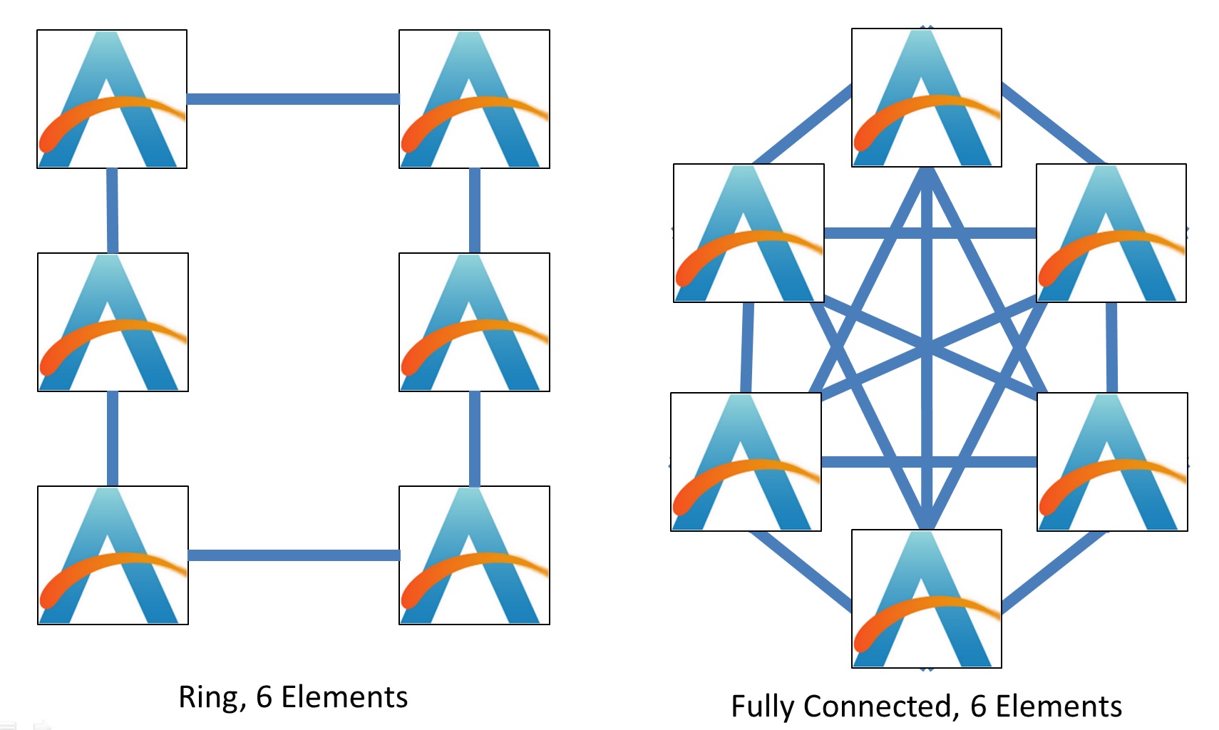
Here, the balance between bandwidth and power is more extreme. The ring design still relies on two connections per element, whereas a fully connected topology requires five connections per element. The fully connected design however remains at one hop average to access any other element, while the ring is now more complex at 1.8 hops per average access.
We can expand both somewhat indefinitely, however in modern CPU design, there is a substantial tradeoff in performance if increasing all of your power goes into maintaining those fully connected designs. There’s also one point to note here, we haven’t considered what else might be in the design – for example, modern Intel desktop CPUs, known for having rings, will also place the DRAM controllers, IO, and integrated graphics on the ring, so an 8-core design isn’t merely an 8-element ring:
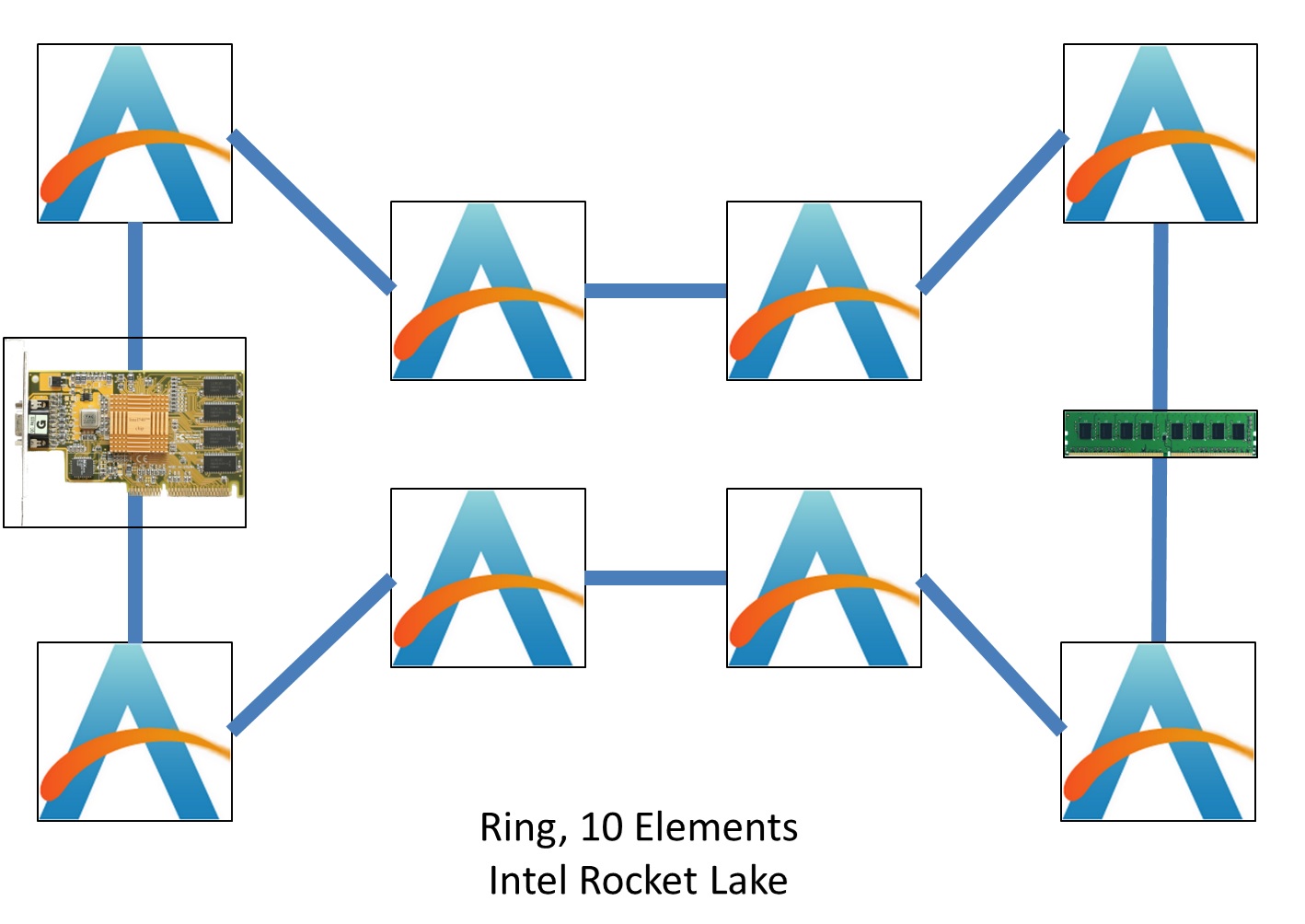
Here’s a simple mockup including the DRAM and integrated graphics. Truth be told, Intel doesn’t tell us everything about what’s connected to the ring, which means it can be difficult to determine where everything is located, however with synthetic tests we can see the average latency of a ring hop and try and go from there.
Intel has actually developed a way of connecting 8 elements together in not-a-ring but also not-fully-connected by giving each element the opportunity to have three connections. Again, the idea here is trading off some power for improved latency and bandwidth:
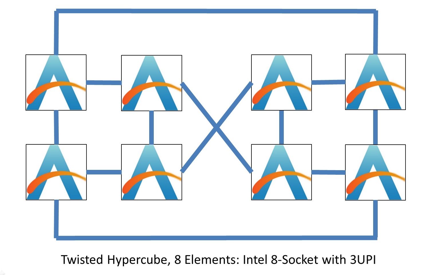
This is akin to taking the eight corners of a cube, creating rings on both sides, then implementing alternate connection strategies on the orthogonal faces. What it means is that each element is directly connected to three other elements, and everything else is two hops away:
- Twisted Hypercube, 8 Elements: 3 Connections, 1.57 average hops
In next-generation Sapphire Rapids, Intel is giving each CPU 4 connections, for 1.43 average hops.
Going above 10 elements in a ring, at least in modern core architectures, seems to be a bit of a problem due to the increased latency. You end up putting increasing stress on the ring as more cores usually means more bandwidth is needed to keep them all fed with data. Intel and other big-core single-chip AI companies have addressed this by implementing a two-dimensional mesh.
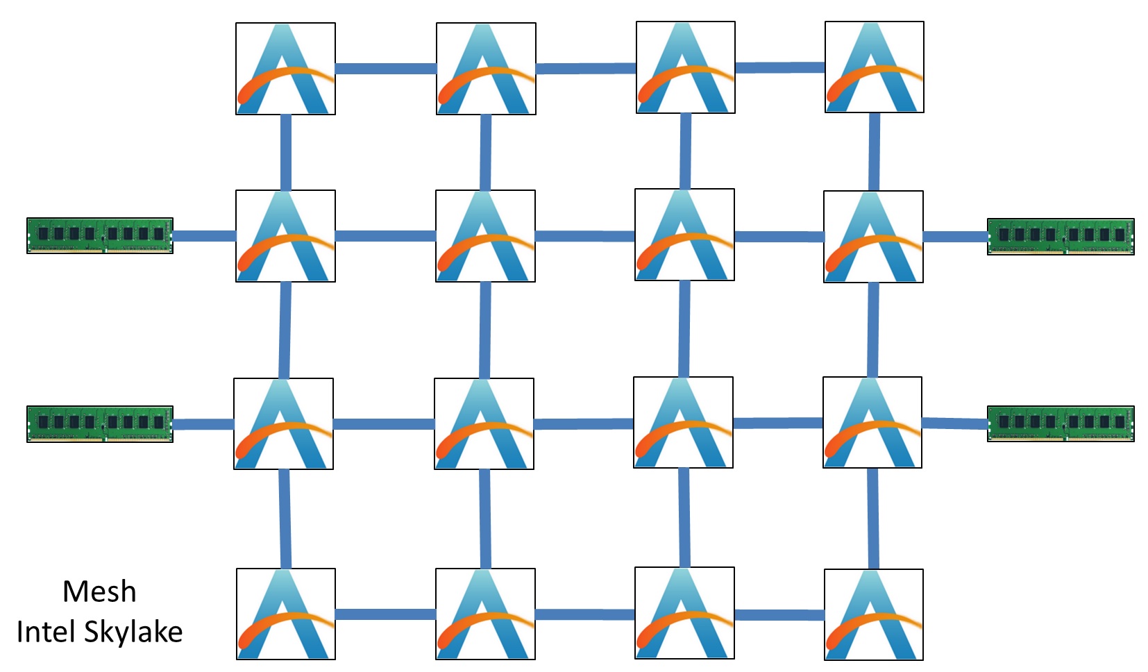
The mesh design trades off some additional per-element connections for better latency and connectivity. The average latency still varies, and in the event of data flow-heavy situations, data can take multiple routes to get to where it needs to go.
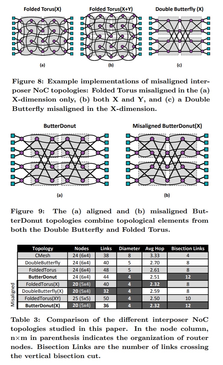
A 2D mesh is the simplest layout – each element next door is an x/y unit away. It revolves around each element being in a plane with no overlap of connectivity. There has been a lot of work done on topologies that take advantage of a little bit of 3D, which is where we might go to when chip-on-chip stacking technology is widely implemented. Here is an example paper of why a ButterDonut might be a good idea if mesh networks were implemented at the interposer level, as it minimizes hop links.
The other alternative is a Crossbar. The most basic view of a Crossbar is that it implements an effective all-to-all fully-connected topology for only a single connection. There are multiple types of crossbar, again depending on bandwidth, latency, and power requirements. A crossbar isn’t magical, what it really does is kick the connectivity problem one step down the road.
At this point of the article, we haven’t spoken how the elements are connected together. Inside a chip that usually means in silicon, however when we’re talking about connecting chips together, that might be through an interposer, or the PCB, which is more limiting in terms of how many high-speed connections it can hold and how many can crossover a given point. Often a physical external crossbar is needed to help simplify on-package connections, for example NVIDIA’s allows eight Tesla GPUs to connect in an all-to-all fashion by going through an NVSwitch, which is effectively a crossbar.
In this instance, here’s a diagram of a Switching Crossbar, which acts as a matrix or an internal mesh that manages where data needs to go.

In these sorts of environments, even though there is ‘only’ one connection to the crossbar compared to other configurations that might have two or three connections per element, consider that bandwidth might be double/triple to the crossbar than in a direct connection. This still means each element has more than one effective connection, and enjoys multiples of bandwidth if needed.
So Why Is AMD Limited?
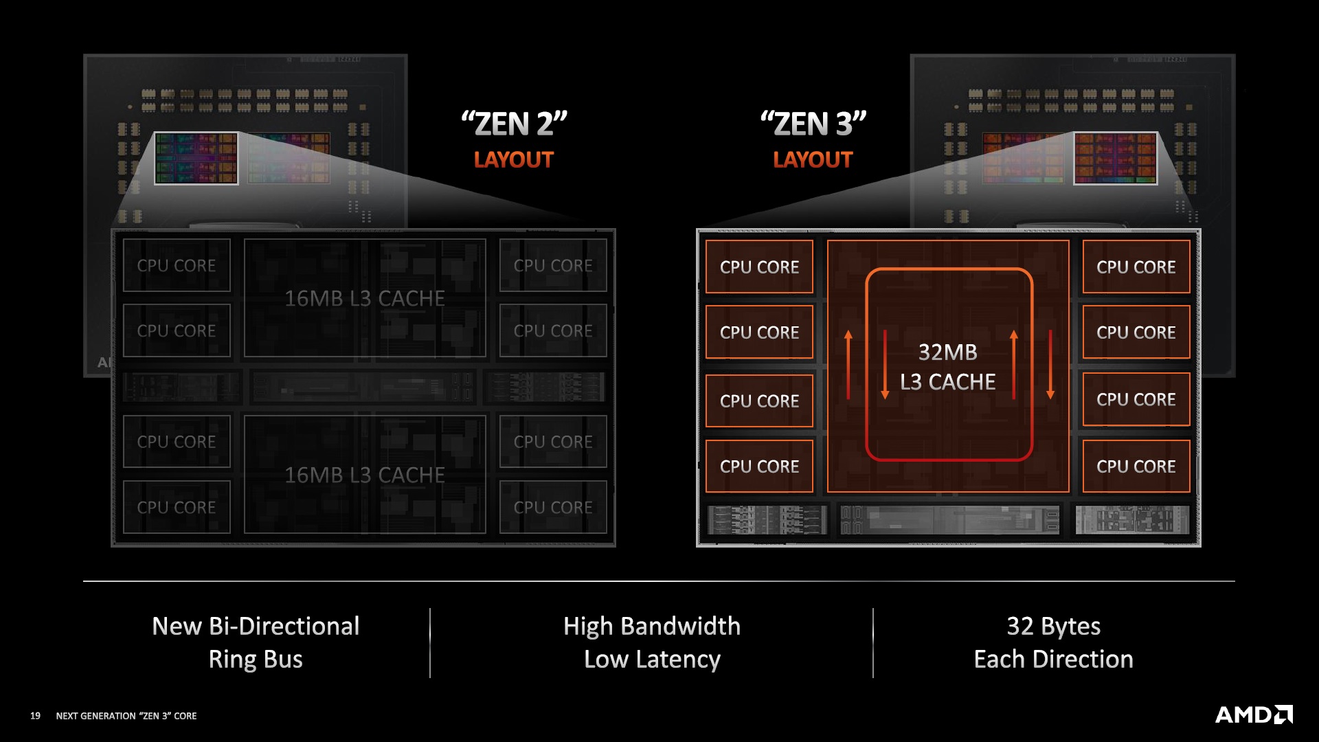
The reason for going through all of these explanations about connectivity is that when AMD moved from Zen 2 to Zen 3, it increased the number of cores inside a CCX (core complex). In Zen 2, a chiplet of eight cores had two four-core CCXes, and each of them connected to the main IO die, but with Zen 3, a single CCX grew to eight cores, and remained eight cores per chiplet.
When it was four cores per CCX, it was very easy to imagine (and test for) a fully-connected four-core topology. It isn’t that much extra to expect each core was connected to the other. Now with eight cores per CCX, since launch, AMD has been extremely coy about telling anyone publicly how those cores are connected together. When asked at launch if the cores in a Zen 3 eight-core CCX were fully connected, AMD’s general attitude was ‘Not quite, but close enough’. This would mean something between a ring and something between an all-to-all design, but more verging on the latter.
In our testing, we saw a similar CCX latency profile with eight cores as we had seen with four cores. This would essentially confirm AMD’s comments - we didn’t see any indication that AMD was using a ring. However, at Hot Chips, AMD’s Mark Evers (Chief Architect, Zen 3) presented this slide:
It was a bit of a shock to see it stated so clearly, given AMD’s apprehension in previous discussions about the topology. It was also a shock to have something new in this presentation, as pretty much everything else had been presented at previous events. However there are repercussions for this.
Going Beyond 8 Cores Per CCX
As AMD has been slowly increasing core counts on its processors, it has had two ways to do so: more chiplets or more cores per chiplet. With future generations of AMD processors expected to have more cores, it has to come from one of these two options. Both are viable, however it’s the more cores per chiplet option to consider.
We’ve spoken in this article about how rings trade off power and connections per element for latency and bandwidth, and how there can be an appreciable limit to how many elements or cores that can be put into a ring before the ring is the limiting factor. Intel, for example, has processors with 10 cores that use double bandwidth rings, but the most number of cores it has ever put into a ring is 12, with the Broadwell Server line of processors that ended up using dual 12-core rings. Note that each ring has more than 12 ring stops, because of extra functionality.

Each ring here has 12 ring stops for cores, two for ring-to-ring connectivity, one for DRAM, and the left ring has two extra stops for chip-to-chip and PCIe. That ring on the right has effectively 17 ring stops / elements attached to it. After this, Intel went to meshes.
Apply this scenario to AMD: if AMD were to grow the number of cores per CCX from eight in Zen 3, the most obvious answers are to either 12 cores or 16 cores. On a ring, neither of these two sound that appetizing.
AMD’s alternative to increasing cores on a chiplet is to simply double the number of CCXes. As with Zen 2, which had two lots of four cores, a future product could instead have two lots of eight cores, which would be an easy jump to a sixteen-core chiplet.
It is worth noting that AMD’s next-generation server platform, Genoa, is expected to have more than the 64 cores that AMD’s current generation has. Those 64 cores are eight chiplets of eight cores each, with one eight-core CCX per chiplet. Leaks have suggested that Genoa simply adds more chiplets, however that strategy isn’t infinitely scalable.
Moreover to all of this, consider AMD’s IO die in EPYC. It’s effectively a crossbar, right? All the chiplets come together to be connected, however AMD’s IO die is itself a Ring Crossbar design.
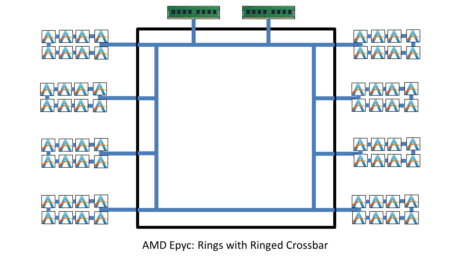
What we’ve ended up with from AMD is a ring of rings. In actual fact, the ring is a bit more complex:
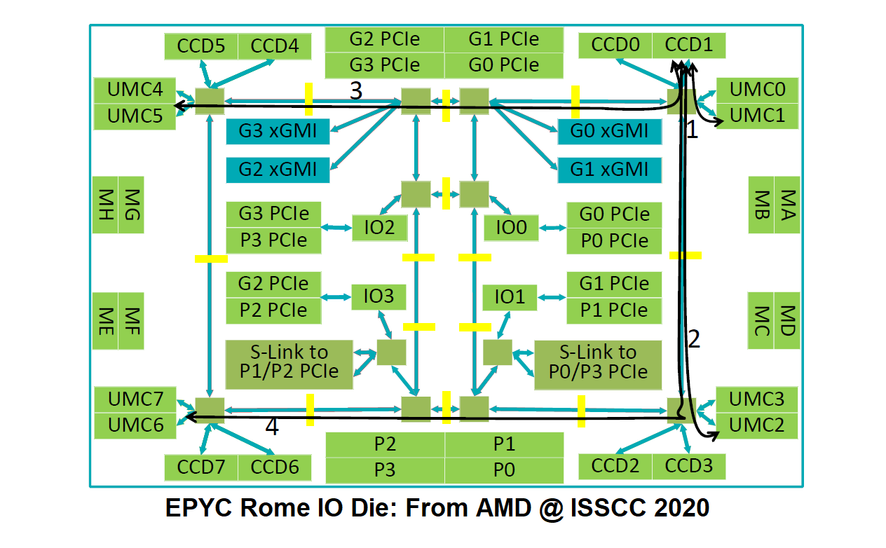
AMD’s IO die is one big outer ring with eight stops on it, and some of the stops have connections across the ring. It could be considered a mesh, or a bisected ring, and it looks something like this:
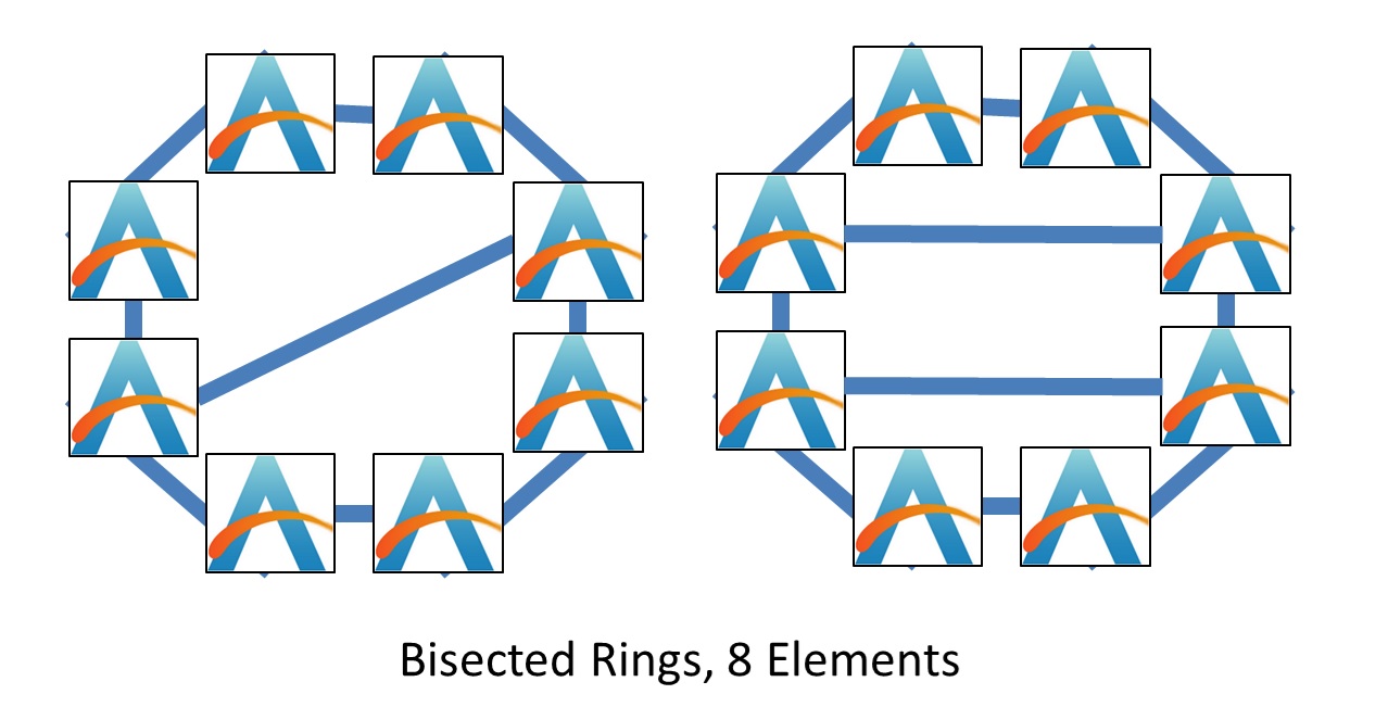
With a bisected ring, there’s now a non-uniform balance in the number of connections per element and the average latency – some elements have two connections, others have three. However, this is similar to the mesh in the sense that not every element has an identical bandwidth or latency profile. It is also important to note that a bisected ring can have one, two, or more internal connections.
So is AMD's Zen 3 8-Core CCX Really A Ring?
AMD tells us that its eight-core CCX structure is a bidirectional ring. If that’s the case, then AMD is going to struggle to move beyond eight cores per CCX. It could easily double cores per chiplet by simply doubling the number of CCXes, however beyond that the ring needs to change.
In our testing, our results show that while AMD’s core complex is not an all-to-all connection, it also doesn’t match what we would expect from ring latencies. Simply put, it’s got to be more than a ring. AMD has been very coy on the exact details of their CCX interconnect – by providing a slide saying it’s a ring reinforces the fact that it’s not an all-to-all interconnect, but we’re pretty sure it’s some form of a bisected ring, a detail that AMD has decided to leave out of the presentation.
Final Thoughts: Going Beyond Rings
As I have been writing this piece, it has occurred to me what might be in the future for this sort of design. In the x86-world, AMD has pioneered the 2D ‘CPU Chiplet’ without much IO, and AMD is moving forward with its vertical 3D stacking V-Cache technology as announced last year. As part of this article, I spoke about different sorts of mesh interconnect, and the fact that to do something innovative requires an interposer. Well, consider each CPU chiplet with another chiplet below, as an effective single-silicon interposer, solely for core-to-core interconnect.
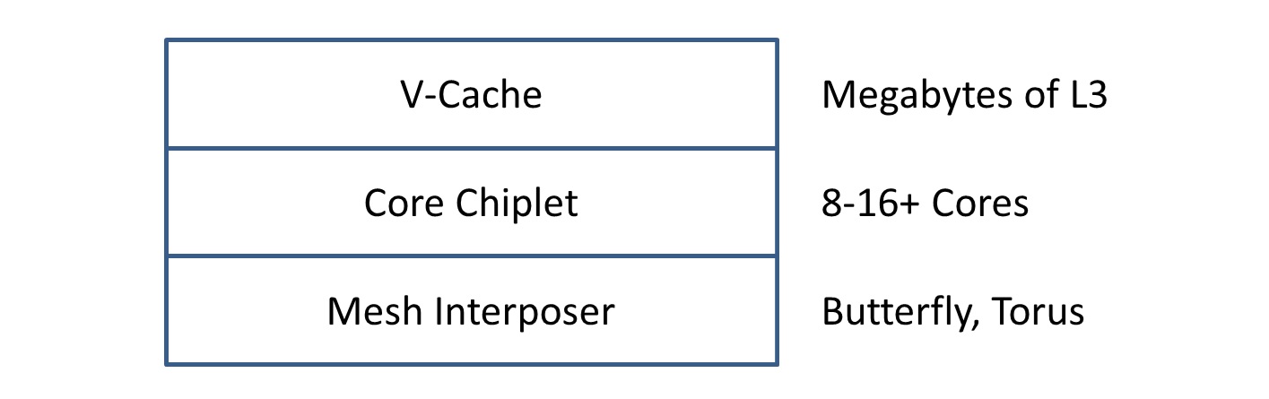
The interposer could be on a larger process node, e.g. 65nm, very high yielding, and move some of the logic away from the core chiplet, reducing its size or making more room for more innovation. The key here would be the vias required for data and power from the package, but AMD has extensive experience with its GPUs that require interposers.
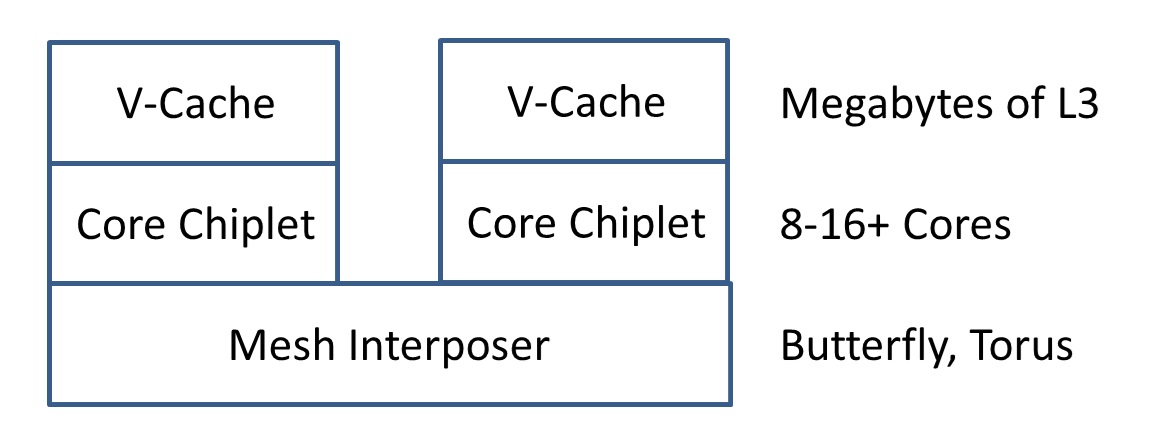
Alternatively, go one stage further – interposers are designed for multiple chiplets. If a 65nm high-yielding interposer is easy enough to make to fit two or three chiplets on, then just put multiple chiplets on there so they can act as one big chiplet with a unified cache between all of them. AMD has also stated that its V-Cache latency only increases with wire length, and so an interposer between two/three/four chiplets on either side of the IO die would not add significant latency to the cache.
The advent of chiplets and tiles means that as semiconductor companies start disaggregating their IP into separate bits of silicon, and packaging technologies get cheaper and higher-yielding, we’re going to see more innovation in areas that are starting to become bottlenecks, such as ring interconnects.


112 Comments
View All Comments
sweMike - Wednesday, September 8, 2021 - link
Well this article fails to mention several things. First the biggest advantage of going to chiplets is the increased performance and yield due to binning. Ie smaller chips has a lower chance of an error ruining the chip or degrading performance. Secondly one big avenue not mentioned is active interposers. Here they are portrayed as more or less passive. There are a lot of interesting possibilities with putting logic into the actual interposer. This article is pretty bad at covering this highly interesting are and focus on only one aspect and missing several key points. “AdoredTV” on YouTube has several videos covering this exact topic much better.Oxford Guy - Thursday, September 9, 2021 - link
‘There are a lot of interesting possibilities with putting logic into the actual interposer.’Article as I read it included that bit.
Ian Cutress - Sunday, September 12, 2021 - link
1) Chiplets. Oh dear god we've covered that 50-100 times on the site. It was assumed as given.2) Active interposers - did you not read the second half of the article? That's what this is _all_ about.
This comment is pretty bad at actually reading the content it's on.
Silver5urfer - Wednesday, September 8, 2021 - link
I could understand this piece a bit but its hard to get everything right. However that said there is a fundamental difference in AMD Ring vs Intel.AMD has an I/O die advantage over Intel. As Intel maxed out at 10C20T CML including all PCIe/iGPU/Memory. AMD maxes out at 16C32T because of the I/O die. That advantage is not there with Intel which is why their Mesh is garbage. It has significantly higher latency, power and lower performance when you add x86 core perf (IceLake) and AMD on the other hand relies on high cache. Just like Apple which also has high cache designs.
AMD cannot scale past 8C CCD on Zen 3 Ryzen or EPYC at the moment. On top seeing your old piece on 3D V Cache Hot Chips. Its clear that AMD is going to scale in 3D not 2D. That means they are going to stack the cores on top. Thermal issues are the first I could see there.
Finally Intel SPR is probably the first to scale to 14C28T scenario for mainstream. But Intel did not make it instead added crap cores and IDT to the equation on ADL because their dense 10nm / Intel 7 has insane power consumption again so they did not add real cores, now we will never know how fast Intel Ring is past Skylake designs look at RKL, utter failure literally ruined the core scaling, crap IMC, garbage TDP. On SPR they are again like Zen 1 NUMA and have no central I/O die which I said above. Intel cannot decouple the I/O from cores. AMD can which offers them superior flexibility. You should have mentioned that.
Genoa will scale I/O die if your theory is correct on AMD cannot scale beyond 8C CCD. Else we will see a 12C CCD shattering reality. A 12C CCD with high speed IF and Mem would be a beast in Mainstream AND Server/HEDT.
On Intel side new EMIB tile looks interesting but I want to see how it performs.
529th - Wednesday, September 8, 2021 - link
Do these topologies change even within a certain generation? e.g. 5600x vs a 5800x ? What's the 4 core version, btw?Thanks for the write up! Enjoyed the reading
abufrejoval - Wednesday, September 8, 2021 - link
The three layer variant with cache/cores/mesh really got stuck in my head, I believe it very credible.I'd love to see HBM or eDRAM variants to SRAM V-Cache, but I can easily imagine myself adding an S-RAM V-cache to my CPU basket soon.
For CCX variants, I'd also bet on 12-cores, but I am completely at loss on how this will play out on the "low-end".
After playing around with an 8-core 5800U based notebook at 15 Watts, I can't see myself paying even a penny for 12 cores. Above 40 Watts, sure, at 100 Watts yeah, but at 15 Watts: please wake me again tomorrow.
I've had 18 (Haswell) cores on one of my workstations for years, but the 8 cores of a Ryzen 5800X match it on all thready workloads.
I struggle to imagine reaping the benefit of having 128-512 x86 4GHz cores on my desktop workstations for the majority of my daily workloads with current software.
I've worked with CUDA ML workloads for years, which use 4K cores per socket and may scale to dozens of sockets. Their problems match these high core counts, even special architectures.
Excel (or databases) could put a CPU into every field and provide a real supercomputing calculus... but it doesn't, just like every little object in a browser's DOM won't do either.
On servers or with microservices, that matters much less, but for our workhorses aka workstations, I really see the worst of troubles ahead, because too few applications are able to exploit parallelism at these new levels.
By the time they might, hardware will have iterated several generations and then it's anyone's guess, where that might have lead...
Somehow I'd just much rather have Terahertz hardware or at leat memristors...
ShaftedByHaswell - Wednesday, September 8, 2021 - link
I do not understand why "three connections come with a power trade-off" with respect to "two connections".Is this concerning static power (i.e. leakage etc) or dynamic power?
Is this increase in power by using more connections not compensated by having less clock cycles needed to transfer the signal from one node to another node? I.e the trade off between more transistors active in one cycle versus less transistors active during more than one cycle?
Or are elements of these bus/mesh networks operating asynchronously, prof. Furber and Amulet being in mind?
The article is less than educational on how such a bus or mesh is constructed in terms of transistors.
JayNor - Wednesday, September 8, 2021 - link
"too few applications are able to exploit parallelism at these new levels"That seems to be rapidly addressed for any solution that demonstrates significant time savings.
Looks like the cpu memory controller bottleneck is now a problem for the large chips trying to do AI processing.
The Habana Gaudi architecture, with ROCE controller and 10x 100Gbe per package might be the way to go for CPUs and GPUs as well.
An interesting video discussed on reddit points to limitations in OS interrupt processing as a culprit, currently limiting processing when using the latest gen Optane SSDs. See the associated youtube video "More than 15 MILLION IOPs on Xeon 8380s: The State of IO 2021".
GeoffreyA - Wednesday, September 8, 2021 - link
Nice article, thank you. Well, it's midnight and I'm ready to hit the sack, so here's a mad scientist thought for the cores. Stack 'em in 4D, with a timelike separation, using hitherto unseen tech. Even better, let the cores stack with themselves. Only, the bi-directional links might be a bit of a problem: sending bits forward, no sweat; but backwards, might need a flux capacitor for that! And causality, oh, disaster ;)Dr_Mobeyos - Wednesday, September 8, 2021 - link
Haven't read the article yet, but just want to say thank you Anandtech. For the longest time I was trying to research NOC based crossbars, but public explanations online are scarce.