AMD Announces Instinct MI200 Accelerator Family: Taking Servers to Exascale and Beyond
by Ryan Smith on November 8, 2021 11:39 AM EST- Posted in
- GPUs
- AMD
- HPC
- AMD Instinct
- Infinity Fabric
- Exascale
- CDNA
- CDNA 2
Over the past half-decade, AMD has been slowly and steadily executing on a plan to reinvigorate the company. After reaching their lowest point in the middle of the 2010s, the company set out to become leaders in the processor space – to not just recapture lost glory, but to rise higher than the company ever has before. To reach that level of success, AMD would not only need to be competitive with traditional rivals Intel and NVIDIA in the consumer chip market, but break back into the true lifeblood of the processor industry: the server market.
Even more profitable than it is prestigious, a bustling server product lineup helps to keep a major processor designer like AMD well-rounded. Server parts aren’t sold in nearly the volume that consumer chips are, but the high margins for server parts more than offset their lower volume. And frequently, high-performance innovations designed for server chips will trickle down to consumer chips in some form. Having such a broad product portfolio has allowed Intel and NVIDIA to thrive over the years, and it’s something AMD needs as well for its long-term success.
On the CPU side of things, AMD is already firing on all cylinders. Its Zen 3 architecture has proven very potent, its chiplet strategy has allowed the company to balance production costs with scalability, and AMD’s server market share is greater than ever before, thanks to the success of AMD’s Milan processors. And while AMD isn’t letting their foot off of the gas pedal when it comes to CPUs, their immediate attention has switched to the other half of their product portfolio: GPUs.
Just as with their CPU architectures, AMD has spent the last several years building up their GPU architectures to be faster and more efficient – to be able to rival the best architectures from NVIDIA and others. And while the GPU business has gone about this in a slightly different fashion, by bifurcating GPU architectures into the RDNA and CDNA families, the overall plan of constant iteration remains unchanged. It’s a strategy that paid off handsomely for Milan, and now as we get ready to close out 2021, AMD is hoping to have their Milan moment in the GPU world.
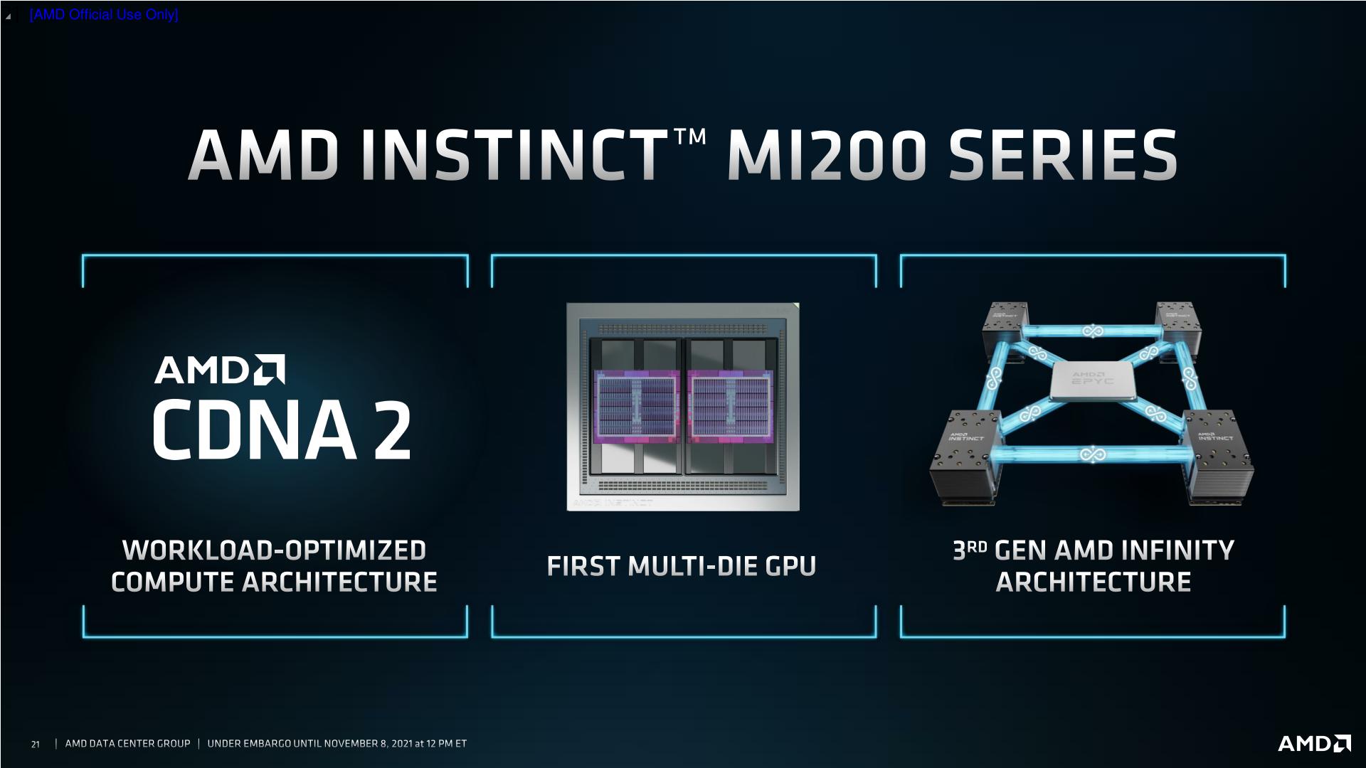
To that end, AMD today is formally unveiling their AMD Instinct MI200 family of server accelerators. Based on AMD’s new CDNA 2 architecture, the MI200 family is the capstone AMD’s server GPU plans for the last half-decade. By combing their GPU architectural experience with the latest manufacturing technology from TSMC and home-grown technologies such as their chip-to-chip Infinity Fabric, AMD has put together their most potent server GPUs yet. And with MI200 parts already shipping to the US Department of Energy as part of the Frontier exascale supercomputer contract, AMD is hoping that success will open up new avenues into the server market for the company.
The Heart of MI200: The CDNA2 Graphics Compute Die (GCD)
The release of the AMD Instinct MI200 series accelerators is in many respects the culmination of all of AMD’s efforts over the past several years. It’s not just the next step in their server GPU designs, but it’s where AMD begins to be able to fully leverage the synergies of being both a CPU provider and a GPU provider. By baking their Infinity Fabric links into both their server CPUs and their server GPUs, AMD now has the ability to offer a coherent memory space between its CPUs and GPUs, which for the right workload presents significant performance advantages.
We’ll dive into the architectural details of AMD’s new hardware in a bit, but at a high level, CDNA 2 is a direct evolution of CDNA (1), itself an evolution of AMD’s GCN architecture. While GCN was branched off into the RDNA architecture for consumer parts to better focus on graphical workloads, GCN and its descendants have always proven very capable at compute – especially when programmers take the time to optimize for the architecture. As a result, CDNA 2 doesn’t bring with it any massive changes over CDNA (1), but it does reinforce some of CDNA (1)’s weaknesses, as well as integrating the hardware needed to take full advantage of AMD’s Infinity Fabric.
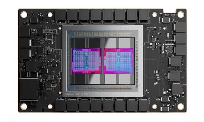
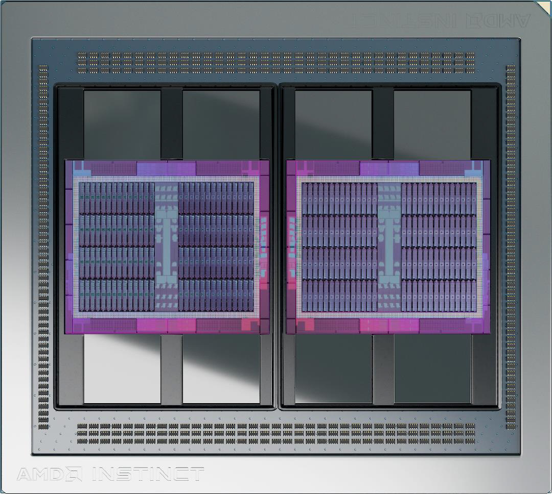
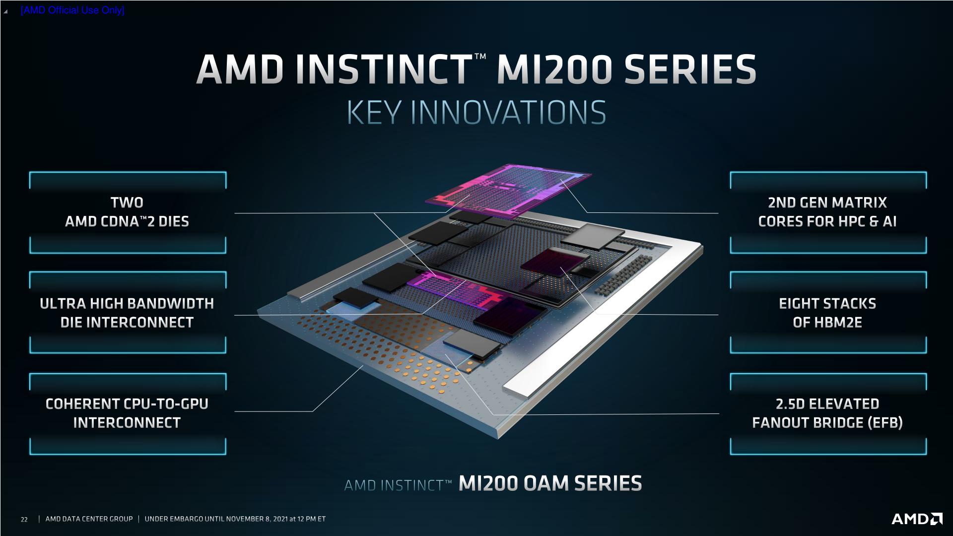
At the heart of AMD’s new products is the CDNA 2-based die. AMD hasn’t named it – or at least, isn’t sharing that name with us – but the company’s literature refers to it AMD Instinct MI200 Graphics Compute Die, or GCD. So for the sake of consistency, we’ll be referring to this sole CDNA 2 die as the GCD.
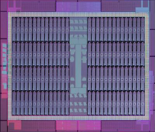
The GCD is a modest chip built on TSMC’s N6 process technology, making this the first AMD product built on that line. According to AMD each GCD is 29 billion transistors, and at least for the moment, AMD isn’t sharing anything about die sizes. As far as major functional blocks go, the GCD contains 112 CUs, which are organized into 4 Compute Engines. This is paired with 4 HBM2E memory controllers, and 8 Infinity Fabric Links.
On a generational basis, this is a relatively small increase in transistor count over the MI100 GPU. Despite doubling the number of off-die high-speed I/O links, as well as doubling the width of pretty much every last ALU on the die, the CDNA 2 GCD is only 14% (3.5B) transistors larger. Of course, this is tempered some by the overall reduction in CUs on a die, going from 120 in the last generation to 112 in CDNA 2. Still, AMD has clearly not spent too much of their savings from the move to TSMC N6 on adding too many more transistors to their design.
The upshot of a more modest transistor count and the smaller manufacturing process is that it opens the door to AMD embracing a chiplet-like design approach for their accelerators. As a result, the MI200 accelerators contain not one, but rather two GCDs in a multi-chip module (MCM) configuration. These two GPUs, in turn, are functionally independent of each other; but both are connected to the other via 4 Infinity Fabric links. This sets MI200 apart from previous AMD multi-GPU server offerings, as those products were all connected via the non-coherent PCIe bus.
This also means that, especially given the die-to-die coherency, AMD is quoting the full throughput of both GCDs for the performance of their MI200 accelerators. This is technically accurate in as much as the accelerators can, on paper, hit the quoted figures. But it still comes with caveats, as each MI200 accelerator is presented as two GPUs, and even as fast as 4 IF links are, moving data between GPUs is still much slower than within a single, monolithic GPU.
| AMD Instinct Accelerators | ||||||
| MI250X | MI250 | MI100 | MI50 | |||
| Compute Units | 2 x 110 | 2 x 10⁴ | 120 | 60 | ||
| Matrix Cores | 2 x 440 | 2 x 416 | 480 | N/A | ||
| Boost Clock | 1700MHz | 1700MHz | 1502MHz | 1725MHz | ||
| FP64 Vector | 47.9 TFLOPS | 45.3 TFLOPS | 11.5 TFLOPS | 6.6 TFLOPS | ||
| FP32 Vector | 47.9 TFLOPS | 45.3 TFLOPS | 23.1 TFLOPS | 13.3 TFLOPS | ||
| FP64 Matrix | 95.7 TFLOPS | 90.5 TFLOPS | 11.5 TFLOPS | 6.6 TFLOPS | ||
| FP32 Matrix | 95.7 TFLOPS | 90.5 TFLOPS | 46.1 TFLOPS | 13.3 TFLOPS | ||
| FP16 Matrix | 383 TFLOPS | 362 TFLOPS | 184.6 TFLOPS | 26.5 TFLOPS | ||
| INT8 Matrix | 383 TOPS | 362.1 TOPS | 184.6 TOPS | N/A | ||
| Memory Clock | 3.2 Gbps HBM2E | 3.2 Gbps HBM2E | 2.4 Gbps HBM2 | 2.0 Gbps GDDR6 | ||
| Memory Bus Width | 8192-bit | 8192-bit | 4096-bit | 4096-bit | ||
| Memory Bandwidth | 3.2TBps | 3.2TBps | 1.23TBps | 1.02TBps | ||
| VRAM | 128GB | 128GB | 32GB | 16GB | ||
| ECC | Yes (Full) | Yes (Full) | Yes (Full) | Yes (Full) | ||
| Infinity Fabric Links | 8 | 6 | 3 | N/A | ||
| CPU Coherency | Yes | No | N/A | N/A | ||
| TDP | 560W | 560W | 300W | 300W | ||
| Manufacturing Process | TSMC N6 | TSMC N6 | TSMC 7nm | TSMC 7nm | ||
| Transistor Count | 2 x 29.1B | 2 x 29.1B | 25.6B | 13.2B | ||
| Architecture | CDNA 2 | CDNA 2 | CDNA (1) | Vega | ||
| GPU | 2 x CDNA 2 GCD | 2 x CDNA 2 GCD | CDNA 1 | Vega 20 | ||
| Form Factor | OAM | OAM | PCIe | PCIe | ||
| Launch Date | 11/2021 | 11/2021 | 11/2020 | 11/2018 | ||
For today’s announcement, AMD is revealing 3 MI200 series accelerators. These are the top-end MI250X, it’s smaller sibling the MI250, and finally an MI200 PCIe card, the MI210. The two MI250 parts are the focus of today’s announcement, and for now AMD has not announced the full specifications of the MI210.
For AMD’s leading SKU, the MI250X comes with all features enabled, and as many active CUs as AMD can get away with. Its 220 CUs (110 per die) is just 4 short of a theoretical fully-enabled MI200 part. Breaking things down further, this works out to a total of 14,080 ALUs/Stream Processors between the two dies. Which, at a boost clock of 1.7GHz, works out to 47.9 TFLOPS of standard FP32 or FP64 vector throughput. For reference, this is more than double the FP32 throughput of the MI100, or more than four-times the FP64 throughput. Meanwhile, matrix/tensor throughput stands at 90.5 TFLOPS for FP64/32 operations, or 362.1 TFLOPS for FP16/BF16.
Following the MI250X we have the MI250. This part is very close in specifications to the MI250X, but drops a bit of performance and a few choice features. At its heart is 208 CUs (104 per chip), running with the same 1.7GHz boost clock. The shaves off about 5% of the processor’s performance versus the MI250X, a small amount in the big picture. Instead, what really sets the MI250 apart is that it only comes with 6 IF links, and it lacks coherency support. So customers who need that coherency support or every bit of chip-to-chip bandwidth that they can get will be pushed towards the MI250X instead.
Outside of those core differences, both parts are otherwise identical. Which on the memory front, means that the MI250 and MI250X both come with 8 stacks of HBM2E clocked at 3.2Gbps. Like every other aspect of these accelerators, those memory stacks are split between the two GCDs, so each GCD gets 4 stacks of memory. This gives each GCD about 1.64TB/second worth of memory bandwidth, or as AMD likes to promote it, a cumulative memory bandwidth of 3.2TB/second. Meanwhile ECC support is present throughout the chip, thanks to the combination of HBM2E’s native ECC support along with AMD baking it into the GCD’s pathways as well.
AMD is using 16GB HBM2E stacks here, which gives each GCD 64GB of memory, or a cumulative total of 128GB for the full package. For machine learning workloads this is a particularly big deal, as the largest models are (still) memory capacity bound.
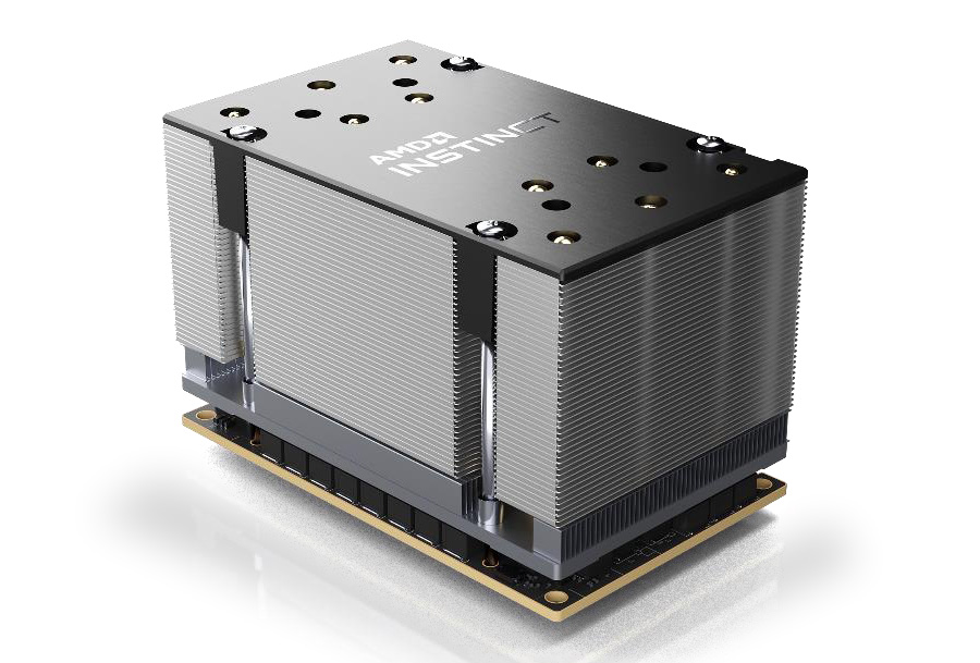
However all of this performance and memory comes at a cost: power consumption. To get the best performance out of the MI250(X) you’ll need to liquid cool it to handle its 560W TDP. Otherwise, the highest air-cooled configuration is still some 500W. Server accelerators requiring hundreds of watts is not uncommon, but at 500W+, it means that AMD has hit and passed the limits for air cooling a single accelerator. And AMD won’t be alone here; for top-end systems, we’re entering the era of liquid cooled servers.
Given that AMD is using two GPUs in an accelerator, such a high TDP is not all that surprising. But it does mean that a full, 8-way configuration – which is a supported configuration – will require upwards of 5000W just for the accelerators, never mind the rest of the system. AMD is very much playing in the big leagues in all respects here.
OCP Accelerator Module (OAM), Infinity Fabric 3.0, & Accelerator Topologies
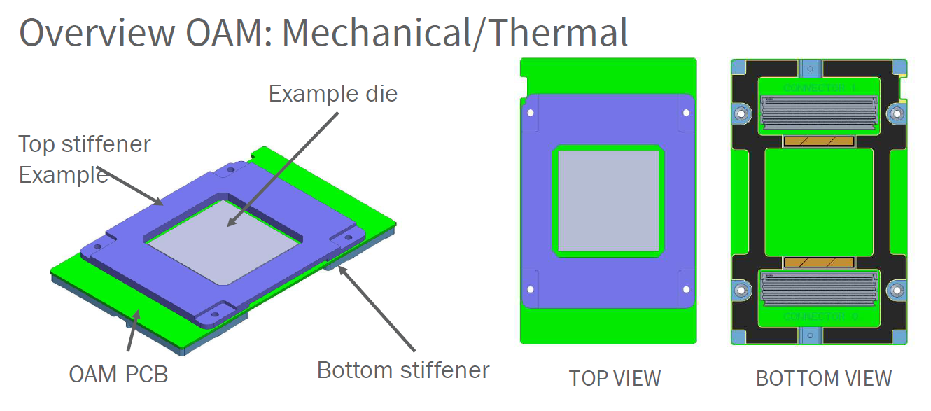
Along with AMD’s growing server ambitions also comes a change in hardware form factors to help fulfill those ambitions. For the MI250(X), AMD is using the Open Compute Project’s OCP Accelerator Module (OAM) form factor. This is a mezzanine-card style form factor that is not too dissimilar from NVIDIA’s SXM form factor. OAM has been around for a couple of years now and is designed particularly for GPUs and other types of accelerators, particularly those requiring a lot of bandwidth and a lot of power. Both AMD and Intel are among the first companies to publicly use OAM, with their respective accelerators using the form factor.
For the MI250(X), OAM is all but necessary to make full use of the platform. From a power and cooling standpoint, OAM is designed to scale much higher than dual-slot PCIe cards, with the spec maxing out at 700W for a single card. Meanwhile from an I/O standpoint, OAM has enough high-speed pins to enable eight 16-bit links, which is twice as many links as what AMD could do with a PCIe card. For similar reasons, it’s also a major component in enabling GPU/CPU coherency, as AMD needs the high-speed links to run IF from the GPUs to the CPUs.
Being a standardized interface, OAM also offers potential interoperability with other OAM hardware. Among the OCP’s projects is a universal baseboard design for OAM accelerators, which would allow server vendors and customers to use whatever type of accelerator is needed, be it AMD’s MI250(X), an in-house ML accelerator, or something else.
With the additional IF links exposed by the OAM form factor, AMD has given each GCD 8 Infinity Fabric 3.0 links. As previously mentioned, 4 of these links are used to couple the two GCDs within an MI200, which leaves 4 IF links per GCD (8 total) free for linking up to hosts and other accelerators.

All of these IF links are 16 bits wide an operate at 25Gbps/pin in a dual simplex fashion. This means there’s 50GB/second of bandwidth up and another 50GB/second of bandwidth down along each link. Or, as AMD likes to put it, each IF link is 100GB/second of bi-directional bandwidth, for a total aggregate bandwidth of 800GB/second. Notably, this gives the two GCDs within an MI250(X) 200GB/second of bandwidth in each direction to communicate among themselves. This is an immense amount of bandwidth, but for remote memory accesses it’s still going to be a fraction of the 1.6TB/second available to each GCD from its own HBM2E memory pool.
Otherwise, these links run at the same 25Gbps speed when going off-chip to other MI250s or an IF-equipped EPYC CPU. Besides the big benefit of coherency support when using IF, this is also 58% more bandwidth than what PCIe 4.0 would otherwise be capable of offering.
The 8 free IF links per package means that the MI250(X) can be installed into a number of different topologies. AMD’s favored topology, which is being used Frontier’s nodes, is a 4+1 setup with 4 accelerators attached to a single EPYC CPU via IF links, for a fully coherent setup. In this case each GCD has its own IF link to the CPU, and then there are 3 more links available to each GCD to connect with other GCDs. The net result is that it’s not a fully-connected setup – some GCDs will have to go through another GCD to reach any given GPU – but it accomplishes full coherency across all of the GPUs and with the CPU.
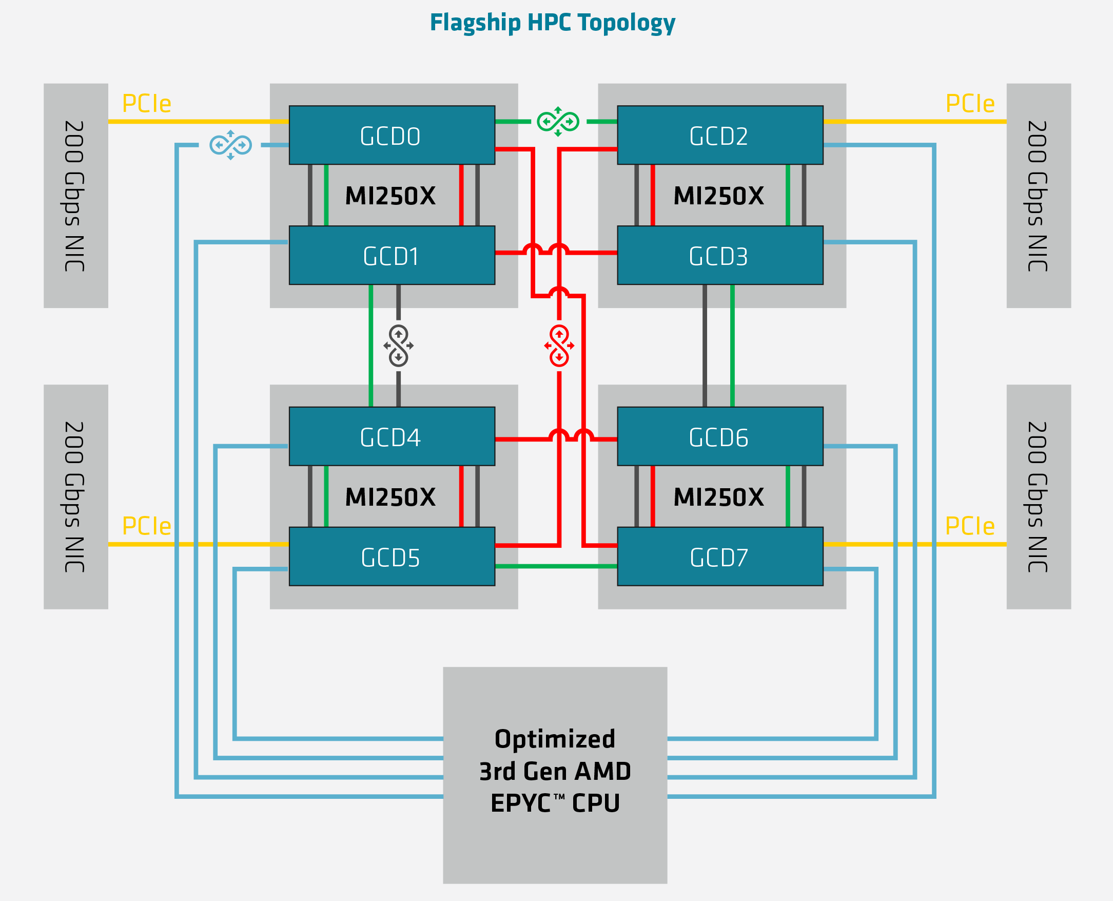
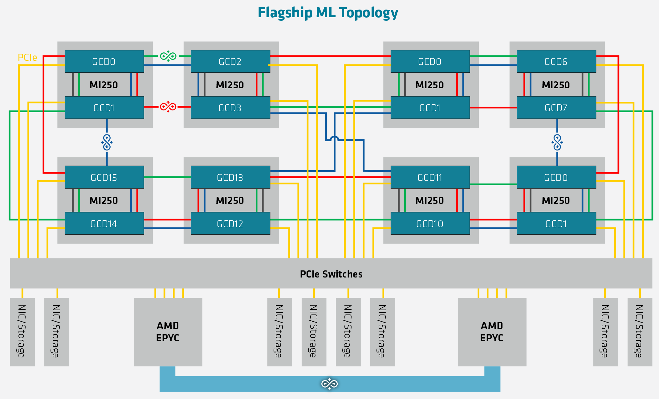
And while IF is clearly the most preferred method of communication, for customers who either can’t get or don’t need the special Epyc CPUs required, the master IF link in each GCD can also be used for PCIe communication. In which case the topology is the same, but each GPU is linked back to its host CPU by PCIe instead. And for the very adventurous ML server operators, it’s also possible to build an 8-way MI250(X) topology, which would result in 16 CDNA 2 GCDs inside a single system.


61 Comments
View All Comments
Matthias B V - Monday, November 8, 2021 - link
For me the most interesting is the information that they use N6 instead of N5.Usually those high price professional prroducts where the first to make use of new nodes... Really wonder what was the reason as performance and consumption should be much better. Yield and performance should be good!
- Not enough capacities? Don't think it is an issue as volumes for those cards are not that extreme.
Matthias B V - Monday, November 8, 2021 - link
I think it must be 3D Stacking for N5 as N7/N6 just got into mass production and they might not be ready to stack on N5 yet...yeeeeman - Monday, November 8, 2021 - link
apple is eating everything in the first few months.Matthias B V - Monday, November 8, 2021 - link
Yeah Apple was supposed to be masisve and first on N5 but N5 is a 2020 Node and we are talsking 2022...Fulljack - Monday, November 8, 2021 - link
Apple still sell their old 2020 device (iPhone, iPad, Mac family) that all has processor fabbed on TSMC N5. including this year's model, they'r still using a lot of TSMC N5 capacity.intelresting - Monday, November 8, 2021 - link
All the macbooks and probably coming macpros are N5Zoolook - Tuesday, November 9, 2021 - link
I saw a figure that Apple has 80% of N5 capacity reserved for 2021 and that was a while back.vlad42 - Monday, November 8, 2021 - link
Actually, the high priced professional products are typically one of the later product categories to use a new node. They high priced professional products are usually huge server CPUs, GPUs, or some other accelerator. Enterprises do not want to pay extra for the low yields of such large chips on new processes where the yields can still be significantly improved. The norm for a new node is typically cellphone SOCs > laptop/desktop CPUs/APUs/SOCs > consumer dGPUs > high performance professional products (servers/workstations) > embedded & networking chips.vlad42 - Monday, November 8, 2021 - link
Also, the big chips just take longer to design and optimize than the smaller chips.mode_13h - Monday, November 8, 2021 - link
Counterexample: A100 used TSMC N7, while Nvidia's consumer GPUs used Samsung's 8 nm.