The Snapdragon 8 Gen 1 Performance Preview: Sizing Up Cortex-X2
by Dr. Ian Cutress on December 14, 2021 8:00 AM EST
At the recent Qualcomm Snapdragon Tech Summit, the company announced its new flagship smartphone processor, the Snapdragon 8 Gen 1. Replacing the Snapdragon 888, this new chip is set to be in a number of high performance flagship smartphones in 2022. The new chip is Qualcomm’s first to use Arm v9 CPU cores as well as Samsung’s 4nm process node technology. In advance of devices coming in Q1, we attended a benchmarking session using Qualcomm’s reference design, and had a couple of hours to run tests focused on the new performance core, based on Arm’s Cortex-X2 core IP.
The Snapdragon 8 Gen 1
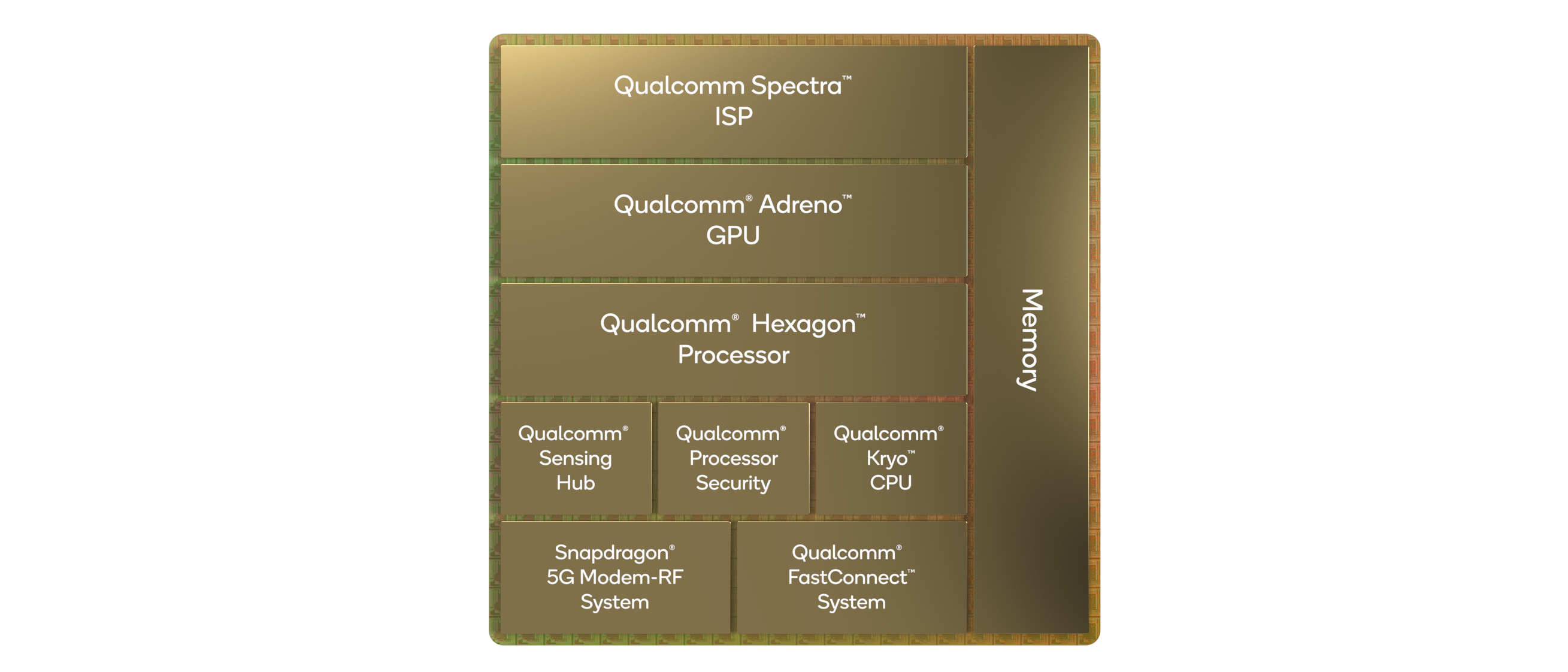
Rather than continue with the 800 naming scheme, Qualcomm is renaming its smartphone processor portfolio to make it easier to understand / market to consumers. The Snapdragon 8 Gen 1 (hereafter referred to as S8g1 or 8g1) will be the headliner for the portfolio, and we expect Qualcomm to announce other processors in the family as we move into 2022. The S8g1 uses the latest range of Arm core IP, along with updated Adreno, Hexagon, and connectivity IP including an integrated X65 modem capable of both mmWave and Sub 6 GHz for a worldwide solution in a single chip.
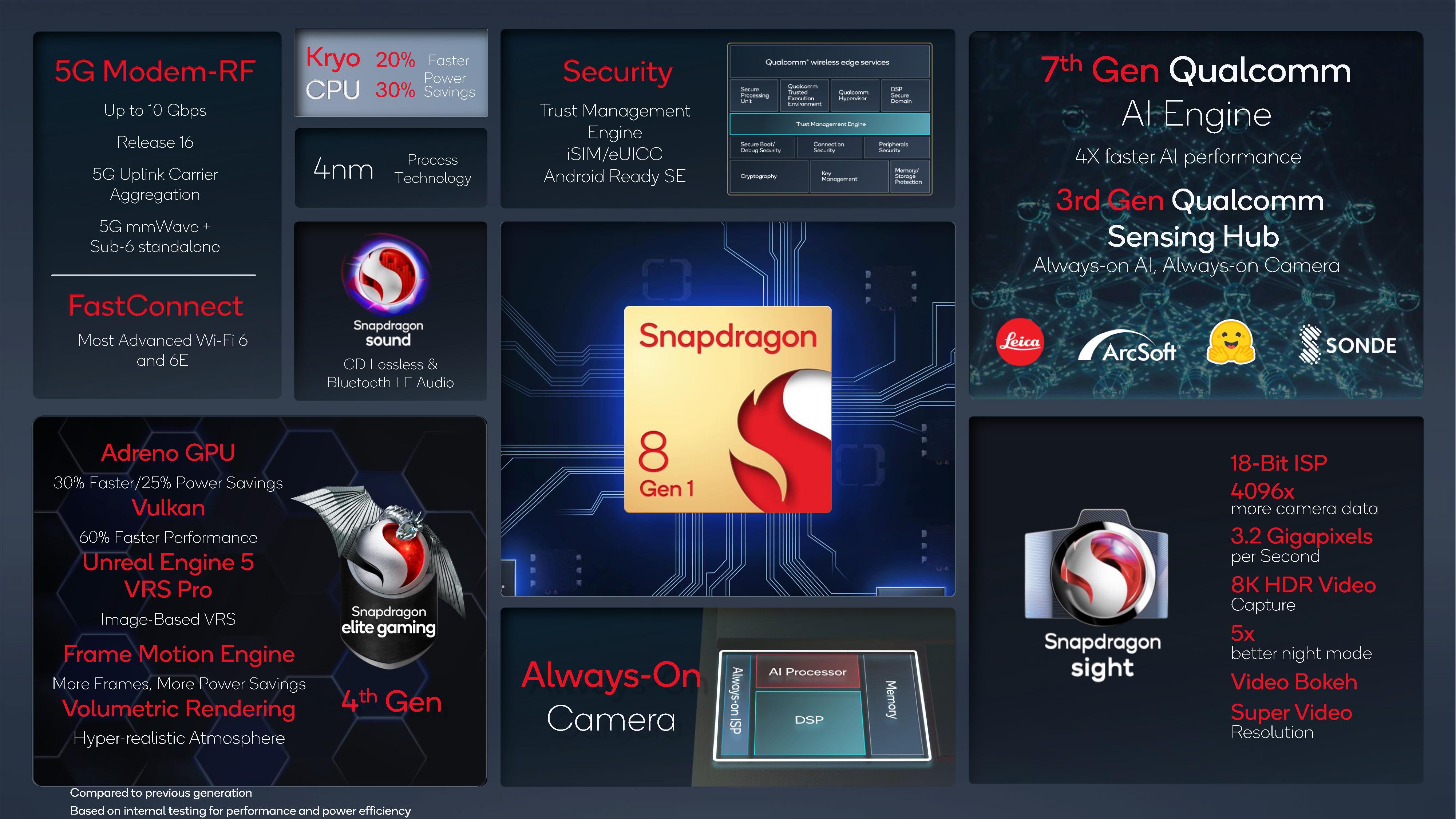
While Qualcomm hasn’t given any additional insight into the Adreno / graphics part of the hardware, not even giving us a 3-digit identifier, we have been told that it is a new ground up design. Qualcomm has also told us that the new GPU family is designed to look very similar to previous Adreno GPU sfrom a feature/API standpoint, which means that for existing games and other apps, it should allow a smooth transition with better performance. We had time to run a few traditional gaming tests in this piece.
On the DSP side, Qualcomm’s headlines are that the chip can process 3.2 Gigapixels/sec for the cameras with an 18-bit pipeline, suitable for a single 200MP camera, 64MP burst capture, or 8K HDR video. The encode/decode engines allow for 8K30 or 4K120 10-bit H.265 encode, as well as 720p960 infinite recording. There is no AV1 decode engine in this chip, with Qualcomm’s VPs stating that the timing for their IP block did not synchronize with this chip.

Qualcomm's Alex Katouzian
AI inference performance has also quadrupled - 2x from architecture updates and 2x from software. We have a couple of AI tests in this piece.
As usual with these benchmarking sessions, we’re very interested in what the CPU part of the chip can do. The new S8g1 from Qualcomm features a 1+3+4 configuration, similar to the Snapdragon S888, but using Arm’s newest v9 architecture cores.
- The single big core is a Cortex-X2, running at 3.0 GHz with 1 MiB of private L2 cache.
- The middle cores are Cortex-A710, running at 2.5 GHz with 512 KiB of private L2 cache.
- The four efficiency cores are Cortex-A510, running at 1.8 GHz and an unknown amount of L2 cache. These four cores are arranged in pairs, with L2 cache being private to a pair.
- On the top of these cores is an additional 6 MiB of shared L3 cache and 4 MiB of system level cache at the memory controller, which is a 64-bit LPDDR5-3200 interface for 51.2 GB/s theoretical peak bandwidth.
Compared to the Snapdragon S888, the X2 is clocked higher than the X1 by around 5% and has additional architectural improvements on top of that. Qualcomm is claiming +20% performance or +30% power efficiency for the new X2 core over X1, and on that last point it is beyond the +16% power efficiency quoted by Samsung moving from 5nm to 4nm, so there are additional efficiencies Qualcomm is implementing in silicon to get that number. Unfortunately Qualcomm would not go into detail what those are, nor provide details about how the voltage rails are separated, if this is the same as S888 or different – Arm has stated that the X2 core could offer reduced power than the X1, and if the X2 is on its own voltage rail that could provide support for Qualcomm’s claims.
The middle A710 cores are also Arm v9, with an 80 MHz bump over the previous generation likely provided by process node improvements. The smaller A510 efficiency cores are built as two complexes each of two cores, with a shared L2 cache in each complex. This layout is meant to provide better area efficiency, although Qualcomm did not explain how much L2 cache is in each complex – normally they do, but for whatever reason in this generation it wasn’t detailed. We didn’t probe the number in our testing here due to limited time, but no doubt when devices come to market we’ll find out.
On top of the cores is a 6 MiB L3 cache as part of the DSU, and a 4 MiB system cache with the memory controllers. Like last year, the cores do not have direct access to this 4 MiB cache. We’ve seen Qualcomm’s main high-end competitor for next year, MediaTek, showcase that L3+system cache will be 14 MiB, with cores having access to all, so it will be interesting to see how the two compare when we have the MTK chip to test.
Benchmarking Session: How It Works
For our benchmarking session, we were given a ‘Qualcomm Reference Device’ (QRD) – this is what Qualcomm builds to show a representation of how a flagship featuring the processor might look. It looks very similar to modern smartphones, with the goal to mirror something that might come to market in both software and hardware. The software part is important, as the partner devices are likely a couple of months from launch, and so we recognize that not everything is final here. These devices also tend to be thermally similar to a future retail example, and it’s pretty obvious if there was something odd in the thermals as we test.

These benchmark sessions usually involve 20-40 press, each with a device, for 2-4 hours as needed. Qualcomm preloads the device with a number of common benchmarking applications, as well as a data sheet of the results they should expect. Any member of the press that wants to sideload any new applications has to at least ask one of the reps or engineers in the room. In our traditional workflow, we sideload power monitoring tools and SPEC2017, along with our other microarchitecture tests. Qualcomm never has any issue with us using these.
As with previous QRD testing, there are two performance presets on the device – a baseline preset expected to showcase normal operation, and a high performance preset that opportunistically puts threads onto the X2 core even when power and thermals is quite high, giving the best score regardless. The debate in smartphone benchmarking of initial runs vs. sustained performance is a long one that we won’t go into here (most noticeably because 4 hours is too short to do any extensive sustained testing) however the performance mode is meant to enable a ‘first run’ score every time.


169 Comments
View All Comments
Alistair - Tuesday, December 14, 2021 - link
Their GPU is great, their CPU is 3 years behind now, and this improvement over last year is almost nill. Sigh. Sad.Raqia - Tuesday, December 14, 2021 - link
I'm looking forward to the '23 Nuvia designed cores for laptop compute, so let's see what they can do.However, I think it's perfectly fine if they went with a smaller ARM solution for future phone SoCs: in the SG81 and the 888 they consciously chose to limit L3 cache sizes in their CPU complex (and hence single threaded performance) for 2 generations from the biggest possible to dedicate die area and power consumption for other higher impact purposes. To me, an ideal Apple phone would have 6 of their small cores so they can dedicate more die area to their GPU, NPU and ISPs.
John Carmack himself thought it best to throttle the CPU to half of maximum clock speed in even the XR2 (which is a 865 derivative using a faster clocked, bigger cache A77 as its biggest core):
https://twitter.com/ID_AA_Carmack/status/130662113...
https://twitter.com/ID_AA_Carmack/status/131878675...
but he praised the XR2 in no uncertain terms, calling it "a lot of processing"
https://youtu.be/sXmY26pOE-Y?t=1972
It is indeed the DSPs and the GPUs doing the heavy lifting in the VR use case; I don't see it being much different for phones where wireless data rates are by far the biggest bottleneck.
The CPU benches you see headlining many web SoC reviews matter only for the benchmark obsessed, but pretty much no one else.
Alistair - Tuesday, December 14, 2021 - link
Your throttling argument doesn't make sense when the iPhone is more efficient also. You can run an iPhone at Snapdragon speed, and then you use way less power.Raqia - Tuesday, December 14, 2021 - link
If you look at the efficiency curves for the A77 and the A13's big CPU, they're pretty danged close:https://miro.medium.com/max/1155/1*U7qA0vDhixGAYes...
The bigger point is, for phones it's well past the point of diminishing returns to pin the A13 CPU where most benchmarks do since it's simply not a bottleneck in realistic workloads. You can make a very fast CPU for bench-marketing purposes and get semi-technical people excited about your SoC, but you won't need to go very far along the curve to both hit its "knee" and have excellent performance.
Apple made the core for laptops and desktops (for which it's well suited) but included it in its iPhone for marketing purposes rather than to address actual performance needs. Some cite the fact that more apps are coded in Javascript and websites are more Javascript intensive these days, but by far the bigger culprit in responsiveness is data connectivity and they were happy to use Intel's inferior modems behind the scenes while trotting out big but irrelevant Geekbench scores. Furthermore, part of their battery-gate issue stems from the huge possible current draw of their CPUs, which while efficient still use high peak power and current.
Qualcomm has certainly been worse in efficiency and performance across multiple SoC processing blocks for the past two generations due to switching to Samsung as its premium SoC fab, and I certainly have no kind words for them in making that decision. However, given what they had to work with in terms of die area and power draw, they did make the correct decision in de-emphasizing the CPU block for relatively more grunt in the other blocks.
ChrisGX - Thursday, December 16, 2021 - link
Yes, that's right, but Samsung's inadequate process nodes are primarily responsible for Snapdragon parts (and all premium mobile SoCs based on licensed ARM IP) falling further behind. (Note: ARM SoCs are still seeing notable improvements in the execution rate of floating point workloads even as integer performance wallows.) For that reason, it will be very interesting to see how the TSMC fabbed MediaTek Dimensity 9000 acquits itself.The more telling part of this story, I think, is the failure of ARM and ARM licensees to manage this transition to high performance mobile SoCs while maintaining energy efficiency leadership. In the mobile phone world, today, Apple not only wears the performance crown but the energy efficiency crown as well.
Wilco1 - Saturday, December 18, 2021 - link
There are claims that Dimensity 9000 has ~49% better perf/W than SD8gen1: https://www.breakinglatest.news/business/tsmcs-4nm...That means the efficiency gap was indeed due to process as suspected. There is definitely an advantage in using the most advanced process 1 year before everyone else.
Raqia - Saturday, December 18, 2021 - link
Really good to see them pick up their game: bigger L3 cache and faster clocked middle cores seem to be part of the reason efficiency and multicore performance are up as well aside from process.Some rumors indicate the dual sourced version of the S8G1 (SM8475) may be more efficient than the samsung node fabbed version but not as much as expected. It seems like Qualcomm picks different sub-blocks to optimize with each generation: this gen it was most certainly the GPU. Looks like the CPU block can be expected to languish until they bring up the NUVIA designed cores likely in '24. As their initial focus was servers, NUVIA may not have had a suitable small core in the pipeline for '23 which is much more important for mobile than laptop scale devices.
Wilco1 - Sunday, December 19, 2021 - link
Yes it looks like Mediatek have done a great job. The larger caches should help power efficiency as well indeed. It will be interesting to see how the larger L3 and system cache compare with the Snapdragon and Exynos in AnandTech's benchmarks.Kamen Rider Blade - Tuesday, December 14, 2021 - link
I wonder how much more performance Android would gain by going with C++ instead of Java.https://benchmarksgame-team.pages.debian.net/bench...
There's ALOT of performance to be gained by going with C/C++/Rust.
The fact that Android went with Java for it's primary programming language while Apple went with a C/C++ derivative could be what explains the large gap.
jospoortvliet - Wednesday, December 15, 2021 - link
Might make a difference in day to day use but not in these benchmarks as they already use native code.