NVIDIA Hopper GPU Architecture and H100 Accelerator Announced: Working Smarter and Harder
by Ryan Smith on March 22, 2022 11:45 AM EST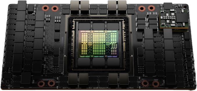
Depending on your point of view, the last two years have either gone by very slowly, or very quickly. While the COVID pandemic never seemed to end – and technically still hasn’t – the last two years have whizzed by for the tech industry, and especially for NVIIDA. The company launched its Ampere GPU architecture just two years ago at GTC 2020, and after selling more of their chips than ever before, now in 2022 it’s already time to introduce the next architecture. So without further ado, let’s talk about the Hopper architecture, which will underpin the next generation of NVIDIA server GPUs.
As has become a ritual now for NVIDIA, the company is using its Spring GTC event to launch its next generation GPU architecture. Introduced just two years ago, Ampere has been NVIDIA’s most successful server GPU architecture to date, with over $10B in data center sales in just the last year. And yet NVIDIA has little time to rest on their laurels, as the the growth and profitability of the server accelerator market means that there are more competitors than ever before aiming take a piece of NVIDIA’s market for themselves. To that end, NVIDIA is ready (and eager) to use their biggest show of the year to talk about their next generation architecture, as well as the first products that will implement it.
Taking NVIDIA into the next generation of server GPUs is the Hopper architecture. Named after computer science pioneer Grace Hopper, the Hopper architecture is a very significant, but also very NVIDIA update to the company’s ongoing family of GPU architectures. With the company’s efforts now solidly bifurcated into server and consumer GPU configurations, Hopper is NVIDIA doubling down on everything the company does well, and then building it even bigger than ever before.
Hyperbole aside, over the last several years NVIDIA has developed a very solid playbook for how to tackle the server GPU industry. On the hardware side of matters that essentially boils down to correctly identifying current and future trends as well as customer needs in high performance accelerators, investing in the hardware needed to handle those workloads at great speeds, and then optimizing the heck out of all of it. And for NVIDIA, the last step may very well be the most important bit: NVIDIA puts a lot of work into getting out of doing work.
That mentality, in turn, is front and center for NVIDIA’s Hopper architecture. While NVIDIA has made investments across the board to improve performance, from memory bandwidth and I/O to machine learning and confidential computing, the biggest performance uplifts with Hopper are in the areas where NVIDIA has figured out how to do less work, making their processors all the faster.
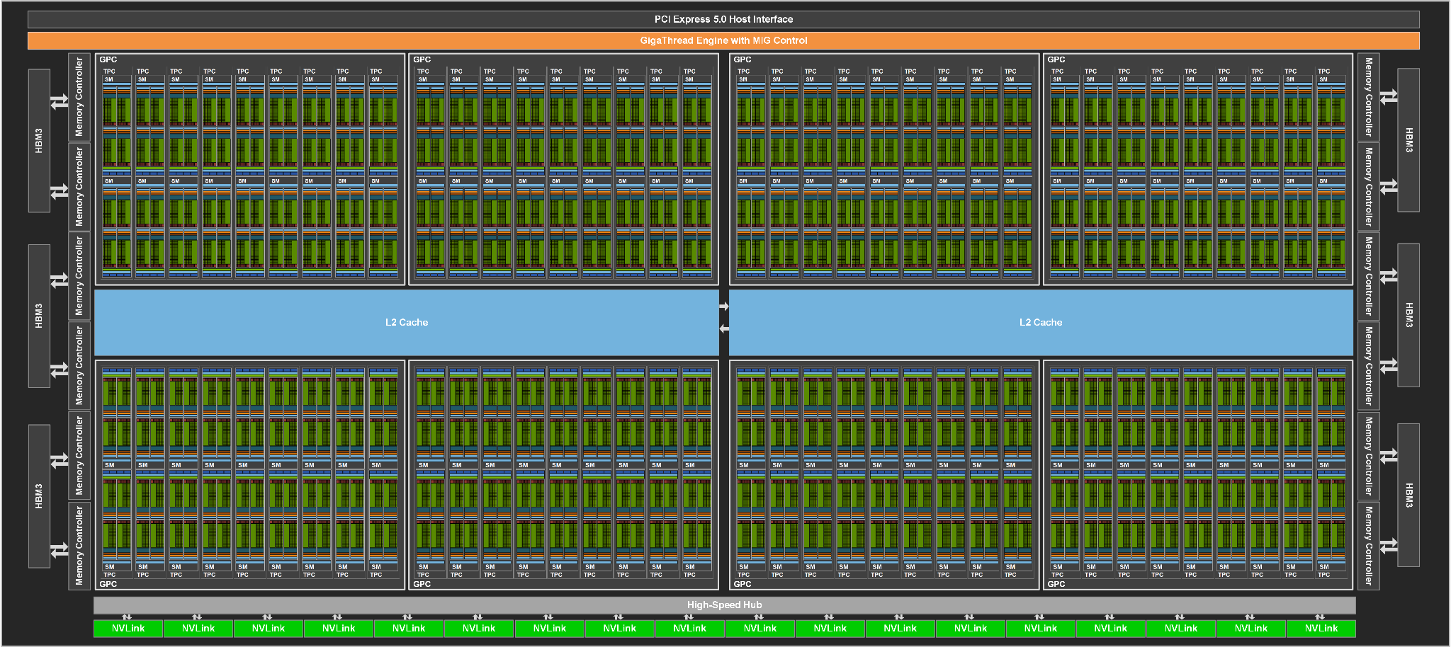
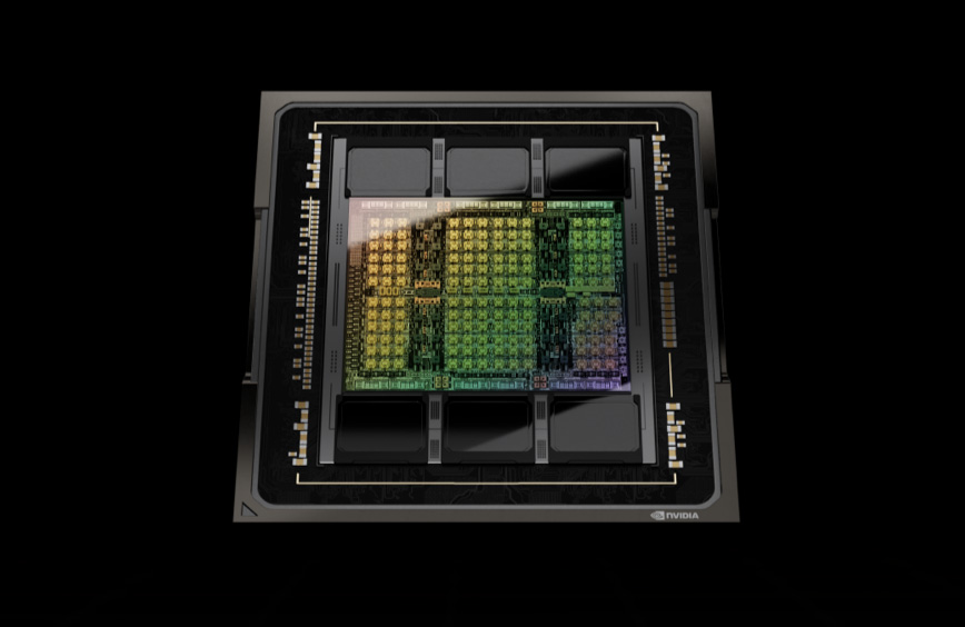
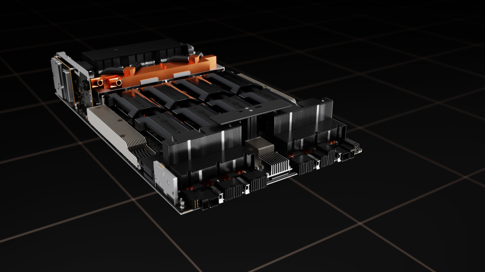
Kicking things off for the Hopper generation is H100, NVIDIA’s flagship server accelerator. Based on the GH100 GPU, GH100 is a traditional NVIDIA server-first launch, with the company starting at the high end to develop accelerator cards for their largest and deepest pocketed server and enterprise customers.
| NVIDIA Accelerator Specification Comparison | |||||
| H100 | A100 (80GB) | V100 | |||
| FP32 CUDA Cores | 16896 | 6912 | 5120 | ||
| Tensor Cores | 528 | 432 | 640 | ||
| Boost Clock | ~1.78GHz (Not Finalized) |
1.41GHz | 1.53GHz | ||
| Memory Clock | 4.8Gbps HBM3 | 3.2Gbps HBM2e | 1.75Gbps HBM2 | ||
| Memory Bus Width | 5120-bit | 5120-bit | 4096-bit | ||
| Memory Bandwidth | 3TB/sec | 2TB/sec | 900GB/sec | ||
| VRAM | 80GB | 80GB | 16GB/32GB | ||
| FP32 Vector | 60 TFLOPS | 19.5 TFLOPS | 15.7 TFLOPS | ||
| FP64 Vector | 30 TFLOPS | 9.7 TFLOPS (1/2 FP32 rate) |
7.8 TFLOPS (1/2 FP32 rate) |
||
| INT8 Tensor | 2000 TOPS | 624 TOPS | N/A | ||
| FP16 Tensor | 1000 TFLOPS | 312 TFLOPS | 125 TFLOPS | ||
| TF32 Tensor | 500 TFLOPS | 156 TFLOPS | N/A | ||
| FP64 Tensor | 60 TFLOPS | 19.5 TFLOPS | N/A | ||
| Interconnect | NVLink 4 18 Links (900GB/sec) |
NVLink 3 12 Links (600GB/sec) |
NVLink 2 6 Links (300GB/sec) |
||
| GPU | GH100 (814mm2) |
GA100 (826mm2) |
GV100 (815mm2) |
||
| Transistor Count | 80B | 54.2B | 21.1B | ||
| TDP | 700W | 400W | 300W/350W | ||
| Manufacturing Process | TSMC 4N | TSMC 7N | TSMC 12nm FFN | ||
| Interface | SXM5 | SXM4 | SXM2/SXM3 | ||
| Architecture | Hopper | Ampere | Volta | ||
Ahead of today’s keynote presentation – which as this article goes up, is still going on – NVIDIA offered a press pre-briefing on Hopper. In traditional NVIDIA fashion, the company has been very selective about the details released thus far (least it gets leaked ahead of Jensen Huang’s keynote). So we can’t make a fully apples-to-apples comparison to A100 quite yet, as we don’t have the full specifications. But based on this pre-briefing, we can certainly tease out some interesting highlights about NVIDIA’s architecture.
First and foremost, NVIDIA is once again building big for their flagship GPU. The GH100 GPU is comprised of 80 billion transistors and is being built on what NVIDIA is calling a “custom” version of TSMC’s 4N process node, an updated version of TSMC’s N5 technology that offers better power/performance characteristics and a very modest improvement in density. So even at just two years after Ampere, NVIDIA is making a full node jump and then some for GH100. At this point NVIDIA is not disclosing die sizes, so we don’t have exact figures to share. But given the known density improvements of TSMC’s process nodes, GH100 should be close in size to the 826mm2 GA100. And indeed, it is, at 814mm2.
Like NVIDIA’s previous sever accelerators, the H100 card isn’t shipping with a fully-enabled GPU. So the figures NVIDIA is providing are based on H100 as implemented, with however many functional units (and memory stacks) are enabled.
In regards to performance, NVIDIA isn’t quoting any figures for standard vector performance in advance. They are however quoting tensor performance, which depending on the format is either 3x or 6x faster than the A100 accelerator. We’ll see how this breaks down between clockspeed increases and either larger or additional tensor cores, but clearly NVIDIA is once again throwing even more hardware at tensor performance, a strategy that has worked out well for them so far.
Officially, NVIDIA likes to quote figures with sparsity enabled, but for the purposes of our spec sheet I’m using the non-sparse numbers for a more apples-to-apples comparison with previous NVIDIA hardware, as well as competing hardware. With sparsity enabled, TF32 performance and on down can be doubled.
Memory bandwidth is also improving significantly over the previous generation, with H100 offering 3TB/second of bandwidth there. The increase in bandwidth this time around comes thanks to the use of HBM3, with NVIDIA becoming the first accelerator vendor to use the latest-generation version of the high bandwidth memory. H100 will come with 6 16GB stacks of the memory, with 1 stack disabled. The net result is 80GB of HBM3 running at a data rate of 4.8Gbps/pin, and attached to a 5120-bit memory bus.
NVIDIA will be offering H100 in their usual two form factors: SXM mezzanine for high performance servers, and a PCIe card for more mainstream servers. The power requirements for both form factors have gone up significantly over the previous generation. NVIDIA is quoting an eye-popping 700 Watt TDP for the SXM version of the card, 75% higher than the official 400W TDP of the A100. For better or worse, NVIDIA is holding nothing back here, though the ongoing decline in transistor power scaling is not doing NVIDIA any favors, either.
Cooling such a hot GPU will be an interesting task, though not beyond current technology. At these power levels we’re almost certainly looking at liquid cooling, something the SXM form factor is well-suited for. Still, it’s worth noting that the rival OAM form factor – essentially the Open Compute Project’s take on SXM for use in accelerators – is designed to top out at 700W. So NVIDIA is seemingly approaching the upper limits of what even a mezzanine style card can handle, assuming that sever vendors don’t resort to exotic cooling methods.
Meanwhile the H100 PCie card will see its TDP raised to 350W, from 300W today. Given that 300W is the traditional limit for PCIe cards, it will be interesting to see how NVIDIA and their partners keep those cards cool. Otherwise, with just half the TDP of the SXM card, we’re expecting the PCIe version to be clocked/configured noticeably slower in order to temper the card’s power consumption.
Hopper Tensor Cores: Now With Transformer Engines
Moving on to the big-ticket architectural features of the Hopper architecture, we’re start with NVIDIA’s Transformer Engines. Living up to their name, the transformer engines are a new, highly specialized type of tensor core, that are designed to further accelerate transformer ML models.
In keeping with NVIDIA’s focus on machine learning, for the Hopper architecture the company has taken a fresh look at the makeup of the ML market, and what workloads are popular and/or the most demanding on existing hardware. The winner, in this regard, has been transformers, a type of deep learning model that have risen in popularity rather quickly due to their utility in natural language processing and computer vision. Recent advancements in transformer technology, such as the GPT-3 model, along with demand from service operators for better natural language processing, have made transformers the latest big breakthrough in ML.
But at the same time, the processing requirements for transformers are also hampering the development of even better models. In short, better models require an ever-larger number of parameters, and at over 175 billion parameters for GPT-3 alone, training times for transformers are becoming unwieldy, even on large GPU clusters.
To that end, NVIDIA has developed a variant of the tensor core specifically for speeding up transformer training and inference, which they have dubbed the Transformer Engine. NVIDIA has optimized this new unit by stripping it down to just processing the lower precision data formats used by most transformers (FP16), and then scaling things down even more with the introduction of an FP8 format as well. The goal with the new units, in brief, is to use the minimum precision necessary at every step to train transformers without losing accuracy. In other words, to avoid doing more work than is necessary.
![]()
With that said, unlike more traditional neural network models which are trained at a fixed precision throughout, NVIDIA’s latest hack for transformers is to vary the precision, since FP8 cannot be used throughout a model. As a result, Hopper’s transformer engines can swap between FP16 and FP8 training on a layer by layer basis, utilizing NVIDIA-provided heuristics that work to select the lowest precision needed. The net benefit is that every layer that can be processed at FP8 can be processed twice as fast, as the transformer engines can pack and process FP8 data twice as quickly as FP16.
Combined with the additional memory on H100 and the faster NVLink 4 I/O, and NVIDIA claims that a large cluster of GPUs can train a transformer up to 9x faster, which would bring down training times on today’s largest models down to a more reasonable period of time, and make even larger models more practical to tackle.
Meanwhile, on the inference side of matters, Hopper can also immediately consume its own FP8 trained models for inference use. This is an important distinction for Hopper, as it allows customers to otherwise skip converting and optimizing a trained transformer model down to INT8. NVIDIA isn’t claiming any specific performance benefits from sticking with FP8 over INT8, but it means developers can enjoy the same performance and memory usage benefits of running inference on an INT8 model without the previously-required conversion step.
Finally, NVIDIA is claiming anywhere between a 16x and 30x increase in transformer inference performance on H100 versus A100. Like their training claims, this is an H100 cluster versus an A100 cluster, so memory and I/O improvements are also playing a part here, but it none the less underscores that H100’s transformer engines aren’t just for speeding up training.
DPX Instructions: Dynamic Programming for GPUs
NVIDIA’s other big smart-and-lazy improvement for the Hopper architecture comes courtesy of the field of dynamic programming. For their latest generation of technology, NVIDIA is adding support for the programming model by adding a new set of instructions just for dynamic programming. The company is calling these DPX Instructions.
Dynamic programming, in a nutshell, is a way of breaking down complex problems into smaller, simpler problems in a recursive manner, and then solving those smaller problems first. The key feature of dynamic programming is that if some of these sub-problems are identical, then those redundancies can be identified and eliminated – meaning a sub-problem can be solved once, and its results saved for future use within the larger problem.
All of which is to say that, like Sparsity and Transformer Engines, NVIDIA is implementing dynamic programming to allow their GPUs to get out of doing more work. By eliminating the redundant parts of workloads that can be broken up per the rules of dynamic programming, it’s that much less work NVIDIA’s GPUs need to do, and that much faster they can produce results.
Though unlike Transformer Engines, adding dynamic programming support via the DPX Instructions is not so much about speeding up existing workloads on GPUs as it is enabling new workloads on GPUs. Hopper is the first NVIDIA architecture to support dynamic programming, so workloads that can be resolved with dynamic programming are normally run on CPUs and FPGAs. In that respect, this is NVIDIA finding one more workload they can steal from CPUs and run on a GPU instead.
Overall, NVIDIA is claiming a 7x improvement in dynamic programming algorithm performance on a single H100 versus naïve execution on an A100.
As for the real-world implications of DPX Instructions, NVIDIA is citing route planning, data science, robotics, and biology as all being potential beneficiaries of the new technology. These fields already use several well-known dynamic programming algorithms, such as Smith-Waterman and Flyod-Warshall, which score genetic sequence aligning and find the shortest distances between pairs of destinations respectively.
Overall, dynamic programming is one of the more niche fields among high performance workloads. But it’s one that NVIDIA believes can be a good fit for GPUs once the right hardware support is available.
Confidential Computing: Protecting GPU Data From Prying Eyes
Shifting away from performance-focused features, NVIDIA’s other big push with the Hopper architecture is on the security front. With the expansion of GPU usage in cloud computing environments – and especially shared VM environments – the company is taking a new focus on the security concerns that entails, and how to secure shared systems.
The end result of those efforts is that Hopper is introducing hardware support for trusted execution environments. Specifically, Hopper supports the creation of what NVIDIA is terming a confidential virtual machine, where all of the data within the VM environment is secure, and all of the data entering (and leaving) the environment is encrypted.
NVIDIA didn’t go over too many of the technical details underpinning their new security features in our-pre-briefing, but according to the company it’s a product of a mix of new hardware and software features. Of particular note, data encryption/decryption when moving to and from the GPU is fast enough to be done at the PCIe line rate (64GB/sec), meaning there’s no slowdown in terms of practical host-to-GPU bandwidth when using this security feature.
This trusted execution environment, in turn, is designed to resist all forms of tampering. The memory contents within the GPU itself are secured by what NVIDIA is terming a “hardware firewall”, which prevents outside processes from touching them, and this same protection is extended to data in-flight in the SMs as well. The trusted environment is also said to be secured against the OS or the hypervisor accessing the contents of the GPU from above, restricting access to just the owner of the VM. Which is to say that, even with physical access to the GPU, it shouldn’t be possible to access the data within a secure VM on hopper.
Ultimately, NVIDIA’s aim here appears to be making/keeping their customers comfortable using GPUs to process sensitive data by making them much hardware to break into when they’re working in a secured mode. This, in turn, is not only to protect traditionally sensitive data, such as medical data, but also to protect the kind of high-value AI models that some of NVIDIA’s customers are now creating. Given all of the work that can go into creating and training a model, customers don’t want their models getting copied, be it in a shared cloud environment or being pulled out of a physically insecure edge device.
Multi-Instance GPU v2: Now With Isolation
As an extension of NVIDIA’s security efforts with confidential computing, the company has also extended these protections to their Multi-Instance GPU (MIG) environment. MIG instances can now be fully isolated, with I/O between the instance and the host fully virtualized and secured as well, essentially granting MIG instances the same security features as H100 overall. Overall, this moves MIG closer to CPU virtualization environments, where the various VMs assume not to trust each other and are kept isolated.
NVLink 4: Extending Chip I/O Bandwidth to 900GB/sec
With the Hopper architecture also comes a new rendition of NVIDIA’s NVLink high-bandwidth interconnect for wiring up GPUs (and soon, CPUs) together for better performance in workloads that can scale out over multiple GPUs. NVIDIA has iterated on NVLink with every generation of their flagship GPU, and this time is no different, with the introduction of NVLink 4.
While we’re awaiting a full disclosure of technical specifications from NVIDIA, the company has confirmed that NVLink bandwidth on a per-chip basis has been increased from 600GB/second on A100 to 900GB/second for H100. Note that this is the sum total of all upstream and downstream bandwidth across all of the individual links that NVLink supports, so cut these figures in half to get specific transmit/receive rates.
| NVLink Specification Comparison | |||||
| NVLink 4 | NVLink 3 | NVLink 2 | |||
| Signaling Rate | 100 Gbps | 50 Gbps | 25 Gbps | ||
| Lanes/Link | 2 | 4 | 8 | ||
| Bandwidth/Direction/Link | 25 GB/sec | 25 GB/sec | 25 GB/sec | ||
| Total Bandwidth/Link | 50 GB/sec | 50 GB/sec | 50 GB/sec | ||
| Links/Chip | 18 (GH100) |
12 (GA100) |
6 (GV100) |
||
| Bandwidth/Chip | 900 GB/sec | 600 GB/sec | 300 GB/sec | ||
900GB/sec represents a 50% increase in I/O bandwidth for H100. Which is not as great an increase as H100’s total processing throughput, but a realistic improvement given the ever-escalating complexities in implementing faster networking rates.
Given that NVLink 3 was already running at a 50 Gbit/sec signaling rate, it’s not clear if the additional bandwidth is courtesy of an even faster signaling rate, or if NVIDIA has once again adjusted the number of links coming from the GPU. NVIDIA previously altered the NVLink lane configuration for A100, when they halved the lane width and doubled the number of lanes, all while doubling the signaling rate. Adding lanes on top of that means not having to figure out how to improve the signaling rate by even more, but it also means a 50% increase in the number of pins needed for NVLink I/O.
Along those lines, it’s also worth noting that NVIDIA is adding PCIe 5.0 support with Hopper. As PCIe is still used for host-to-GPU communications (until Grace is ready, at least), this means NVIDIA has doubled their CPU-GPU bandwidth, letting them keep H100 that much better fed. Though putting PCIe 5.0 to good use is going to require a host CPU with PCIe 5.0 support, which isn’t something AMD or Intel are providing quite yet. Presumably, someone will have hardware ready and shipping by the time NVIDIA ships H100 in Q3, especially since NVIDIA is fond of homogenization for their DGX pre-built servers.
Finally, with the launch of H100/NVLink 4, NVIDIA is also using this time to announce a new, external NVLink switch. This external switch extends beyond NVIDIA’s current on-board NVSwitch functionality, which is used to help build more complex GPU topologies within a single node, and allows H100 GPUs to directly communicate with each other across multiple nodes. In essence, it’s a replacement for having NVIDIA GPUs go through Infiniband networks in order to communicate cross-node.
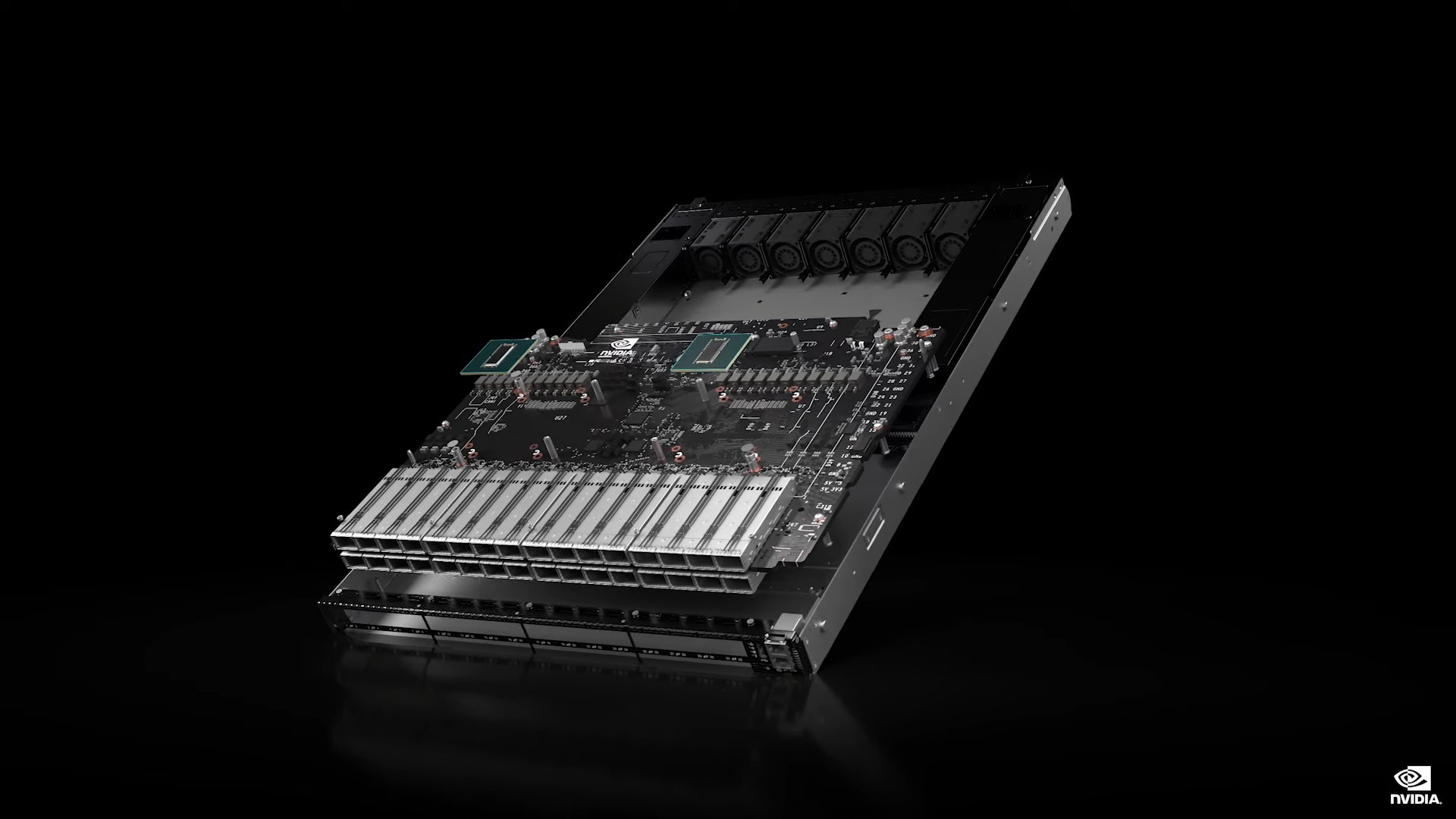
The external NVLInk Switch allows for up to 256 GPUs to be connected together within a single domain, which works out to 32 8-way GPU nodes. According to NVIDIA, a single, 1U NVLink Switch offers 128 lanes of NVLink via 32 Octal SFP (OSFP) transceivers. The full Switch, in turn, offers a total bisection bandwidth of 70.4TB/second.
It’s worth noting, however, that the NVLink Switch is not a wholesale replacement for Infiniband – which of course, NVIDIA also sells through its networking hardware division. Infiniband connections between nodes are still needed for other types of communications (e.g. CPU to CPU), so external NVLink networks are a supplement to Infiniband, allowing H100 GPUs to directly chat amongst themselves.
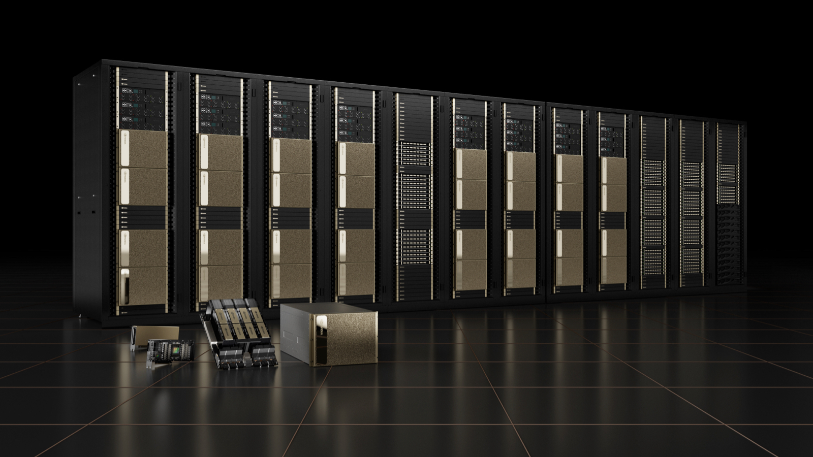
NVIDIA HGX Rides Again: HGX For H100
Last, but not least, NVIDIA has confirmed that they’re updating their HGX baseboard ecosystem for H100 as well. A staple of NVIDIA’s multi-GPU designs since they first began using the SXM form factor for GPUs, HGX baseboards are NVIDIA-produced GPU baseboards for system builders to use in designing complete multi-GPU systems. The HGX boards provide the full connection and mounting environment for NVIDIA’s SXM form factor GPUs, and then sever vendors can route power and PCIe data (among other things) from their motherboards to the HGX baseboard. For the current A100 generation, NVIDIA has been selling 4-way, 8-way, and 16-way designs.
Relative to the GPUs themselves, HGX is rather unexciting. But it’s an important part of NVIDIA’s ecosystem. Server partners can pickup an HGX board and GPUs, and then quickly integrate that into a server design, rather than having to design their own server from scratch. Which in the case of H100, means that status quo will (largely) reign, and that NVIDIA’s server partners will be able to assemble systems in the same manner as before.
Hopper H100 Accelerators: Shipping In Q3 2022
Wrapping things up, NVIDIA is planning on having H100-equipped systems available in Q3 of this year. This will include NVIDIA’s full suite of self-built systems, including DGX and DGX SuperPod servers, as well as servers from OEM partners using HGX baseboards and PCIe cards. Though in typical fashion, NVIDIA is not announcing individual H100 pricing, citing the fact that they sell this hardware through server partners. We’ll have a bit more insight once NVIDIA announces the prices of their own DGX systems, but suffice it to say, don’t expect H100 cards to come cheap.


88 Comments
View All Comments
mode_13h - Thursday, March 24, 2022 - link
The other point I was going to make is that I wonder how much on-die memory they have. This seems to be the growing trend in deep learning & data-flow processors. GPUs are good at hiding latency, but it's even better not to have high latency, in the first place.Also, data movement + lookups in cache tag RAM are probably where Nvidia is burning a significant chunk of power.
CiccioB - Thursday, March 24, 2022 - link
<blockquote>Also, data movement + lookups in cache tag RAM are probably where Nvidia is burning a significant chunk of power.</blockquote>Until there will be the tech to put several GB of SRAM directly and cheaply on GPU die that kind of inefficiency has to be taken into account.
All you can do meanwhile is trying to re-use data and results as much as possible without moving them back and forth, and it seems Nvidia has been targeting this goal with some of the new features added to Hopper.
mode_13h - Friday, March 25, 2022 - link
> Until there will be the tech to put several GB of SRAM directly and> cheaply on GPU die that kind of inefficiency has to be taken into account.
That's a false dichotomy. Nvidia can increase their SRAM substantially, without going all the way to GBs. And I was merely wondering how much they have, because it's an undeniable trend.
FWIW, each SM in the A100 has "unified data cache and shared memory with a total size of 192 KB", with up to 164 KB of it being configurable as shared memory. So, that's about 20.25 MB of on-die SRAM of which up to 17.3 MB is directly-addressable. Relative to the amount of compute power it has, I think that's smaller than what competing AI silicon tends to feature.
So far, the figures I've managed to find are 900 MB for a 1472-core Graph Core chip, Xilinx Versal AI Edge claiming 38 MB for a "mid-range" implementation, 300 MB for SambaNova's Cardinal SN10 RDU, 160 MB for Esperanto's 1k core RISC-V chip, Qualcomm AI100 has 144 MB, and Cerebras WSE-2 featuring 40 GB. Obviously, that Cerbras is not a fair comparison.
Also, worth noting: DE Shaw's ANTON 3 features 66 MB of SRAM, but that's a purpose-built chip for molecular dynamics simulations.
mode_13h - Friday, March 25, 2022 - link
Forgot to add that most/all of those are TSMC N7. I got a lot of them from the Hot Chips 2021 presentations. I didn't bother to look through the 2020 set.CiccioB - Friday, March 25, 2022 - link
The amount of data you can keep on-die helps greatly to decrease both access latency and also transfer power.That's a fact, not a "false dichotomy", as there is no dichotomy here.
GH100 is a 800mm^2 and beyond chip filled with any possible calculation unit to be able to execute any sort of work thrown at it. The amount of cache that it can hold inside the die is small, or you would have to sacrifice brute force or some unit entirely diminishing its flexibility.
It has 60MB of cache as whole, but would it also be 120MB or 320MB, it may be too few nonetheless.
This monster can elaborate 3TB/s of data in a second, you can see yourself those cache are ridiculously small to not pretend that a lot of data still comes and go to the HBM stack also as a temporary place to be accessed again later.
Probably putting something as a 3D cache on it, reaching several hundreds of fast SRAM would help a lot in lowering data movement outside the die.
However, cache and SRAM suck energy by themselves so you have to compromise the energy for keeping data near the cores and that used for transfer useless data far away to the HBM stack.
I suppose Nvidia did its calculations, both in terms of performance, cost, thermal and probabilities and did what they could to try to lease the data transfer power consumption issue with the transistor budget they had. That does not mean that having bigger caches (or a L3 cache on separate 3D die) would not help in such a data swallower monster.
CiccioB - Friday, March 25, 2022 - link
You may see what Nvidia has done for this data transfer problem directly from the description of their own architecture:* New thread block cluster feature enables programmatic control of locality at a granularity larger than a single thread block on a single SM. This extends the CUDA programming model by adding another level to the programming hierarchy to now include threads, thread blocks, thread block clusters, and grids. Clusters enable multiple thread blocks running concurrently across multiple SMs to synchronize and collaboratively fetch and exchange data.
* Distributed shared memory allows direct SM-to-SM communications for loads, stores, and atomics across multiple SM shared memory blocks.
* New asynchronous execution features include a new Tensor Memory Accelerator (TMA) unit that can transfer large blocks of data efficiently between global memory and shared memory. TMA also supports asynchronous copies between thread blocks in a cluster. There is also a new asynchronous transaction barrier for doing atomic data movement and synchronization.
* 50 MB L2 cache architecture caches large portions of models and datasets for repeated access, reducing trips to HBM3.
On complete chip L2 cache amount to 60 MB.
mode_13h - Saturday, March 26, 2022 - link
> You may see what Nvidia has done for this data transfer problemThese help them get more use out of what they have, but are ultimately limited in how much they can compensate for lack of quantity.
> Tensor Memory Accelerator
Doesn't appear to reduce data movement, thus energy utilization. All it does is hep the compute units stay busy doing actual computation. That's only tackling half the problem.
Mike Bruzzone - Monday, March 28, 2022 - link
And X and F variants are where on their L3 low latency aims? I wonder what compliment that hooks up too? mbmode_13h - Saturday, March 26, 2022 - link
> That's a fact, not a "false dichotomy", as there is no dichotomy here.You quoted me saying:
me> data movement + lookups in cache tag RAM are probably where Nvidia
me> is burning a significant chunk of power." and then claimed:
you> Until there will be the tech to put several GB of SRAM directly and cheaply
you> on GPU die that kind of inefficiency has to be taken into account.
The false dichotomy is that there's no use trying to mitigate the cost of cache & data movement until you can put GB of RAM on die.
I quoted numerous examples where (mostly) AI processors competing with Nvidia reached a different conclusion. Some went as far as to say they didn't even need HBM, due to the amount of on-die SRAM they had, instead using conventional DDR4 for bulk storage.
If you know anything about the data-access patterns involved in neural net inferencing, this makes perfect sense. The weights tend to be much larger than the data propagating through the network. So, the more on-die storage you have, the less you need to page them in from DRAM, assuming you can do some form of batch-processing.
> GH100 is a 800mm^2 and beyond chip filled with any possible calculation unit
> to be able to execute any sort of work thrown at it. The amount of cache that
> it can hold inside the die is small, or you would have to sacrifice brute force or
> some unit entirely diminishing its flexibility.
This is a silly argument. All of these chips are optimized to do heavy computation. Your only legit point is that maybe some of the H100's target workloads, besides AI, lack the same degree of locality. So, maybe they chose to hurt AI performance a little bit, in order to devote more die area to things like fp64, so they could better counter AMD on that front.
> It has 60MB of cache as whole
Well, it's not ideal to have as cache, for the reasons I mentioned. The software is already custom-tuned for the GPU, so you might as well use directly-addressable SRAM and avoid the energy & latency penalty of the tag lookups.
Now that I'm looking at Nvidia's blog, I see they have up to 26 MB of on-die "shared memory". The "up to" part is a reference that some amount of it could be used as either cache or directly-addressable, which makes it clear they understand the benefits. Otherwise, they'd just make it all cache.
> This monster can elaborate 3TB/s of data in a second
That burns a lot of power. It's better if you can optimize your memory hierarchy and data access patterns to keep the most frequent accesses on-die. Some of those Hot Chips presentations I poured through to collect the SRAM tallies in my prior post mentioned far greater throughput, like I think one mentioned 12 TB/sec and GraphCore mentioned 62 TB/sec for accessing their SRAM contents.
> those cache are ridiculously small to not pretend that a lot of data still comes
> and go to the HBM stack also as a temporary place to be accessed again later.
900 MB is ridiculously small? Also, you don't seem to know anything about the data access patterns in question. When building high-performance hardware, it pays to know something about the software it's intended to run. Ideally, the hardware and software should be co-optimized.
> Probably putting something as a 3D cache on it, reaching several hundreds
> of fast SRAM would help a lot in lowering data movement outside the die.
One of those I mentioned used 3D stacking, but I think GraphCore (the one with 896 MB) didn't. They say half the die is SRAM.
> I suppose Nvidia did its calculations, both in terms of performance, cost, thermal
GraphCore claims their entire quad-processor chassis uses 800-1200 W typical, 1500W peak
> transistor budget
GraphCore's is 59.6 B, which they say is TSMC's biggest N7 chip.
I definitely think Nvidia generally knows what they're doing. That's why I expected more on-die SRAM. However, it's risky to assume that just because Nvidia did something one way, that it's optimal. Nvidia is tackling a broader problem set than most of their competitors in the AI market. This could finally start to hurt them.
Mike Bruzzone - Monday, March 28, 2022 - link
mb