Intel Details PowerVia Chipmaking Tech: Backside Power Performing Well, On Schedule For 2024
by Ryan Smith on June 5, 2023 9:00 AM EST- Posted in
- CPUs
- Intel
- EUV
- IFS
- Intel 20A
- Intel 18A
- PowerVIA
- Arrow Lake
- Backside Power
- Crestmont
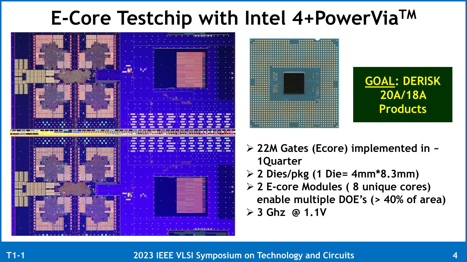
Blue Sky Creek: An Intel 4 + PowerVia Test Chip, Based on Crestmont E-Cores
To put PowerVia to the test and to prove that it’s working as expected, Intel’s validation vehicle for the technology is a chip they’re calling Blue Sky Creek.
Derived from Intel’s Meteor Lake platform, Blue Sky Creek uses two dies of E-cores that are based on Intel’s Crestmont CPU architecture. The reason Intel is using Crestmont here is two-fold: first, it was originally designed for Intel 4, making it a good candidate for porting over to the Intel 4 + PowerVia process. And second, because E-cores are tiny; the quad-core test dies are just 33.2mm2 (4mm x 8.3mm) in size, making them a good balance between complexity for testing and not having to actually yield a massive die on an experimental process node.
Intel isn’t focused too much on the performance of the E-cores in Blue Sky Creek. But they do note that the designed frequency was 3GHz at 1.1v.
With regards to the bigger picture, Big Sky Creek’s existence is part of Intel’s grand plan to mitigate the risk of introducing two major technological changes within the same process node – a problem that hit Intel rather hard with the overly-ambitious development plan for their 10nm (Intel 7) process node.
As outlined by the company back in 2022, of the two technologies, PowerVia was considered the riskier of the two. For that reason, Intel would be developing an interim test node just for PowerVia, allowing them to work on the technology separately from RibbonFETs. Ultimately, if PowerVia development had not progressed as expected, Intel could still do RibbonFET development, and bring out chips sans-PowerVia.
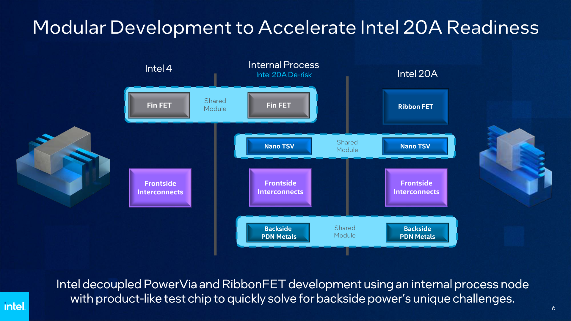
For similar reasons, you won’t find much discussion of RibbonFET from Intel for the VLSI conference. While it’s an important technology for the company, it’s essentially a sure-thing for Intel. The company won’t even be the first fab with GAAFET technology, so while RibbonFET does come with its own challenges, intel didn’t need to prepare any risk mitigation strategies for it in the same way as they did PowerVia.
PowerVia In Practice: Intel’s Finds 30% Reduction in IR Droop, 6% Higher Clockspeeds, Ready for HVM
Diving into the results of Intel’s PowerVia papers, the company has broken out their results for Blue Sky Creek on a metric-by-metric basis, looking at everything from chip density to performance to thermals.
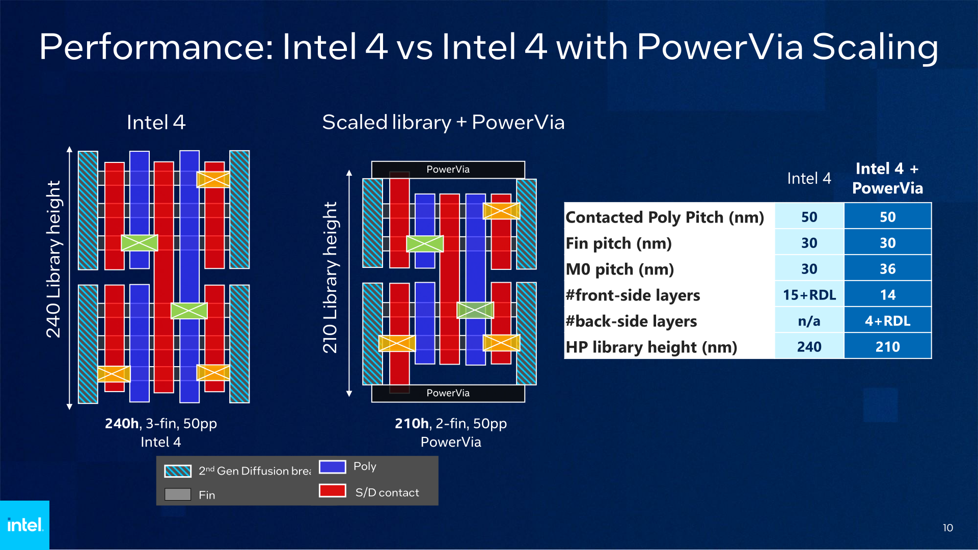
Starting with chip density, here’s a look at the size of the high performance (HP) library cells that Intel developed and fabbed for their test chip, and how those cells compare to the equivalent Intel 4 cells. As noted earlier, the shift to PowerVia has allowed Intel to relax the pitch of the critical M0 metal layer, enlarging it from 30 nm to 36 nm. The other major parameters of the node, such as the fin pitch and contacted poly pitch (CPP) remain at 30 nm and 50 nm respectively.
Yet, those changes, combined with Intel’s ability to reduce the number of fins in use from 3 to 2, result in an overall smaller cell. Thanks to PowerVia, Intel was able to bring the library height down to 210 nm, from 240 nm on Intel 4. And with the CPP holding constant at 50 nm, that means the overall cell size has been reduced by 12.5%, despite not using a formally “denser” node.
Meanwhile, this disclosure also gives us a proper look at the total number of layers involved in the two chips. Whereas a standard Intel 4 chip will have 15 layers plus the redistribution layer (RDL) all on one side, the PowerVia test chip had 14 layers on the signal (front) side, and another 4 layers plus the RDL on the power (back) side. That is a net gain of 3 layers overall, so at least as far as Intel’s test chip goes, it’s more complex in terms of the total number of layers used. But on the flip side, all of those new layers come on the power side of the chip, where they’re all relatively large and easy to fab. Which is why Intel considers the additional layers a minimal drawback compared to not having to manufacture a 30 nm pitch M0 layer.
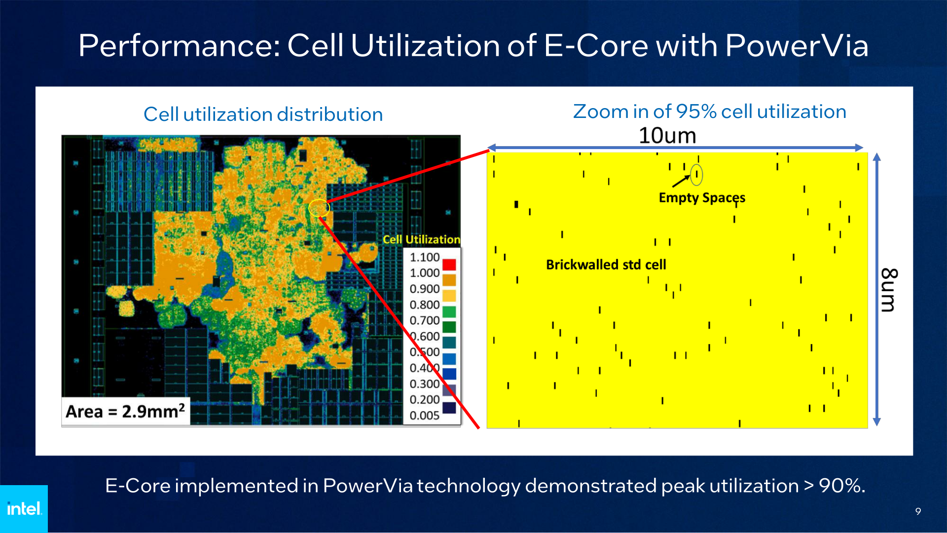
The density of these cells is also quite impressive. By moving to backside power delivery, Intel was able to utilize 95% of the space within one of the denser spots within the E-core cell. Unfortunately, Intel didn’t give comparable numbers for E-cores on Intel 4, but in general, the utilization is not quite that high.
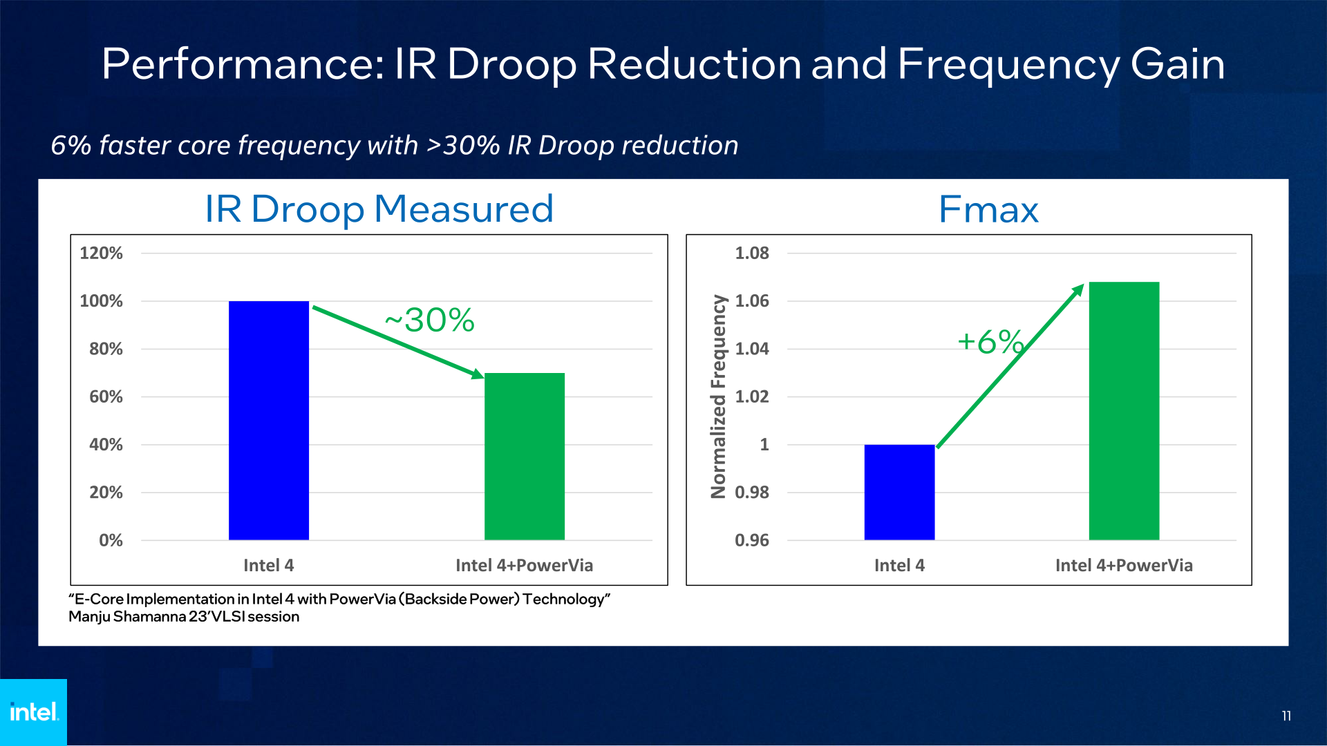
As for the electrical performance of the E-cores, as expected, PowerVia delivers a significant reduction in IR Doop. Intel measured a 30% reduction in droop on their test chip as compared to an Intel 4-built E-core, and an even greater 80% (5x) reduction in droop at the actual chip bump level.
That clean power delivery, in turn, improves the compute performance and the energy efficiency of the chip. Besides the direct efficiency gains from losing less energy to resistance, constructing an E-core with PowerVia technology improved the maximum frequency (fMax) of the core by 6%. Intel doesn’t offer a more detailed explanation as to why this improved their clockspeeds, but I suspect it has to do with a higher voltage actually reaching the transistors themselves, allowing them to clock a bit higher.
And while a 6% clockspeed uplift isn’t a massive gain, it’s essentially a “free” improvement coming from a technology that is designed to improve the manufacturability of a chip. Intel has worked harder to get smaller clockspeed improvements in the past.
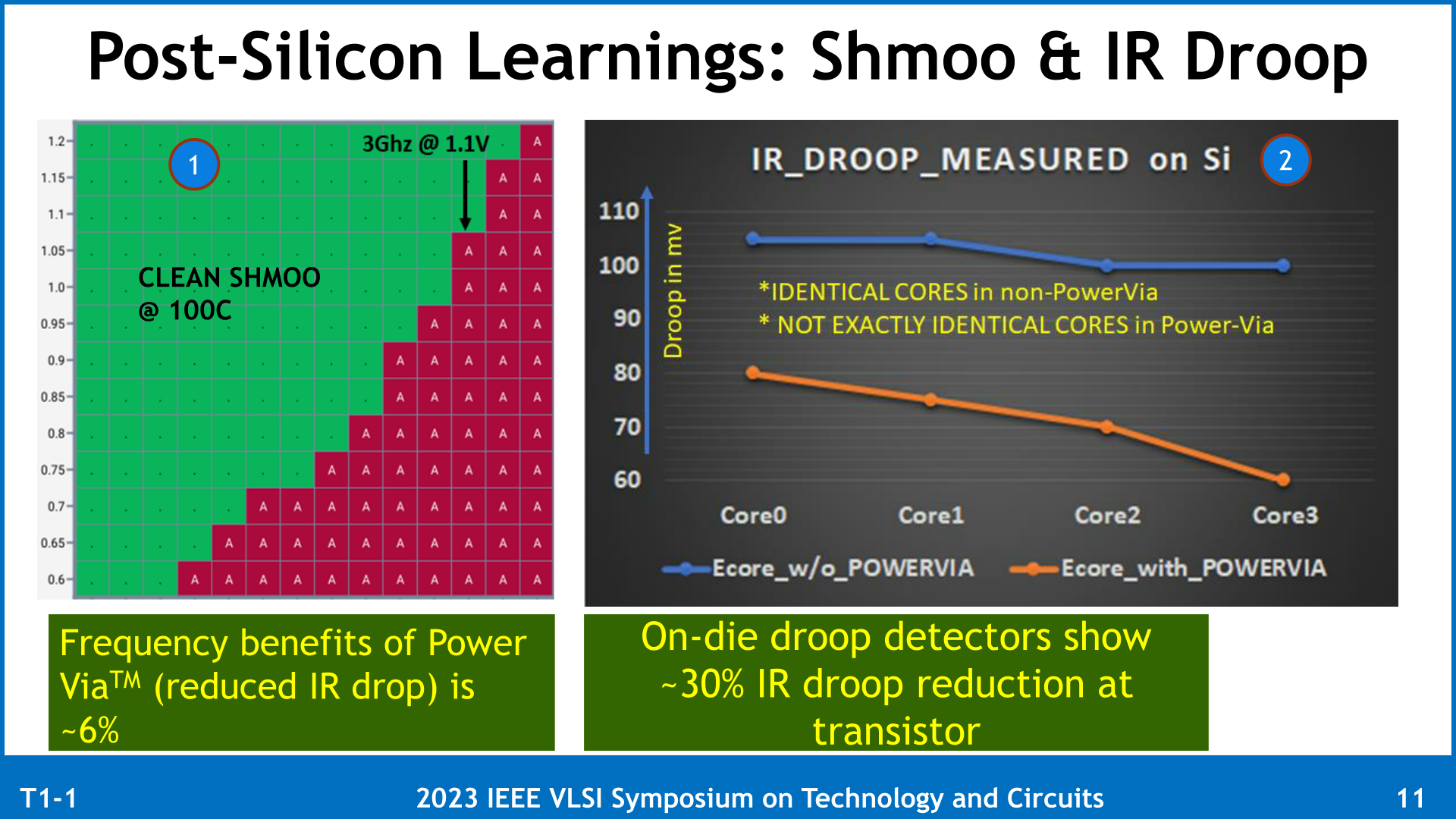
Interestingly, Intel did find that the new IR Droop values were not the same across all of the E-cores. Whereas the standard Intel 4 chip had a fairly consistent droop over all 4 cores, the droop for the test chip was between 60 mV and 80 mV, depending on the core. As this is a research presentation, Intel doesn’t go into the product ramifications of that, but assuming that production chips have a similarly wide range of variability, it may mean we see a greater emphasis on favored/prime cores in future products.
So PowerVia/BS-PDN works. But can Intel manufacture it at scale? The answer to that is also yes.
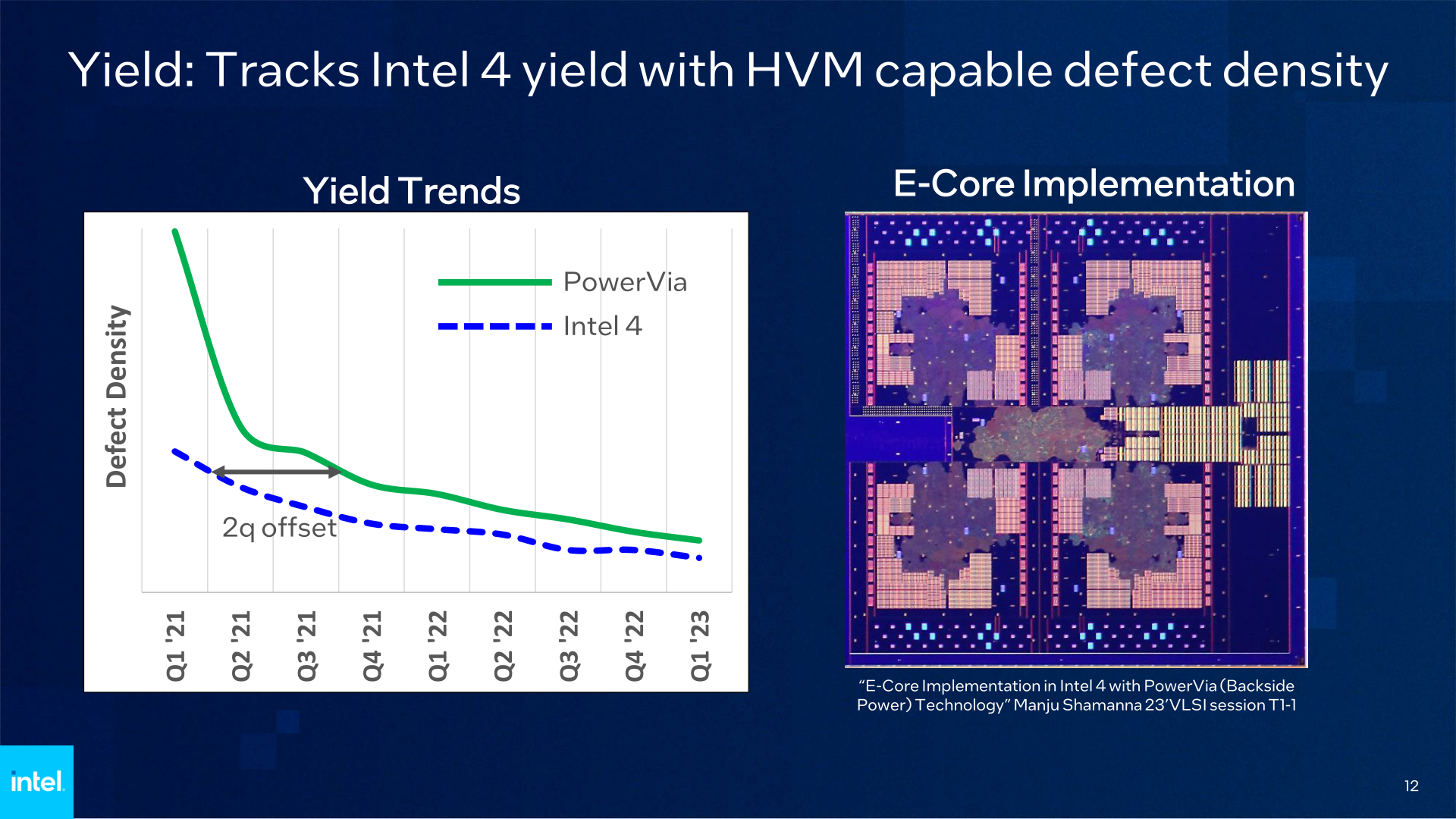
Accord to Intel, the defect density for their experimental Intel 4 + PowerVia process node is only about two quarters behind the Intel 4 process itself (which is already in HVM). Meaning that not only is the defect density low enough to be suitable for mass production in short order, but if Intel were scaling this specific node up for production, they would have similar chip yields as current, non-PowerVia Intel 4 chips in just two quarters.
Similarly, Intel reports that transistors built on the PowerVia process are very similar to those of the Intel 4 process. Which in this case, is very much a good thing, as it means those transistors aren’t doing unexpected things that impact performance or chip reliability. For that matter, Intel also noted that they observed no power-related reliability violations on the test chip, demonstrating that despite the significant changes to power delivery, the introduction of backside power delivery did not result in a less reliable power delivery system for the chip.
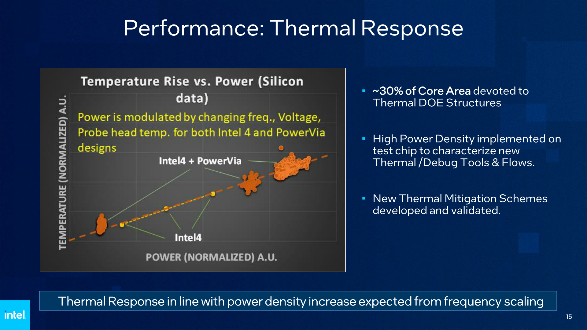
And while Intel isn’t going into the exact measures they’re employing to mitigate the thermal impacts of the transistor layer no longer being at the top of a flipped chip, the company is publishing data showing that the mitigations they have undertaken have been successful.
When plotted against the thermal response curve for an Intel 4 chip, Intel’s test chip demonstrated a very similar thermal response curve. Which is to say that at a given power level, the resulting temperatures were in-line with an Intel 4 chip. And as you may notice from Intel’s chart, they even went ahead and overfed the chip a bit to simulate even higher thermal loads, to better characterize the thermal response curve and to make sure thermal scaling wasn’t breaking down at higher thermal densities.
As noted earlier, thermals/cooling are one of the two big product-level challenges with backside power delivery. Placing transistors in what’s become the middle of the chip has not done chip cooling any favors, but Intel believes they have developed the necessary mitigation strategies to bring PowerVia chips in line with traditional frontside-fabbed flip chips.
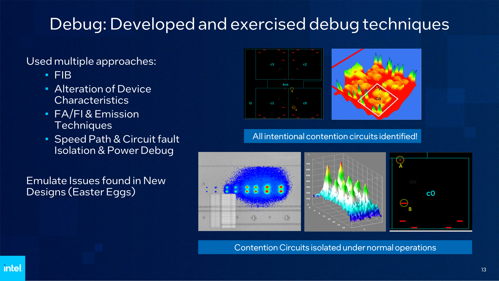
Those mitigations go for debugging, as well, which was the other challenge with BS-PDN. Intel has developed a suite of new and modified debugging techniques to deal with the fact that both sides of a chip are now in use. And while, to quote the abstract of Intel’s paper “Failure debug and defect isolation is complex due to the presence of metallization on both sides of the wafer,” ultimately, Intel was able to develop the necessary tools.
Interestingly, Intel even placed some “Easter Egg” defects within the chip’s design in order to provide some semi-controlled defects for Intel’s validation teams to work against. According to Intel their validation teams found all of those eggs with their PowerVia debugging tools, helping to prove the validity of those debug processes.
PowerVia To Land in Intel Chips in 2024
Wrapping things up, ahead of next week’s VLSI conference Intel is laying out a very convincing case that they are on the right track with their PowerVia backside power delivery technology development. Having a complex test chip up and running is a big deal in this regard, as having actual data and experience to draw from is a major step towards fine-tuning the technology for high volume manufacturing, all the while showcasing that Intel is so far meeting their aggressive fab development goals.
Ultimately, PowerVia is perhaps the single biggest make-or-break moment for Intel in terms of fully recovering momentum and potentially retaking leadership within the silicon lithography business. If Intel can deliver on its promises, the company is expecting to be at least two years ahead of TSMC and Samsung in deploying backside power delivery – and that means at least two years of reaping the cost and performance benefits of the technology. TSMC for its part is not expecting to deploy backside power until its N2P node in late 2026 or early 2027, while it remains unclear when Samsung will make their own transition.
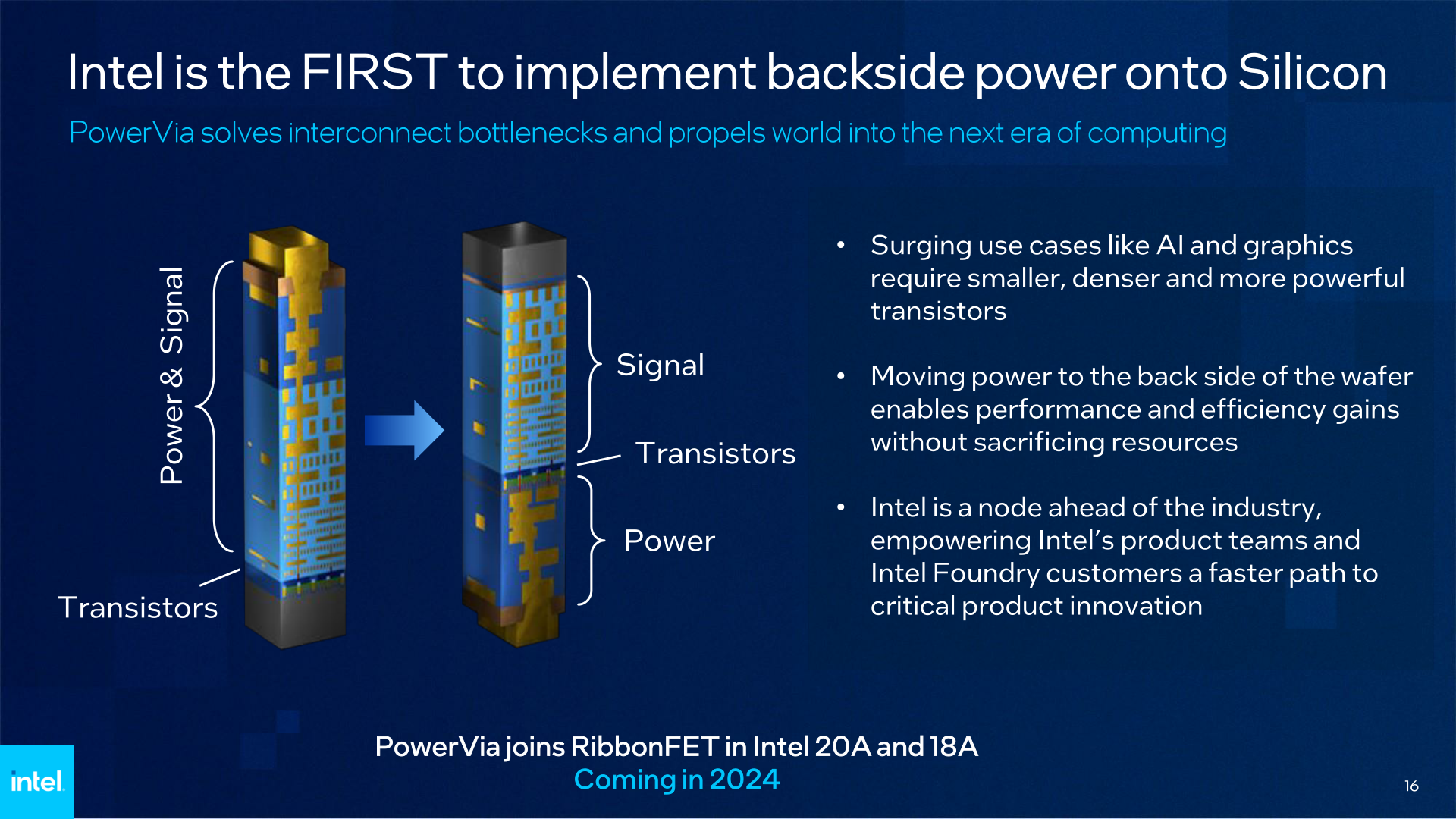


As for Intel, if everything continues to go to plan, Intel will begin high volume manufacturing with PowerVia in 2024, when the company is scheduled to bring both its Intel 20A and Intel 18A processes online. The first consumer processor to launch using the technology will be Intel’s Arrow Lake architecture, which will be a future generation Core product built on the 20A node.


31 Comments
View All Comments
dullard - Monday, June 5, 2023 - link
Intel 3 production will be ready to begin mass production ramping soon. Power Via isn't supposed to be ready until 2024. Intel burned themselves badly in the past by putting too many new things into one basket and couldn't deliver. I can see why they waited another generation.Ryan Smith - Monday, June 5, 2023 - link
The process node used here (Intel 4 + PowerVia) is only for R&D purposes. It is not a production node. PowerVia won't go into production until Intel 20A.Using Intel 3 as your base for the test node would have just made things take longer. Intel 3's advancements aren't pertinent to the development of BS-PDN.
(And if you're asking why Intel didn't make an Intel 3 + PowerVia production node, I point back to the fact that PowerVia won't be ready any earlier than in time for Intel 20A)
James5mith - Tuesday, June 6, 2023 - link
Not to skip too far ahead, but how will this impact GPU manufacturing?Modern GPUs are already pushing thermal boundaries with 400-700w power draw. Having to extract that heat through additional layers of silicon seems very very challenging for those higher power/heat situations.
my_wing - Tuesday, June 6, 2023 - link
Because PowerVIA is a more efficient way to power the transistor (6% mentioned), you pump less amps into the transistor and will create less heat.That clean power delivery, in turn, improves the compute performance and the energy efficiency of the chip. Besides the direct efficiency gains from losing less energy to resistance, constructing an E-core with PowerVia technology improved the maximum frequency (fMax) of the core by 6%. Intel doesn’t offer a more detailed explanation as to why this improved their clockspeeds, but I suspect it has to do with a higher voltage actually reaching the transistors themselves, allowing them to clock a bit higher. So you create 6% less heat in the first place, although we don't know how heat will leave the chip. We also don't know the structure of the dummy waffle, since before PowerVIA, the chip is package upside down and PowerVIA is the other way around, with the supportive dummy waffle on top. As heat goes up in physics, the structure/shape of the dummy waffle can be the difference to how heat is leaving the chip itself, are there holes in the dummy waffle, what is the shape of the holes, are those shape in anyway to help the heat leaving the chip, is the dummy waffle have a more heat conductive layer on top will that help the heat leaving the chip.
As Chip is moving from 2D to 2.5D/3D the mentioned joke about there are so little silicone left meaning that there are so many space(air) in between and where these spaces are will impact the heat leaving the chip.
From the article it read a follow:
And while a 6% clockspeed uplift isn’t a massive gain, it’s essentially a “free” improvement coming from a technology that is designed to improve the manufacturability of a chip. Intel has worked harder to get smaller clockspeed improvements in the past.
dwbogardus - Thursday, June 8, 2023 - link
Lower resistance isn't the only benefit of shorter, stouter, more direct power and ground connections provided by BS-PDN. Not mentioned, but every bit as significant, is lower inductance in the power paths. "Ground bounce" in signal return paths from excessive inductance can degrade signal switching margins, and thus frequency and performance. BS-PDN should help.hix - Tuesday, June 6, 2023 - link
well all these gizmos and we are the best charts ,, innovative projects ,, on end we get hot chip that cant go head to head with zen ,and that need 6ghz 300w just to sit nearsame time pay different sites to bash amd epic which halt on 1000days reset and go again ,same time xeons die after 300-500h uptime just wow ,,,on end intel must have super pro chart guys
same time ic designers/fab guys are meh
m53 - Thursday, June 8, 2023 - link
Looks like Intel is really gaining back their process lead vs TSMC in late 2024 timeframe. It's fascinating to see how many people doubted them even though they have the process lead for the longest time in history before they fumbled at 10nm. TSMC also fumbled many times before specially during the introduction of finfet. But they got back into competition over time and even took the lead. So, Intel taking back the lead is not really surprising specially at a time where TSMC is struggling with 3nm yield and delaying the introduction of backside PDN.hix - Friday, June 9, 2023 - link
ppl say same from 2010 , intel fabs suxZoolook - Monday, June 12, 2023 - link
Samsung has been struggling with 3GAE (reported yields at 10-20%), TSMCs N3 started at similar levels as N5 at >70%, now over 80%, I think you mixed up the two companies and their processes.TSMC stated from the start that first N2 would only introduce GAA in 2025 and later versions would get BSPD, when did they delay it?
Before Intel can get into the lead they need to catch up, they haven't shown that they can execute on that yet, but time will tell, it would be good if they can though as it seems Samsung continues to struggle to compete and it would be beneficial to have two competing foundries at the same level.
buxe2quec - Friday, June 16, 2023 - link
I haven't read all comments, maybe someone pointed it out already, but this tech is interesting also because, by having a very thin substrate after the polishing, they could in theory stack multiple dies on top of each other, so that no only wiring will be 3D (as it has been for decades) but also transistors, allowing closer proximity of related functionalities.It is done with memory on top of the die (AMD I don't remember the name), but stacking processing could also be interesting.
Of course, for 2 layers the power wiring would end up on the outer sides, and in any case the chip may need cooling from both sides, so it could end up not as a pizza on top of the motherboard, but as a toaster with instead of heating from both sides of the bread, cooling from both sides.