Understanding TLC NAND
by Kristian Vättö on February 23, 2012 1:14 PM EST- Posted in
- Storage
- SSDs
- OCZ
- Indilinx Everest
- TLC
Weaknesses of TLC: One Degree Worse than MLC
In a perfect world, increasing the number of bits per cell sounds like a very easy way to increase capacities while keeping the prices down. So, why not put a thousand bits inside every cell? Unfortunately, there's a downside to storing more bits per cell.
Fundamentally, TLC shares the same problems as MLC when compared to SLC, but takes things one step further. Now that there are eight voltage levels to check, random reads will take more time: 100µs for TLC. That's four times longer than what it takes SLC to random read one bit, and twice as long as what it takes for MLC to complete the same task. Programming will also take longer, but unfortunately we don't have any figures for TLC yet.
| SLC | MLC | TLC | |
| Bits per Cell | 1 | 2 | 3 |
| Random Read | 25 µs | 50 µs | 100 µs |
| Erase | 2ms per block | 2ms per block | ? |
| Programming | 250 µs | 900 µs | ? |
On top of the decrease in performance, TLC also has worse endurance than MLC and SLC. Precise P/E cycle figures are not yet known, but we are most likely looking at around 1000 cycles. Hynix has a brief product sheet for their 48nm TLC flash, which has 2500 P/E cycles. At least in MLC flash, the move to 3Xnm halved the P/E cycles so we would be looking at 1250 cycles. 2Xnm brought even fewer cycles, roughly 3,000, and with same math we get 750 cycles for 2Xnm TLC. X-bit labs reported 1,000 cycles for TLC, which sounds fair. It's also good to keep in mind that endurance can vary depending on the manufacturer and maturity of the process. For example the first 25nm NANDs were good for only ~1,000 cycles, whereas today's chips should last for over 3,000 cycles.
| 5Xnm | 3Xnm | 2Xnm | |
| SLC | 100,000 |
100,000 |
N/A |
| MLC | 10,000 | 5,000 | 3,000 |
| TLC | 2,500 | 1,250 |
750 |
But why does NAND with more bits degrade quicker? The reason lies in the physics of silicon. To understand this, we need to take a look at our beloved Mr. N-channel MOSFET again.
When you program a cell, you are placing a voltage on the control gate, while source and drain regions are held at 0V. The voltage forms an electric field, which allows electrons to tunnel through the silicon oxide barrier from the N-channel to the floating gate. This process is called tunneling. The silicon oxide acts as an insulator and will not allow electrons to enter or escape the floating gate unless an electrical field is formed. To erase a cell, you apply voltage on the silicon substrate (P-well in the picture) and keep control gate voltage at zero. An electric field will be formed which allows the electrons to get through the silicon oxide barrier. This is why NAND flash needs to be erased before it can be re-programmed: you need to get rid of the old electrons (i.e. old data) before you can apply new electrons (i.e. new data).
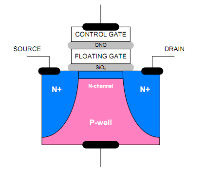
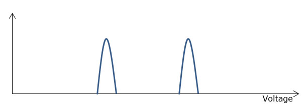
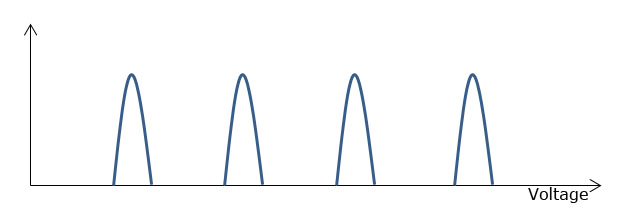
But what does this have to do with SLC, MLC and TLC? The actual MOSFET is exactly the same in all three cases, but take a look at the table below.
| SLC | "0" | High Voltage |
| "1" | Low Voltage | |
| MLC | "00" | High Voltage |
| "01" | Med-High Voltage | |
| "10" | Med-Low Voltage | |
| "11" | Low Voltage | |
| TLC | "000" | Highest Voltage |
| "001" | High Voltage | |
| "010" | Med-High Voltage | |
| "100" | High-Medium Voltage | |
| "011" | Low-Medium Voltage | |
| "101" | Med-Low Voltage | |
| "110" | Low Voltage | |
| "111" | Lowest Voltage |
SLC
MLC
TLC
SLC only has two program states, "0" and "1". Hence either a high or low voltage is required. When the amount of bits goes up, you need more voltage stages. With MLC, there are four states, and eight states with TLC. The problem is that the silicon oxide layer is only about 10nm thick and it's not immortal; it wears out every time it's used in the tunneling process. When the silicon oxide layer wears out, the atomic bonds break and during the tunneling process, some electrons may get trapped inside the silicon oxide. This builds up negative charge in the silicon oxide, which negates some of the the control gate voltage.
At first, erasing becomes slower because higher voltages need to be applied (and for a longer time) before the right voltage is found. Higher voltage causes more stress on the oxide, wearing it out even more. Eventually, erasing will take so long that the block has to be retired to maintain the performance. There is a side effect, though. Programming will be faster because there is already some voltage in the cell due to the electron trapping. However, the time won because of that is much smaller than the time it takes to erase the cell when more voltage pulses are required to erase the cell. That's why the block has to be retired when the wear level reaches a certain point.
Here comes the differerence between SLC, MLC and TLC. The fewer bits you have per cell, the more voltage room you have. In other words, SLC can tolerate more changes in the voltage states because it has only two states. In TLC, there are eight, so the margin for errors is a lot smaller.
Lets assume that we have an SLC NAND that takes voltage between 0V and 14V. To program the cell to "1", a voltage between 4V and 5V needs to be applied. Likewise, you need a voltage from 9V to 10V to program the cell to "0". In this scenario, there is 4V of "spare" voltage between the states. If we apply this example to MLC NAND, the spare voltage will be cut to half, 2V. With TLC, that spare value is only 0.67V if we use the same 1V per voltage state ideaology.
However, when the oxide wears out and a higher voltage is needed, the programming voltages go up. To use the SLC example above, you would now need a voltage between 4V and 6V to program the cell to "0". That means a 1V loss in the spare voltage. And here comes the difference. Since SLC has more spare voltage between the states, it can tolerate a higher voltage change until the erase will be so slow that the block needs to be retired. This is why SLC has a substantially higher P/E cycle count; you can erase and reprogram the cell more times. Likewise, TLC tolerates the least change in voltage states, so it has the lowest amount of P/E cycles.


90 Comments
View All Comments
Kougar - Thursday, February 23, 2012 - link
First, thanks for the article! However it has reignited a question I've had for some time.How is this regulated exactly... does the manufacturer still set a mandatory limit to the number or writes, or is a modern SSD capable of detecting this delay and automatically correcting for it up until the point that it is able to detect the block has exceeded the time limits (and hence write endurance) allowed? In another manner of phrasing it, are arbitrary write count limits utilized or is a modern SSD self-aware enough to determine on its own when a flash block needs to be retired, regardless of the write counts?
Kristian Vättö - Friday, February 24, 2012 - link
Each chip is slightly different so there is no set maximum of writes. One can last 3000 P/E cycles while the other can last 3200.I'm not 100% sure but I think the controller is the one who decides when a certain block is too slow. I.e. it's capable of detecting the delay and when it reaches a certain point, it decides to retire the block to avoid further performance decrease. Hence it may be controller specific and some will retire blocks sooner than others, although at least Intel is saying that there is a certain delay and after that the block is retired (but it may just be a recommendation).
Kougar - Friday, February 24, 2012 - link
Thank you for your reply, Kristian!When you mention every chip is different, that's a very excellent point and one of several reasons for the question.
The other reason behind my question was simply SSD lifespan... Anand has (several times) mentioned that even after the NAND "wears out" the data should remain readable for at least one year after that date.
Yet, all the SSD failures a huge number of others (including myself) have experienced has always been from an SSD suddenly failing outright, and not even being detected in the BIOS. I've yet to come across anyone that's claiming their drive became read only, or something else other than an outright failure or firmware related bug.Basically it seems like SSDs don't wear out, they just completely die outright for some reason. Going by your answer to my question, I'm going to safely assume NAND longevity isn't the factor in these episodes, but any input you may have on this would be quite welcome!
Kristian Vättö - Friday, February 24, 2012 - link
It's true that NAND remains readable when it wears out. For MLC, the period is about one year (eMLC is only 3 months, though).I can't say for sure what is the reason behind these early failures but I would claim that it's often controller related. In general, drives equipped with SandForce controllers experience more early failures than other drives (see the link below).
http://www.behardware.com/articles/843-7/component...
All the drives with +5% return rate are SandForce based, more specifically SF-1222 based. NewEgg yields similar data. SF-2281 based SSDs have quite a few one-star ratings, usually around 20%. Switch to Crucial or Intel (or any other non-SF drive) and we are looking at less than 10% one-star ratings, which usually imply a dead drive.
Of course, even non-SF drives experience early failures but the rate is much smaller and more common for consumer electronics. In any case, it's not the NAND that is causing the failure :-)
Sivar - Thursday, February 23, 2012 - link
I understand the necessity of reducing cost, but a sharp drop in durability coupled with a rapidly diminishing return on $savings/capacity due to the necessary greater redundancy seems a high price to pay for a linear increase in capacity.This is one of those articles that has the excellent writing and technical thoroughness characteristic of something written by Anand himself. To top it off, it doesn't use an inefficient image format for the photos with large areas of flat color, like the first image.
themossie - Friday, February 24, 2012 - link
Second that. Unusual clarity for any technical explanation. Thank you for the article, Kristian!hechacker1 - Friday, February 24, 2012 - link
I think the article got confusing by adding that that you can use less flash at 10.67Gb, along with 3bits per cell, giving 32Gb. Do the math: 10.67Gb * 3bits per cell = 32Gb.It's easier to just keep in mind:
16Gb NAND * 1 bit per cell = 16Gb capacity
16Gb NAND * 2 bit per cell = 32Gb capacity
16Gb NAND * 3 bit per cell = 48Gb capacity
Kristian Vättö - Friday, February 24, 2012 - link
The reason is that no final product has capacity of 48Gb. Capacities go in powers of 2: 2Gb, 4Gb, 8Gb, 16Gb, 32Gb, 64Gb and so on. 48Gb isn't a power of two (and no X*3 is). Hence you have to make the die smaller so that the X*3 is a power of two, like 10.67Gb is.In theory, you could make a 48Gb TLC die and it would work just fine. It's simply considered as an odd number in the NAND industry and hence not used.
themossie - Friday, February 24, 2012 - link
Kristian says this is awkward because TLC capacities will not scale from MLC capacities at a power of 2, like MLC did from SLC. I am not convinced that's an issue, as scaling capacity by a power of 2 has never been a requirement in the hard drive industry.Indeed, 80/90 GB SSDs - located between power-of-2-inspired 64 GB and 128 GB capacities - have been quite popular. For that matter, 64GB/128GB SSDs are often marketed as 60GB/120GB SSDs, partially due to provisioning...
It is awkward to describe 48Gb as 10.67Gb*3, where Gb represents physical transistors rather than bits; Gb is a unit for digital information in this context, not the physical representation of such.
This is exacerbated as the cells are physically identical - an array could store 48Gb using TLC, but only 10.67Gb with SLC. I find hechacker1's explanation more intuitive. 16Gb SLC = (16*2) 32Gb MLC = (16*3) 48Gb TLC...
The takeaway point here is that you get 50% more wafers per die for a given capacity with TLC over MLC, and this shows up directly in the cost ($0.60 cents/gb vs $0.90 cents/gb) but results in greatly reduced write cycles.
Kristian Vättö - Friday, February 24, 2012 - link
Remember that I'm not the one who came up with this idea ;-)This info is straight from Micron and they indeed say that the TLC die is chopped down to 10.67 billion transistors so that it becomes a 32Gb die. Maybe OEMs are afraid of adapting "odd number" capacities. In SSDs it wouldn't be so big deal but TLC is more commonly used in devices like USB flash drives and low-end smartphones. In fact, some OEMs may even use MLC and TLC in the same model (I don't have any examples but I wouldn't be surprised).
As for why some drives have an odd capacity, it has to do with the controller design and over-provisioning. Intel's SATA 3Gb/s controller has 10 channels while most controllers have 8. That's why Intel drives have weird capacities. Populate all 10 channels with 64Gb (8GB) dies and you get 80GB. For other drives, populating all the channels works out to be only 64GB. As for SandForce drives, they have no on-board cache (DRAM) so some of the NAND (~7%) is preserved for that. That's why 128GB SF drive is marketed as 120GB.
I agree that 10.67 is an awkward number but then again, this is stuff that an average consumer doesn't really need to know. For them, the final product will look the same, thanks to the power of two capacity. The gain of TLC is the same, no matter is the die smaller or the same as MLC. TLC provides more GB per die, which means cheaper $/GB.