Samsung Details Exynos 5 Octa Architecture & Power at ISSCC '13
by Anand Lal Shimpi on February 20, 2013 12:42 PM EST- Posted in
- SoCs
- Samsung
- Arm
- Cortex A15
- Cortex A7
- exynos 5 octa
At CES this year Samsung introduced the oddly named Exynos 5 Octa SoC, one of the first Cortex A15 SoCs to implement ARM's big.LITTLE architecture. Widely expected to be used in the upcoming Galaxy S 4, the Exynos 5 Octa integrates 4 ARM Cortex A7 cores and 4 ARM Cortex A15 cores on a single 28nm LP HK+MG die made at Samsung's own foundry. As we later discovered, the Exynos 5 Octa abandons ARM's Mali GPU for Imagination's PowerVR SGX 544MP3, which should give it GPU performance somewhere between an iPad 3 and iPad 4.
The quad-core A7 can run at between 200MHz and 1.2GHz, while the quad-core A15 can run at a range of 200MHz to 1.8GHz. Each core can be power gated independently. The idea is that most workloads will run on the quad-core A7, with your OS hot plugging additional cores as performance demands increase. After a certain point however, the platform will power down the A7s and start switching over to the A15s. Both SoCs implement the same revision of the ARM ISA, enabling seamless switching between cores. While it's possible for you to use both in parallel, initial software implementations will likely just allow you to run on the A7 or A15 clusters and switch based on performance requirements.
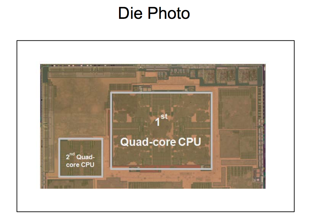
What's most interesting about Samsung's ISSCC presentation is we finally have some hard power and area data comparing the Cortex A15 to the Cortex A7. The table above puts it into numbers. The quad-core A15 cluster occupies 5x the area of the quad-core A7 cluster, and consumes nearly 6x the power in the worst case scenario. The area difference is artificially inflated by the fact that the A15 cluster has an L2 cache that's 4x the size of the A7 cluster, but looking at the die photo below you can get a good feel for just how much bigger the A15 cores are themselves:
In its ISSCC presentation, Samsung stressed the value of its custom libraries, timing tweaks and process technology selection in bringing the Exynos 5 Octa to market. Samsung is definitely marching towards being a real player in the SoC space and not just another ARM licensee.
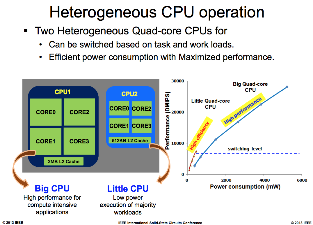
The chart below is one of the most interesting, it shows the relationship between small integer code performance and power consumption on the Cortex A7 and A15 clusters. Before switching from the little CPU to the big one, power consumption is actually quite reasonable - south of 1W and what you'd expect for a smartphone or low power tablet SoC. At the lower end of the performance curve for the big CPU things aren't too bad either, but once you start ramping up clock speed and core count power scales linearly. Based on this graph, it looks like it takes more than 3x the power to get 2x the performance of the A7 cluster using the Cortex A15s.


52 Comments
View All Comments
Cow86 - Thursday, February 21, 2013 - link
Because the A7 is specifically designed to be a Little core to the A15. The A5 is not. Furthermore the A7 has a better performance/watt than the A5, and a very similar die size.saurabhr8here - Wednesday, February 20, 2013 - link
Both say ARM v7a, which is the instruction set architecture. Both A7 and A15 processors use the same instruction set, hence they are able to implement the big.LITTLE architecture in the first place.twotwotwo - Wednesday, February 20, 2013 - link
Nah, it's talking about the instruction set. v7a is the common instruction set for the A7 and A15 microarchitectures.MrSpadge - Wednesday, February 20, 2013 - link
The Architecture is Arm v7a, the actual chip designs are called A7 and A15. This means both designs understand the same instructions and can thus run the same software (which is needed for quick transparent switches). ARM is not very good at the naming game yet.SetiroN - Wednesday, February 20, 2013 - link
It can be misleading if you don't pay attention, ARM v7a is the architecture revision (ISA), Cortex A15 and A7 are the core's names, which aren't mentioned on that chart.toyotabedzrock - Wednesday, February 20, 2013 - link
I have to wonder if they tested the a7 to ensure it has the power to run the ui smoothly.UpSpin - Wednesday, February 20, 2013 - link
No, they never test it. They haven't even tested if the SoC works at all. And the performance numbers, they are just random numbers. /sThe A7 is only slightly slower than an A9. Android JB runs smooth on dual core A9 SoCs because it makes heavy use of the GPU for rendering. So for lag free UI the GPU will be more important.
A quad core A7 will be faster than a A9 dual core! It will handle the usual tasks without any issues at all.
tuxRoller - Thursday, February 21, 2013 - link
http://www.arm.com/products/processors/cortex-a/co...They're claiming around a 20% improvement, but I'm guessing that's at the high end. Other numbers I've seen claim it to be a bit below an A8.
However, it uses MUCH less power than these other chips (arm claim it's similar to an A5 in terms of power draw).
Considering it looks as though the biggest change (to the A8) is in the branch prediction, and it should clock higher,
http://www.arm.com/products/processors/cortex-a/co...
phoenix_rizzen - Wednesday, February 20, 2013 - link
The A7 is supposed to have just slightly less performance than an A9, but with much reduced power requirements. It will most likely take over from the A8 and low-end A9 SoCs for low-to-middle-range phones. Look for dual-core A7s to hit "feature" phones this year.MrSpadge - Wednesday, February 20, 2013 - link
Looks like sharing the L2 between both CPU clusters might be a good idea. Done in some clever way it could even speed the switching up.