AMD’s Kaveri: Pre-Launch Information
by Ian Cutress on January 6, 2014 8:00 PM EST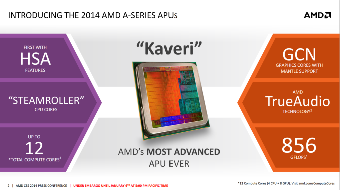
On the back of AMD’s Tech Day at CES 2014, all of which was under NDA until the launch of Kaveri, AMD have supplied us with some information that we can talk about today. For those not following the AMD roadmap, Kaveri is the natural progression of the AMD A-Series APU line, from Llano, Trinity to Richland and now Kaveri. At the heart of the AMD APU design is the combination of CPU cores (‘Bulldozer’, ‘Steamroller’) and a large dollop of GPU cores for on-chip graphics prowess.
Kaveri is that next iteration in line which uses an updated FM2+ socket from Richland and the architecture is updated for Q1 2014. AMD are attacking with Kaveri on four fronts:
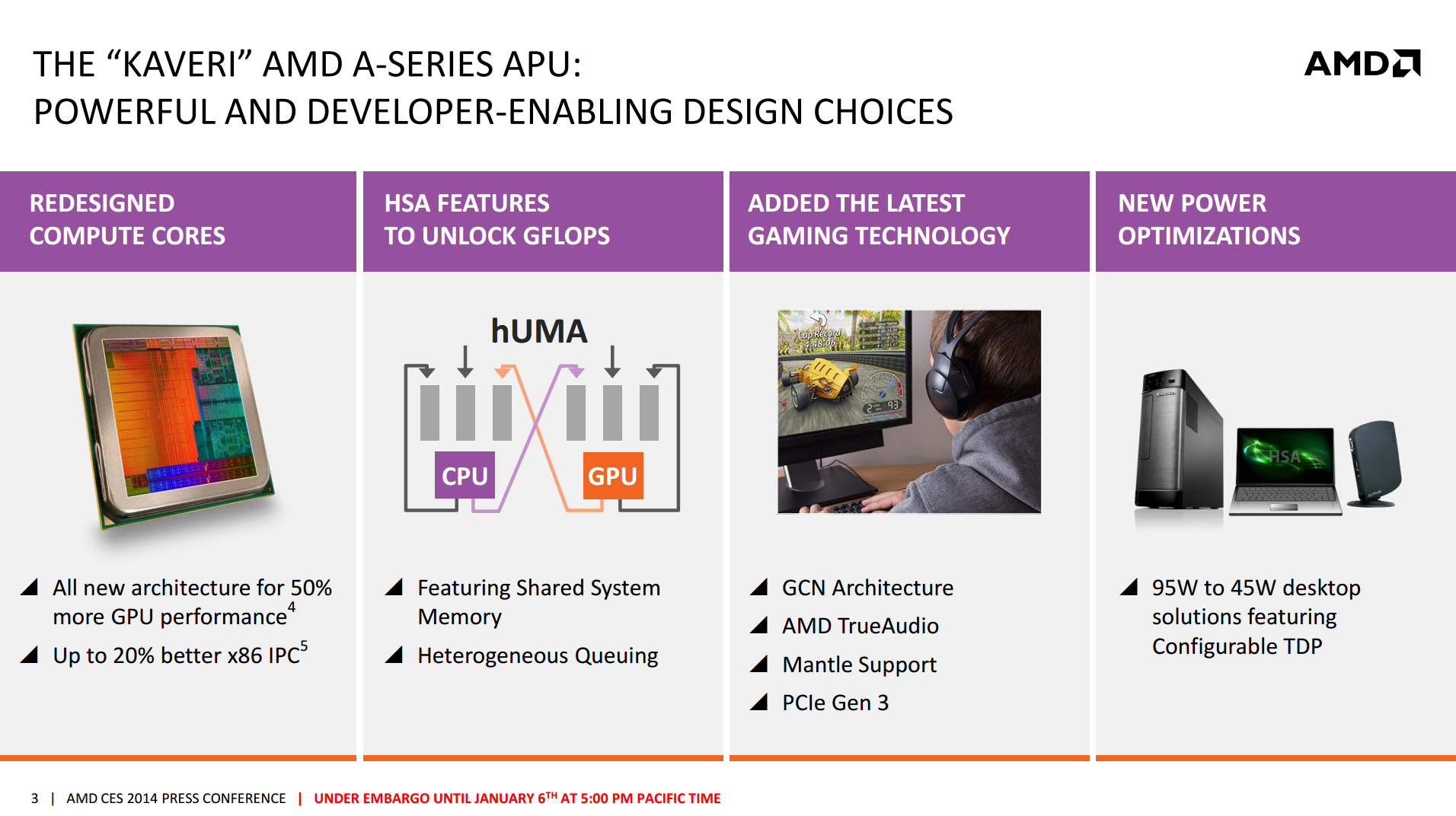
Redesigned Compute Cores* (Compute = CPU + GPU)
Kaveri uses an enhanced version of the Richland CPU core, codename Steamroller. As with every new CPU generation or architecture update, the main goal is better performance and lower power – preferably both. AMD is quoting a 20% better x86 IPC with Kaveri compared to Richland when put clock to clock. For the purposes of this information release, we were provided with several AMD benchmarking results to share:
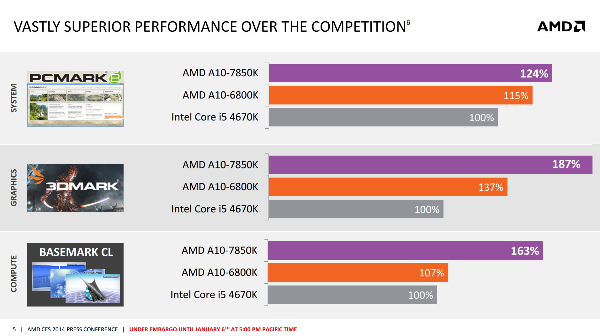
These results border pretty much on the synthetic – AMD did not give any real world examples today but numbers will come through in time. AMD is set to release two CPUs on January 14th (date provided in our pre-release slide deck), namely the A10-7700K and the A10-7850K. Some of the specifications were also provided:
| AMD APUs | ||||
|
Richland A8-6600K |
Richland A10-6800K |
Kaveri A10-7700K |
Kaveri A10-7850K |
|
| Release | June 4 '13 | June 4 '13 | Jan 14th '14 | Jan 14th '14 |
| Frequency | 3900 MHz | 4100 MHz | ? | 3700 MHz |
| Turbo | 4200 MHz | 4400 MHz | ? | ? |
| DRAM | DDR3-1866 | DDR3-2133 | DDR3-2133 | DDR3-2133 |
| Microarhitecture | Piledriver | Piledriver | Steamroller | Steamroller |
| Manufacturing Process | 32nm | 32nm | ? | ? |
| Modules | 2 | 2 | ? | 2 |
| Threads | 4 | 4 | ? | 4 |
| Socket | FM2 | FM2 | FM2+ | FM2+ |
| L1 Cache |
2 x 64 KB I$ 4 x 16 KB D$ |
2 x 64 KB I$ 4 x 16 KB D$ |
? | ? |
| L2 Cache | 2 x 2 MB | 2 x 2 MB | ? | ? |
| Integrated GPU | HD 8570D | HD 8670D | R7 | R7 |
| IGP Cores | 256 | 384 | ? | 512 |
| IGP Architecture | Cayman | Cayman | GCN | GCN |
| IGP Frequency | 844 | 844 | ? | 720 |
| Power | 100W | 100W | ? | 95W |
All the values marked ‘?’ have not been confirmed at this point, although it is interesting to see that the CPU MHz has decreased from Richland. A lot of the APU die goes to that integrated GPU, which as we can see above becomes fully GCN, rather than the Cayman derived Richland APUs. This comes with a core bump as well, seeing 512 GPU cores on the high end module – this equates to 8 CUs on die and what AMD calls ’12 Compute Cores’ overall. These GCN cores are primed and AMD Mantle ready, suggesting that performance gains could be had directly from Mantle enabled titles.
Described in AMD’s own words: ‘A compute core is an HSA-enabled hardware block that is programmable (CPU, GPU or other processing element), capable of running at least one process in its own context and virtual memory space, independently from other cores. A GPU Core is a GCN-based hardware block containing a dedicated scheduler that feeds four 16-wide SIMD vector processors, a scalar processor, local data registers and data share memory, a branch & message processor, 16 texture fetch or load/store units, four texture filter units, and a texture cache. A GPU Core can independently execute work-groups consisting of 64 work items in parallel.’ This suggests that if we were to run asynchronous kernels on the AMD APU, we could technically run twelve on the high end APU, given that each Compute Core is capable of running at least one process in its own context and virtual memory space independent of the others.
The reason why AMD calls them Compute Cores is based on their second of their four pronged attack: hUMA.
HSA, hUMA, and all that jazz
AMD went for the heterogeneous system architecture early on to exploit the fact that many compute intensive tasks can be offloaded to parts of the CPU that are designed to run them faster or at low power. By combining CPU and GPU on a single die, the system should be able to shift work around to complete the process quicker. When this was first envisaged, AMD had two issues: lack of software out in the public domain to take advantage (as is any new computing paradigm) and restrictive OS support. Now that Windows 8 is built to allow HSA to take advantage of this, all that leaves is the programming. However AMD have gone one step further with hUMA, and giving the system access to all the memory, all of the time, from any location:
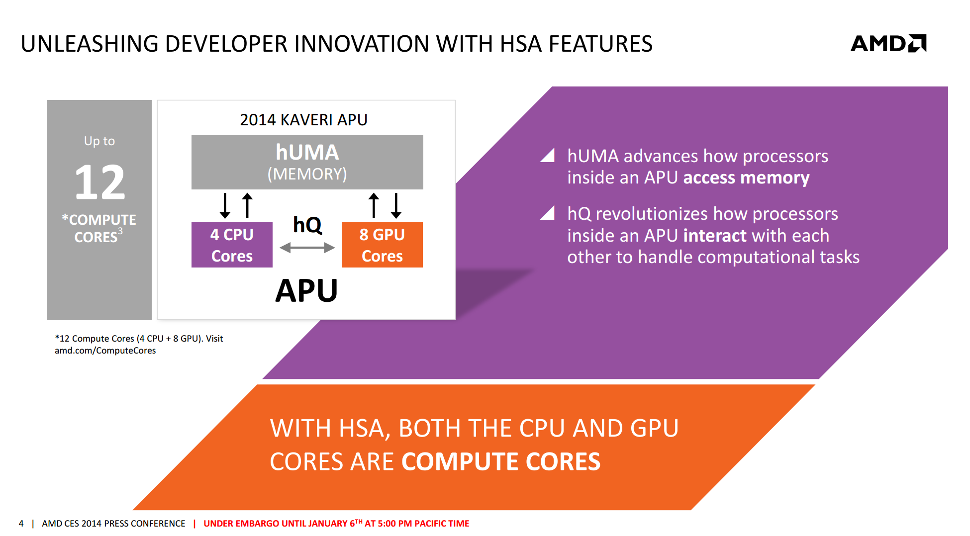
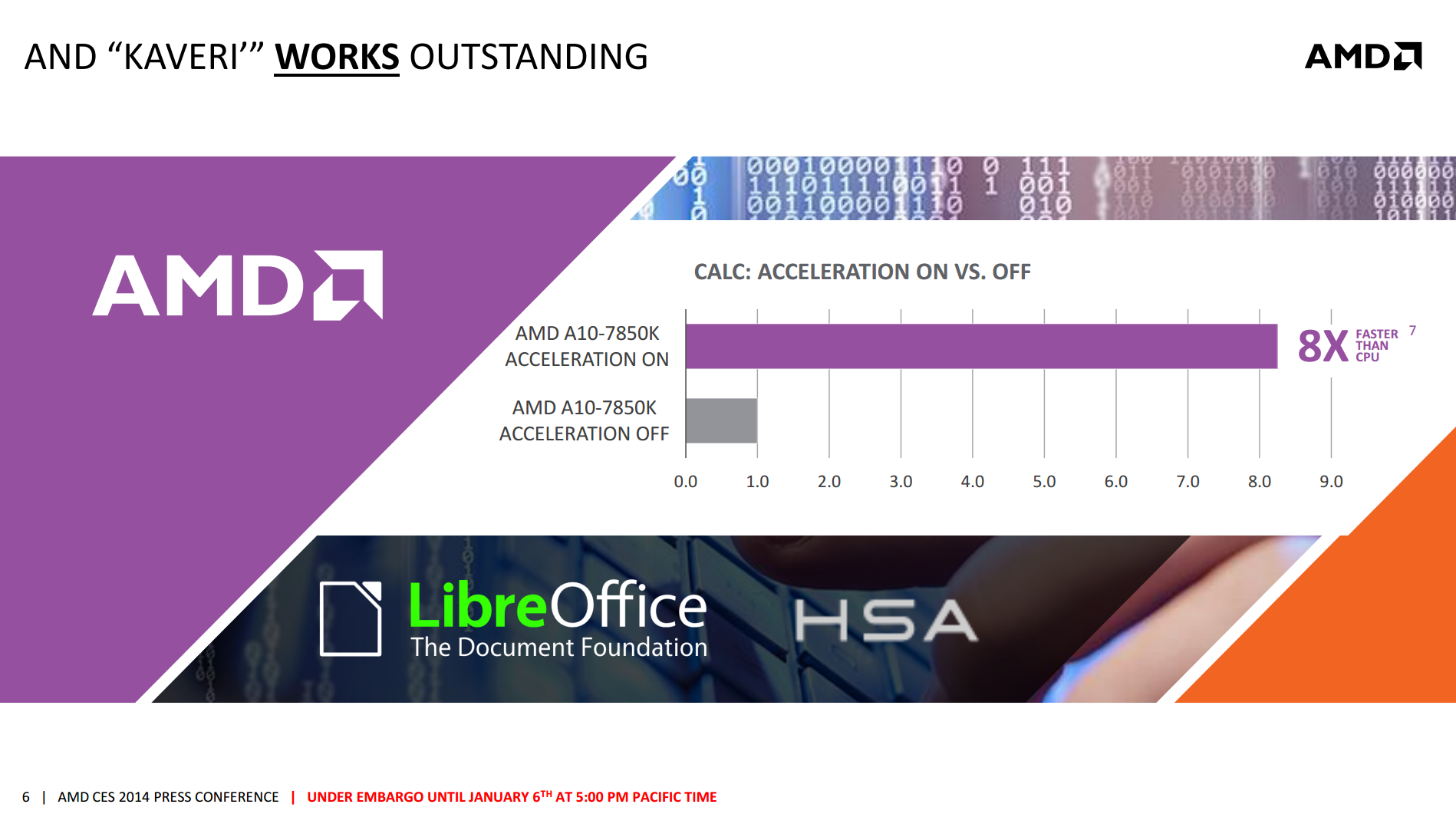
Now that Kaveri offers a proper HSA stack, and can call upon 12 compute cores to do work, applications that are designed (or have code paths) to take advantage of this should emerge. One such example that AMD are willing to share today is stock calculation using LibreOffice's Calc application – calculating the BETA (return) of 21 fake stocks and plotting 100 points on a graph of each stock. With HSA acceleration on, the system performed the task in 0.12 seconds, compared to 0.99 seconds when turned off.
Prong 3: Gaming Technologies
In a year where new gaming technologies are at the forefront of design, along with gaming power, AMD are tackling the issue on one front with Kaveri. By giving it a GCN graphics backbone, features from the main GPU line can fully integrate (with HSA) into the APU. As we have seen in previous AMD releases and talks, this means several things:
- Mantle
- AMD TrueAudio
- PCIe Gen 3
AMD is wanting to revolutionize the way that games are played and shown with Mantle – it is a small shame that the Mantle release was delayed and that AMD did not provide any numbers to share with us today. The results should find their way online after release however.
Prong 4: Power Optimisations
With Richland we had CPUs in the range of 65W to 100W, and using the architecture in the FX range produced CPUs up to 220W. Techincally we had 45W Richland APUs launch, but to date I have not seen one for sale. However this time around, AMD are focusing a slightly lower power segment – 45W to 95W. Chances are the top end APUs (A10-7850K) will be 95W, suggesting that we have a combination of a 20% IPC improvement, 400 MHz decrease but a 5% TDP decrease for the high end chip. Bundle in some HSA and let’s get this thing on the road.
Release Date
AMD have given us the release date for the APUs: January 14th will see the launch of the A10-7850K and the A10-7700K. Certain system builders should be offering pre-built systems based on these APUs from today as well.


133 Comments
View All Comments
KenLuskin - Sunday, January 12, 2014 - link
Do you understand that supercomputers use GPU acceleration chips?WHY?
For the same reason that Servers will employ AMD APUs.
Maybe you need a remedial course about APUs?
I suggest these 2 videos:
1) Revolutionizing computing with HSA-enabled APU
http://www.youtube.com/watch?v=4YV6z6Fgw48
2) "Your processor's IQ: An Intro to HSA"
http://www.youtube.com/watch?v=i6BWzL12KMI
BMNify - Monday, January 13, 2014 - link
"FlanK3r: Do you understand that supercomputers use GPU acceleration chips?WHY?
For the same reason that Servers will employ AMD APUs.
Maybe you need a remedial course about APUs? ...
...Revolutionizing computing with HSA-enabled APU"
wow there dobbin http://i1.trekearth.com/photos/348/dobbin_smiles_m...
your logic is Non sequitur ((Latin for "it does not follow"), in formal logic, is an argument in which its conclusion does not follow from its premises.)
first of all they call Graphic Processing Unit's specialized Co-Processors for a reason...
in that they are specially constructed to perform lots of compute intensive thread-able tasksfor algorithms where processing of large blocks of data that can be done in parallel.
for instance Released in 1985, the Commodore Amiga was one of the first personal computers to come standard with a GPU. The GPU supported line draw, area fill, and included a type of stream processor called a blitter which accelerated the movement, manipulation, and combination of multiple arbitrary bitmaps. Also included was a coprocessor with its own (primitive) instruction set capable of directly invoking a sequence of graphics operations without CPU intervention.
it also had a Heterogeneous System Architecture in that it had "Chip RAM" that was shared between the central processing unit (CPU) and the dedicated chipset co-processors Agnus (DMA) controller (hence the name).
Agnus operates a system where the "odd" clock cycle is allocated to time-critical custom chip access and the "even" cycle is allocated to the CPU, thus the CPU is not typically blocked from memory access and may run without interruption. However, certain chipset DMA, such as copper or blitter operations, can use any spare cycles, effectively blocking cycles from the CPU. In such situations CPU cycles are only blocked while accessing shared RAM, but never when accessing external RAM or ROM
Prior to this and for quite some time after, many other personal computer systems instead used their main, general-purpose CPU to handle almost every aspect of drawing the display, short of generating the final video signal...
moving on to today, in your average so called supercomputer gpu-compute intensive tasks/functions take up around 5% of the total time of a given app where the rest are sequential SIMD code usually.... http://www.nvidia.com/docs/IO/143716/how-gpu-accel...
of all these supercomputer gpu-compute intensive tasks how many will you be running on your home/SOHO Heterogeneous System Architecture Soc exactly, http://www.nvidia.com/content/tesla/pdf/gpu-apps-c...
none would be a fair guess....
you don't really believe this AMD PR "processor's IQ" do you , ,here's a hint, processors do not have any IQ , the worlds best engineers cant even simulate cognitive responses in real time yet never mind simulated IQ....
and for fun here's a little demo to show how a specialist gfx Co-Processor is good at fast gfx manipulation and not much else as it does not have a high sequential integer SIMD capability on a very high data interconnect such as todays CPU's and their AVX2 SIMD for instance.
https://www.youtube.com/watch?v=-P28LKWTzrI
BMNify - Monday, January 13, 2014 - link
oops bad copy paste there , i OC mean Ken Luskin saidravyne - Monday, January 6, 2014 - link
There's actually quite a number of applications which are bottle-necked both by the limited parallel throughput of CPUs (even with SSE and AVX) and by the latency / overhead of moving smaller amounts of data over the PCIe bus. Those applications will benefit enormously from having access to what's effectively a smaller, but practically latency-free GPU.inighthawki - Monday, January 6, 2014 - link
Go check out Microsoft's C++ AMP library. C++-like semantics but all Direct Compute under the hood. The dev cost is minimal if the performance is worth it.nico_mach - Wednesday, January 8, 2014 - link
More importantly, if these are games/ apps already written for xbox one/ps4, the porting time could be minimal.duploxxx - Tuesday, January 7, 2014 - link
depends on who actually is interested. just lok at following announcement:http://www.javaworld.com/article/2078856/mobile-ja...
if java source code is optimised, how many do you think just use java do write applications....
tcube - Tuesday, January 7, 2014 - link
many! Boatloads of huge business softwares are written in pure java...Megatomic - Tuesday, January 7, 2014 - link
We use Java extensively in our data acquisition systems. Java is far more pervasive than many would believe.mikato - Wednesday, January 8, 2014 - link
HSA exploitation in Java would be huge!Also, there are plenty of places where it would be a big advantage to a company to enable big performance improvements with some resources spent developing the ability to use HSA. It's a direct competitive advantage in certain situations.