Intel Reveals New Haswell Details at ISSCC 2014
by Anand Lal Shimpi on February 9, 2014 3:00 PM EST- Posted in
- CPUs
- Intel
- Haswell
- ISSCC
- ISSCC 2014
As of late, Intel has been unusually guarded about releasing information about its microprocessor designs. Haswell launched last year with great architecture disclosure, but very limited disclosure about die sizes, transistor counts and almost anything surrounding the interface between Haswell and its optional embedded DRAM (Crystalwell) counterpart. This week at ISSCC, Intel will finally be filling in some of the blanks.
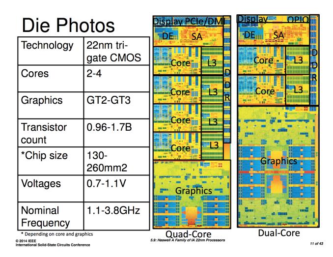
The first bit of new information we have are official transistor counts for the range of Haswell designs. At launch Intel only disclosed transistor counts and die areas for Haswell ULT GT3 (dual-core, on-die PCH, GT3 graphics) and Haswell GT2 (quad-core, no on-die PCH, GT2 graphics). Today we have both the minimum and maximum configurations for Haswell. Note all transistor counts below are schematic not layout:
| Intel Haswell | |||||||||||||||||
| CPU Configuration | GPU Configuration | Die Size | Transistor Count | ||||||||||||||
| 4+3 | Quad-Core | GT3e | 260mm2 + 77mm2 | 1.7B + ? | |||||||||||||
| ULT 2+3 | Dual-Core | GT3 | 181mm2 | 1.3B | |||||||||||||
| ULT 2+2 | Dual-Core | GT2 | ? | (est) ~1B | |||||||||||||
| 4+2 | Quad-Core | GT2 | 177mm2 | 1.4B | |||||||||||||
| 2+2 | Dual-Core | GT2 | 130mm2 | 0.96B | |||||||||||||
I've organized the table above by decreasing die size. I still don't have confirmation for the ULT 2+2 configuration, but the rest is now filled in and accurate. If you remember back to our Iris Pro review, I measured the die area for Haswell GT3 and the Crystalwell eDRAM using some cheap calipers. I came up with 264mm2 + 84mm2, the actual numbers are pretty close at 260mm2 + 77mm2.
Doing some rough math we see that the addition of a third graphics slice to a Haswell core accounts for around 300M transistors. That would put the ULT2+2 configuration at around 1B total transistors. I suspect the ULT 2+2 configuration is similar in size to the quad-core + GT2 configuration.
Next up on the list is some additional information on the Crystalwell (embedded DRAM) design and configuration. Intel explained how it arrived at the 128MB L4 eDRAM cache size, but it wouldn't tell us the operating frequency of the memory or the interface between it and the main CPU die. In its ISSCC disclosures, Intel filled in the blanks:
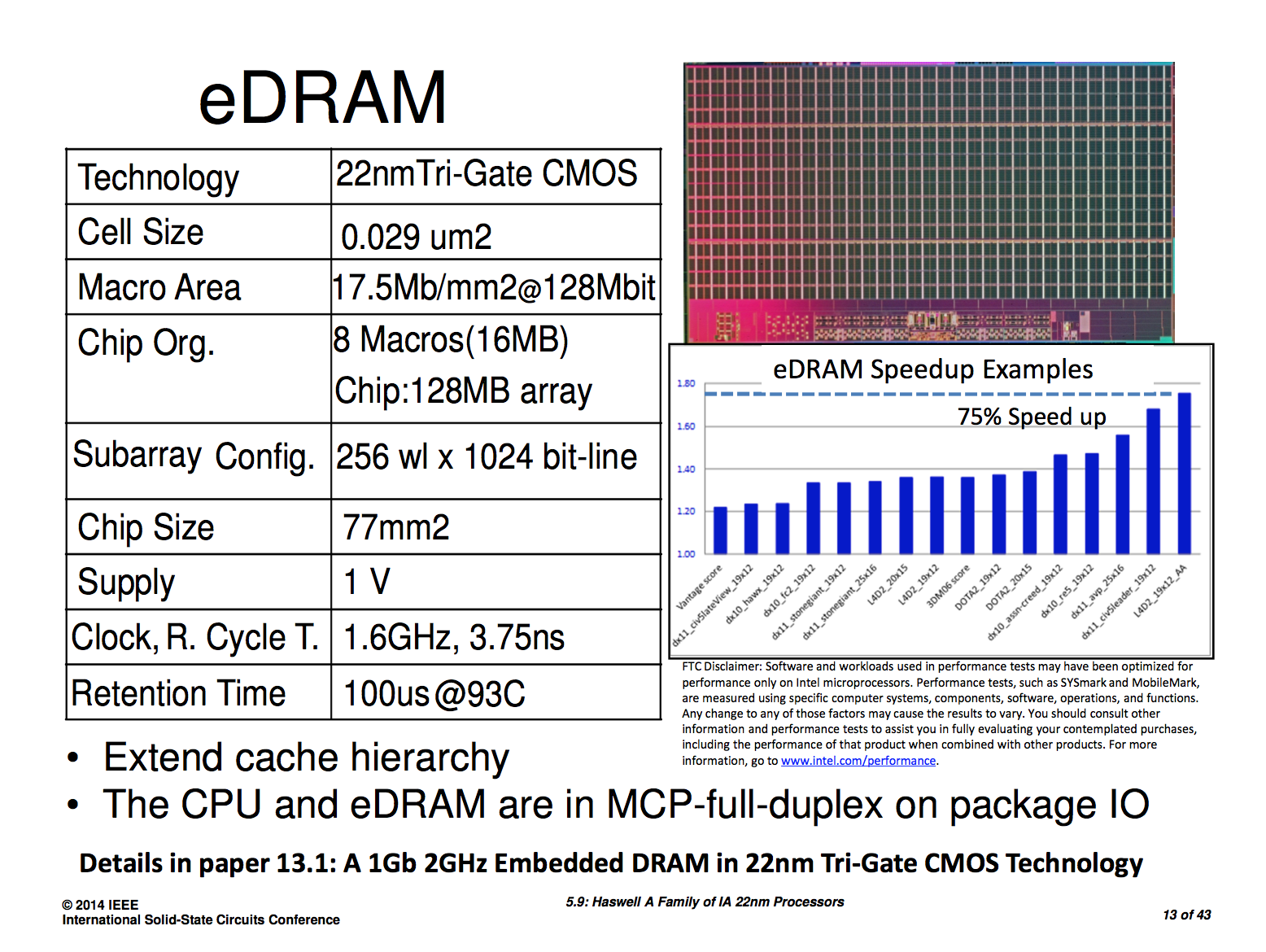
The 128MB eDRAM is divided among eight 16MB macros. The eDRAM operates at 1.6GHz and connects to the outside world via a 4 x 16-bit wide on-package IO (OPIO) interface capable of up to 6.4GT/s. The OPIO is highly scalable and very area/power efficient. The Haswell ULT variants use Intel's on-package IO to connect the CPU/GPU island to an on-package PCH. In this configuration the OPIO delivers 4GB/s of bandwidth at 1pJ/bit. When used as an interface to Crystalwell, the interface delivers up to 102GB/s at 1.22pJ/bit. That amounts to a little under 1.07W of power consumed to transmit/receive data at 102GB/s.
By keeping the eDRAM (or PCH) very close to the CPU island (1.5mm), Intel can make the OPIO extremely simple.
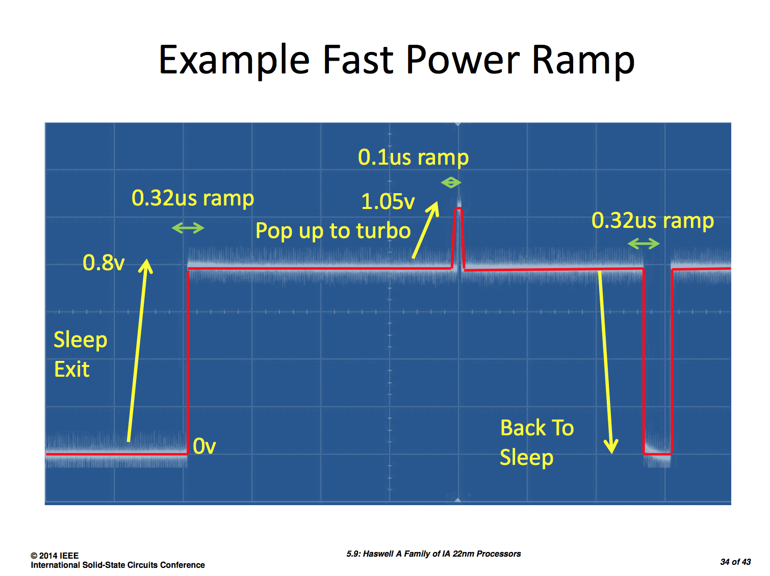
Intel also shared some data on how it achieved substantial power savings with Haswell, including using a new stacked power gate for the memory interface that reduced leakage by 100x over Ivy Bridge. Haswell's FIVR (Full Integrated Voltage Regulator) is also a topic of discussion in Intel's ISSCC papers. FIVR ends up being 90% efficient under load and can enter/exit sleep in 0.32µs, requiring only 0.1µs to ramp up to turbo frequencies.
Intel's Haswell ISSCC disclosures don't really change anything about Haswell, but they do further illustrate just how impressive of a design it is.


44 Comments
View All Comments
iwod - Sunday, February 9, 2014 - link
Are the any news in regards as to why Xeon and all Server chips are always one node behind? And soon the desktop Haswell-Refresh as well? Will Intel simply relegate all Desktop and Server to older nodes while focusing new node development on Ultra Low Power for Laptop and Mobile Devices?fluxtatic - Sunday, February 9, 2014 - link
The Xeon variants remain one node behind due to obligations for extended validation and support of the platforms. Intel can develop a new architecture and get it ready for consumer-level release, making back the R&D money they're putting into it, while they're simultaneously developing, testing, and validating the Xeon variants. It just makes sense to release Xeon on a mature arch (eg, one generation behind), as there is a significant amount of time and money involved getting the current generation behind adapted into the Xeon platform requirements.Lately, Intel is moving in the direction you describe - targeting mobile (well, laptop) processors first, followed by desktop, and then server/workstation. That makes sense, as well, as laptop processor sales are outstripping desktop. As a bit of speculation, it may be easier to target the lowest-power targets first, and scale up, rather than trying to do the reverse.
BMNify - Sunday, February 9, 2014 - link
"The 128MB eDRAM is divided among eight 16MB macros. The eDRAM operates at 1.6GHz and connects to the outside world via a 4 x 16-bit wide on-package IO (OPIO) interface capable of up to 6.4GT/s. The OPIO is highly scalable and very area/power efficient.The Haswell ULT variants use Intel's on-package IO to connect the CPU/GPU island to an on-package PCH. In this configuration the OPIO delivers 4GB/s of bandwidth at 1pJ/bit. When used as an interface to Crystalwell, the interface delivers up to 102GB/s at 1.22pJ/bit. That amounts to a little under 1.07W of power consumed to transmit/receive data at 102GB/s.
By keeping the eDRAM (or PCH) very close to the CPU island (1.5mm), Intel can make the OPIO extremely simple."
hmm anand, care to explain please how and why you state "a 4 x 16-bit wide on-package IO (OPIO) interface capable of up to 6.4GT/s." that's a total of 25.6GB/s (at 4.8GT/s it would provide 19.2GB/s total bandwidth to the processor) and yet you say "the interface delivers up to 102GB/s at 1.22pJ/bit. That amounts to a little under 1.07W of power consumed to transmit/receive data at 102GB/s." implying that it has 4 times the bandwidth in real terms ?
so is the 4 x 16-bit wide being used here to obfuscate the fact its really a max data throughput of 6.4 GBps per link x 4 and so matching the generic Quickpath Interconnect speeds
Stahn Aileron - Monday, February 10, 2014 - link
Some rough math:4 x 16 bit = 8 bytes/transfer.
8 bytes/transfer x 6.4 GT/s = 51.2 GB/s.
So 51.2 GB/s raw bandwidth (no overhead accounted for.) 102 GB/s total throughput as Anand states sounds like the bus is bi-directional with 51.2 GB/s possible in each direction. So 51.2 GB/s x2 (both directions at the same time) give you "up to 102 GB/s" throughput overall.
How did you arrive at the 25.6 GB/s value originally?
DanNeely - Monday, February 10, 2014 - link
The 102.5 number appears to come from Intel slide #16 (AT gallery #6). That slide says there are 8 data clusters operating at 6.4GB/s each, with the final x2 apparently being from the bus supporting simultaneous transfer in each direction.twotwotwo - Sunday, February 9, 2014 - link
I'm sorta curious about the potential for CRW, or some future version of it, for CPU performance.More-dynamic programming languages tend to have largish working sets and lots of indirection. In general,the processor still stalls waiting on RAM a lot across lots of workloads. Maybe an "L4" could be a nontrivial win for server-y workloads if the latency/size were right and they shipped it for servers. It's hard to tell; the fact that they're not talking about CRW as a CPU boost does say something.
zodiacfml - Monday, February 10, 2014 - link
I still haven't seen benchmarks whether or not the eDRAM contributes on improving some application performance...or did I missed it?twotwotwo - Monday, February 10, 2014 - link
I'd love info on this, too. I just poked around in the big list at http://www.cpubenchmark.net/high_end_cpus.html and did see this:Intel Core i7-4960HQ @ 2.60GHz (6M L3, CRW) 10,325
Intel Core i7-4900MQ @ 2.80GHz (8M L3) 9,123
If I'm reading it right, the part with CRW (the eDRAM package) did tennish percent better despite lower nominal clock and less L3, on something presented as a pure CPU benchmark. So it did something.
But someone who knows what they're doing could dig into whether that impression is right, and what sort of app sees the biggest gains.
toyotabedzrock - Monday, February 10, 2014 - link
Your die size for the ult 2+2 is way higher than it should be. There is no reason it would be much bigger than the 2+2.TiGr1982 - Monday, February 10, 2014 - link
Indeed, 140-160 mm^2 should be the case for ULT 2+2, not 180 mm^2.