Intel Reveals New Haswell Details at ISSCC 2014
by Anand Lal Shimpi on February 9, 2014 3:00 PM EST- Posted in
- CPUs
- Intel
- Haswell
- ISSCC
- ISSCC 2014
As of late, Intel has been unusually guarded about releasing information about its microprocessor designs. Haswell launched last year with great architecture disclosure, but very limited disclosure about die sizes, transistor counts and almost anything surrounding the interface between Haswell and its optional embedded DRAM (Crystalwell) counterpart. This week at ISSCC, Intel will finally be filling in some of the blanks.
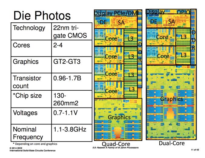
The first bit of new information we have are official transistor counts for the range of Haswell designs. At launch Intel only disclosed transistor counts and die areas for Haswell ULT GT3 (dual-core, on-die PCH, GT3 graphics) and Haswell GT2 (quad-core, no on-die PCH, GT2 graphics). Today we have both the minimum and maximum configurations for Haswell. Note all transistor counts below are schematic not layout:
| Intel Haswell | |||||||||||||||||
| CPU Configuration | GPU Configuration | Die Size | Transistor Count | ||||||||||||||
| 4+3 | Quad-Core | GT3e | 260mm2 + 77mm2 | 1.7B + ? | |||||||||||||
| ULT 2+3 | Dual-Core | GT3 | 181mm2 | 1.3B | |||||||||||||
| ULT 2+2 | Dual-Core | GT2 | ? | (est) ~1B | |||||||||||||
| 4+2 | Quad-Core | GT2 | 177mm2 | 1.4B | |||||||||||||
| 2+2 | Dual-Core | GT2 | 130mm2 | 0.96B | |||||||||||||
I've organized the table above by decreasing die size. I still don't have confirmation for the ULT 2+2 configuration, but the rest is now filled in and accurate. If you remember back to our Iris Pro review, I measured the die area for Haswell GT3 and the Crystalwell eDRAM using some cheap calipers. I came up with 264mm2 + 84mm2, the actual numbers are pretty close at 260mm2 + 77mm2.
Doing some rough math we see that the addition of a third graphics slice to a Haswell core accounts for around 300M transistors. That would put the ULT2+2 configuration at around 1B total transistors. I suspect the ULT 2+2 configuration is similar in size to the quad-core + GT2 configuration.
Next up on the list is some additional information on the Crystalwell (embedded DRAM) design and configuration. Intel explained how it arrived at the 128MB L4 eDRAM cache size, but it wouldn't tell us the operating frequency of the memory or the interface between it and the main CPU die. In its ISSCC disclosures, Intel filled in the blanks:
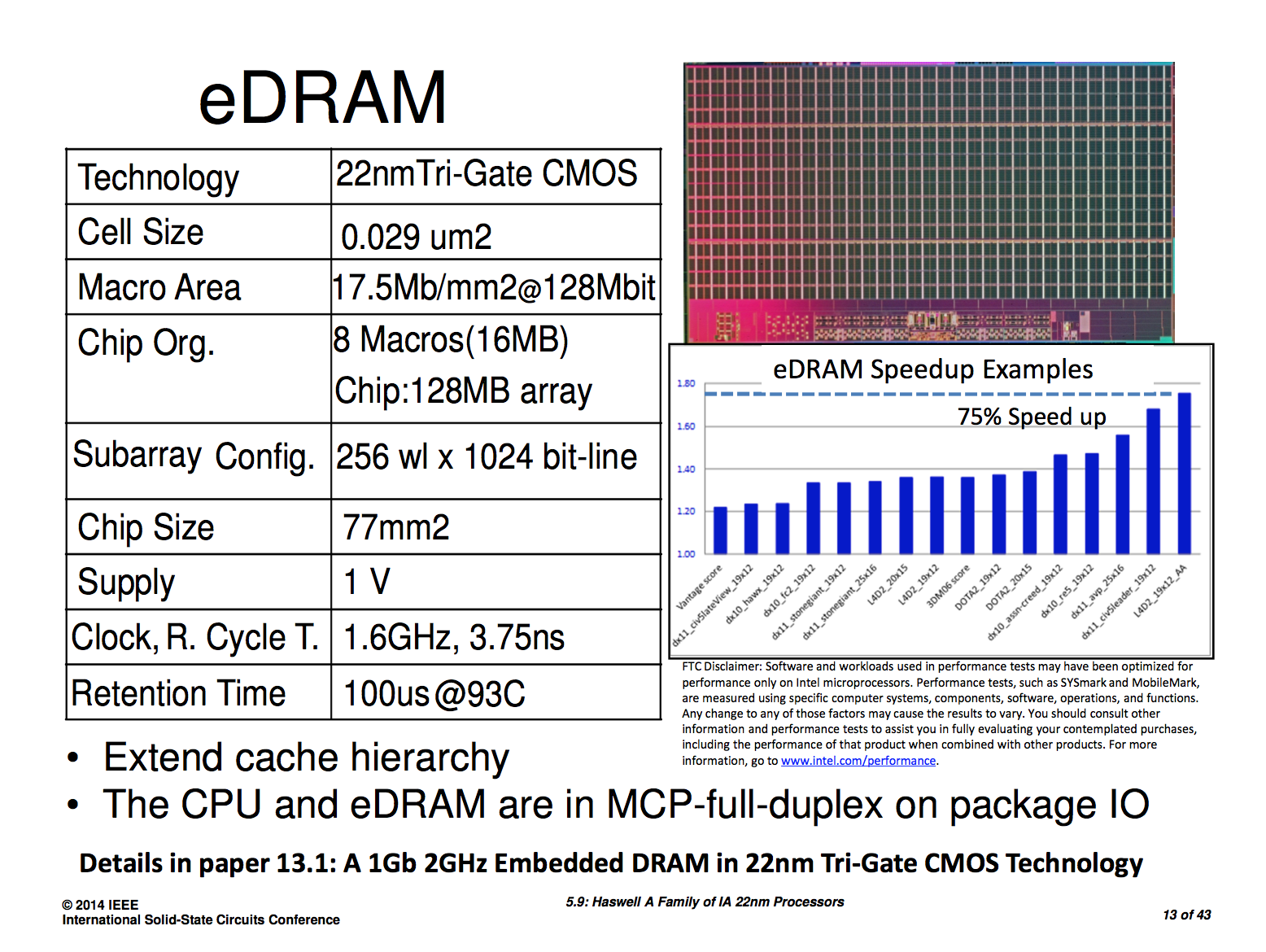
The 128MB eDRAM is divided among eight 16MB macros. The eDRAM operates at 1.6GHz and connects to the outside world via a 4 x 16-bit wide on-package IO (OPIO) interface capable of up to 6.4GT/s. The OPIO is highly scalable and very area/power efficient. The Haswell ULT variants use Intel's on-package IO to connect the CPU/GPU island to an on-package PCH. In this configuration the OPIO delivers 4GB/s of bandwidth at 1pJ/bit. When used as an interface to Crystalwell, the interface delivers up to 102GB/s at 1.22pJ/bit. That amounts to a little under 1.07W of power consumed to transmit/receive data at 102GB/s.
By keeping the eDRAM (or PCH) very close to the CPU island (1.5mm), Intel can make the OPIO extremely simple.
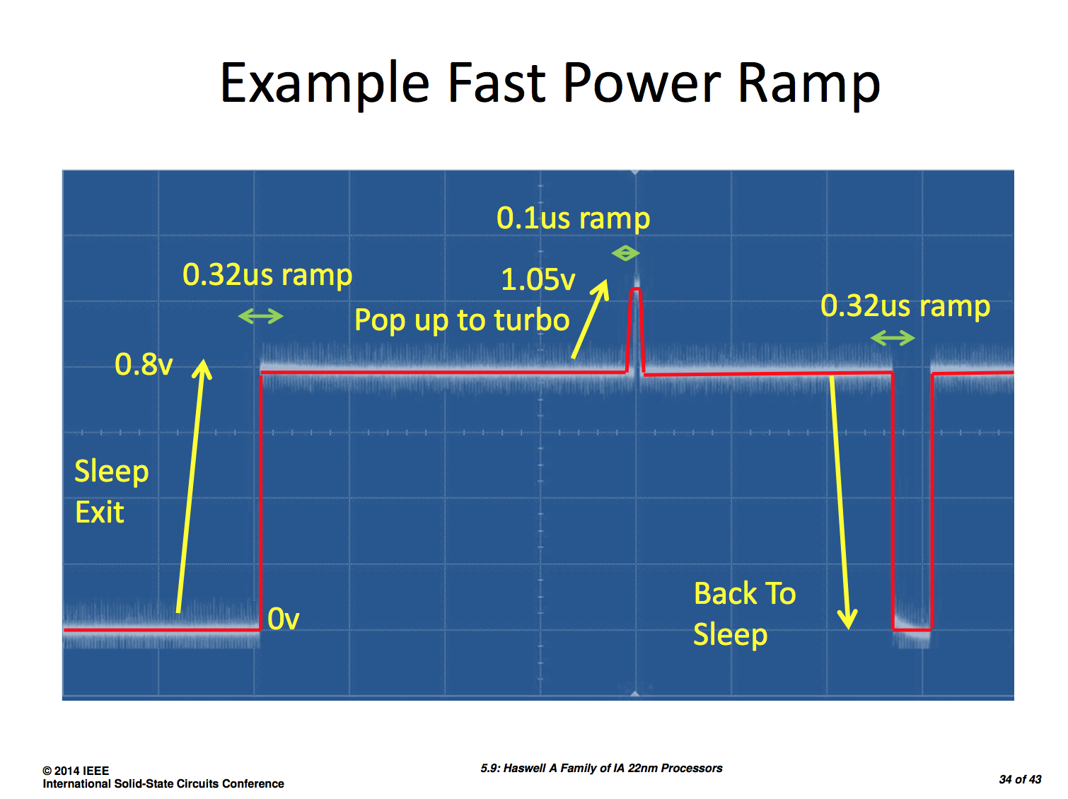
Intel also shared some data on how it achieved substantial power savings with Haswell, including using a new stacked power gate for the memory interface that reduced leakage by 100x over Ivy Bridge. Haswell's FIVR (Full Integrated Voltage Regulator) is also a topic of discussion in Intel's ISSCC papers. FIVR ends up being 90% efficient under load and can enter/exit sleep in 0.32µs, requiring only 0.1µs to ramp up to turbo frequencies.
Intel's Haswell ISSCC disclosures don't really change anything about Haswell, but they do further illustrate just how impressive of a design it is.


44 Comments
View All Comments
Akaz1976 - Monday, February 10, 2014 - link
Does any of this mean that we can get a core i5 processor in an ipad like form factor (with 10+ battery life & full win8)?jimjamjamie - Monday, February 10, 2014 - link
Surface Pro 2?azazel1024 - Monday, February 10, 2014 - link
Well, Akaz, you can get a Bay Trail-T based processor in an iPad like format that gets 10+hrs of battery life and runs full Windows 8.1.Its not an i5, but is pretty nice.
Come Airmont/Cherry Trail-T this coming fall, and that should be a rather impressive thing too (though Bay Trail-T is actually pretty decent).
My T100 can easily push 10hrs of battery life in lightweight use and more than 12 just watching movies (about 5-6hrs in some pretty heavy gaming). Its still a bit of a lightweight compared to my i5 3317u based laptop, but it ain't shabby either. Not very noticable in basic tooling around the OS and web based stuff. Just noticable in things like photoshop and lightroom (and gaming), but even there, it can get the job done, so long as you aren't expecting full laptop/desktop levels of performance.
mikk - Tuesday, February 11, 2014 - link
~180mm² for 2+2 ULT is nonsense, this is as big as 4+2 Haswell. 130mm² is more accurate.