Inside the First Android Wear Devices: LG G Watch & Samsung Gear Live Teardown
by Anand Lal Shimpi on June 30, 2014 4:50 PM EST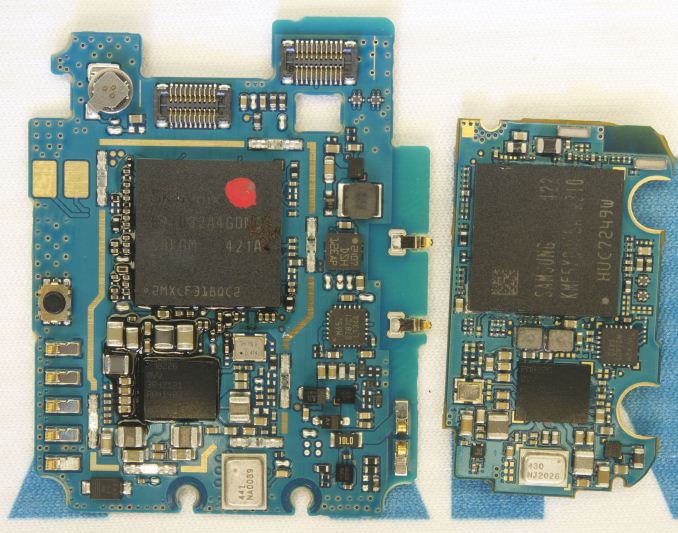
Last week at IO, Google gave attendees a choice of one of two Android Wear devices to take home and get experience with the platform. Although I personally opted for LG's G Watch (the display looked better), my friend James Bruce at ARM managed to get both and spent the next day taking them apart. James sent over high res pics of the result and gave us permission to post the images here (Update: ARM posted its own blog on the teardown here). I'm working on a review of Android Wear and the G Watch now (and yes, I have battery life data), but I hadn't yet taken it apart.
LG G Watch
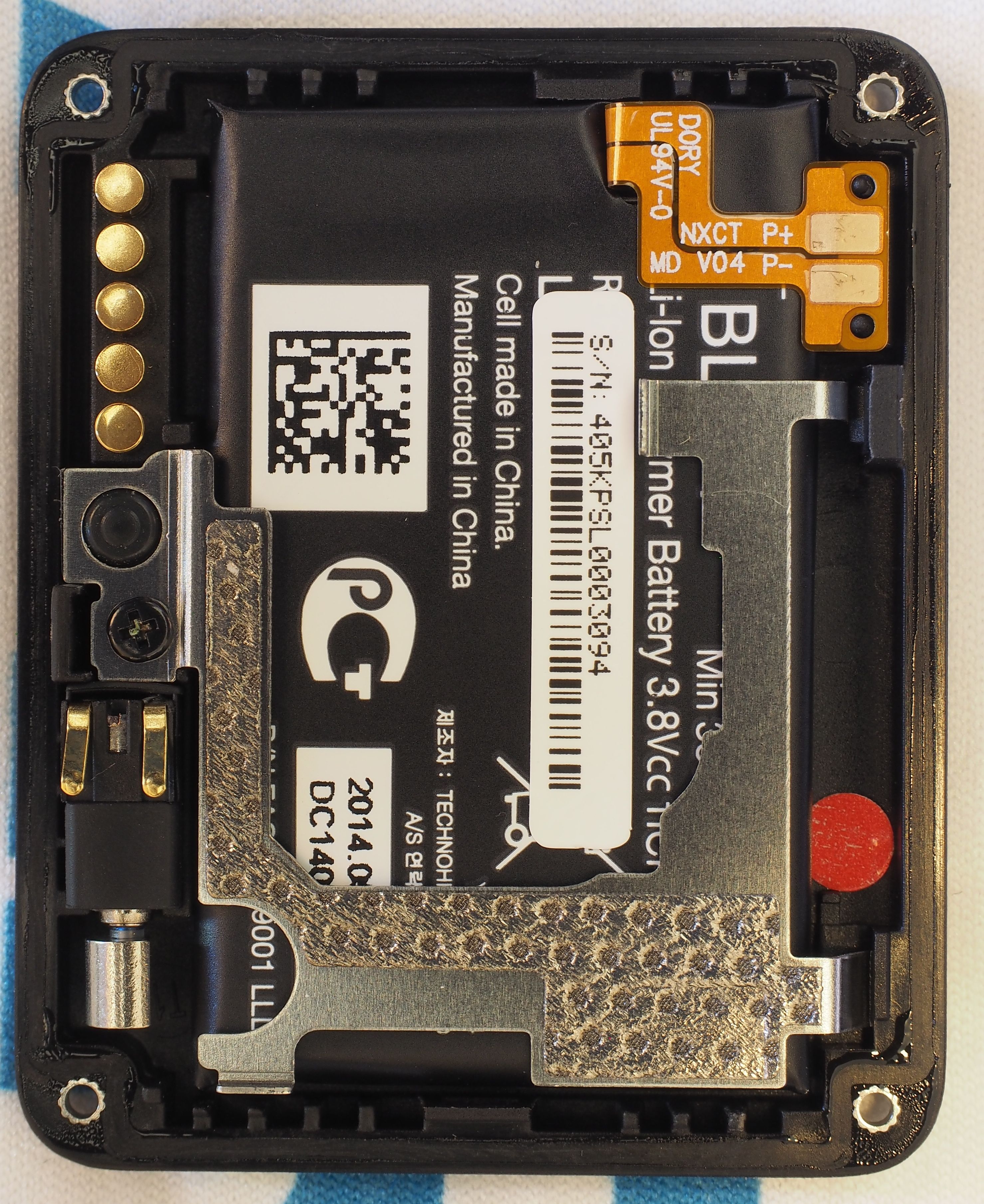
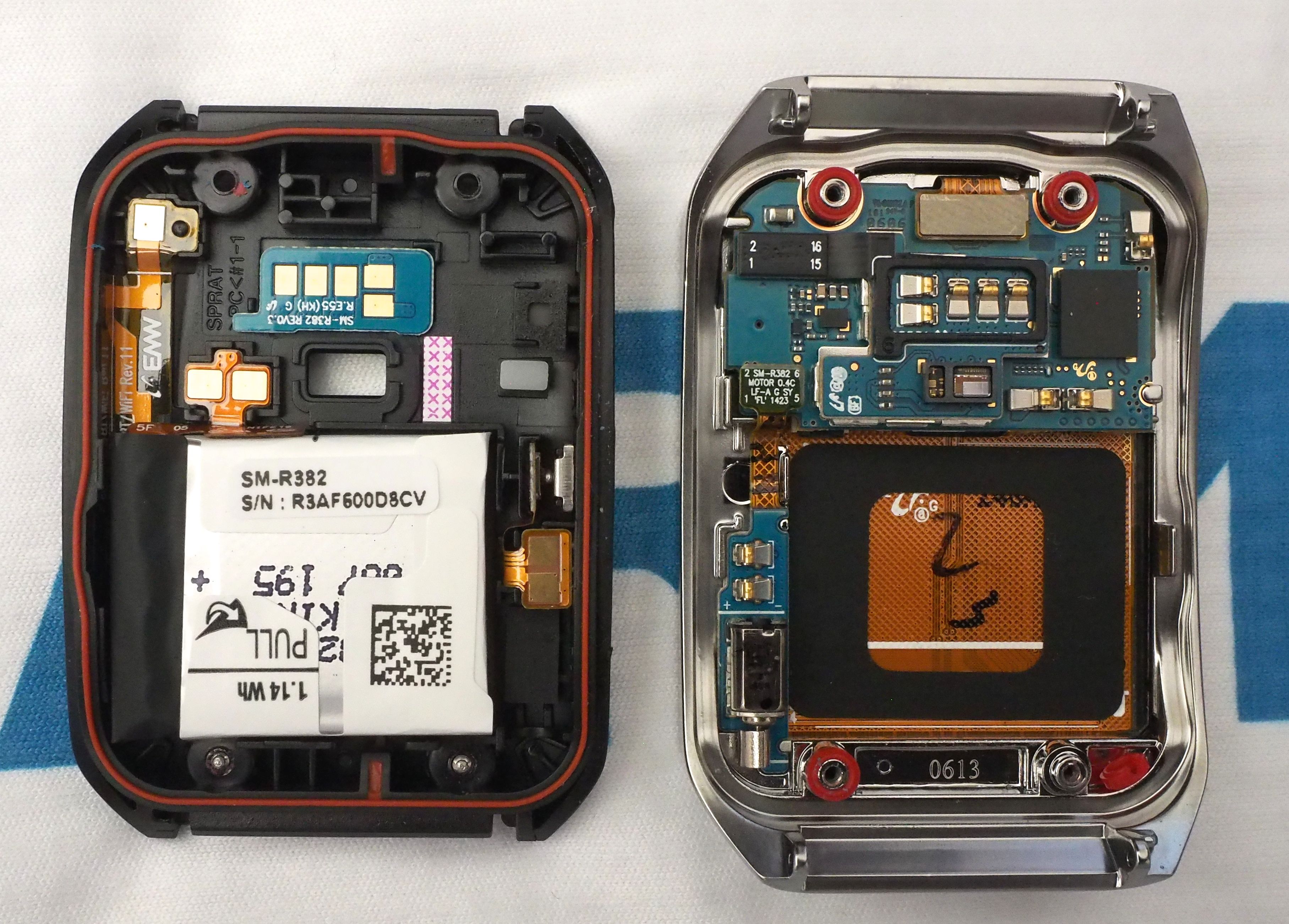
The G Watch turns out to be pretty easy to take apart. There are four Torx T5 screws on the back, removing them gives you access to its internals. The 400mAh battery is integrated into the back cover. ARM's teardown confirms 3.8V chemistry, resulting in a 1.52Wh total capacity.
 LG G Watch
In the photo above (left) you can see the thin gasket that runs around the perimeter of the G Watch, helping to give it its IP67 rating (fully sealed against dust, submergible in up to 1 meter of water for up to 30 minutes).
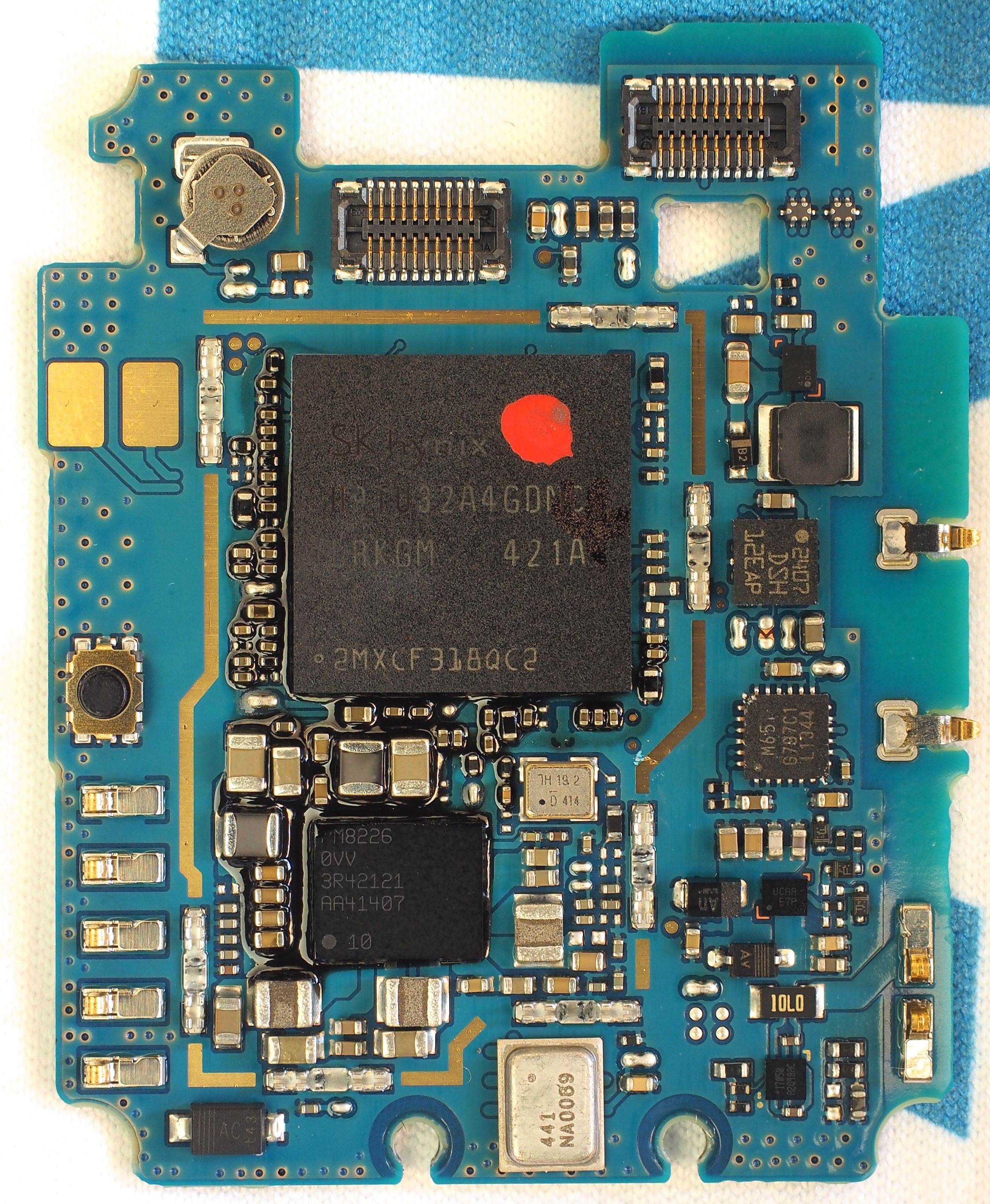
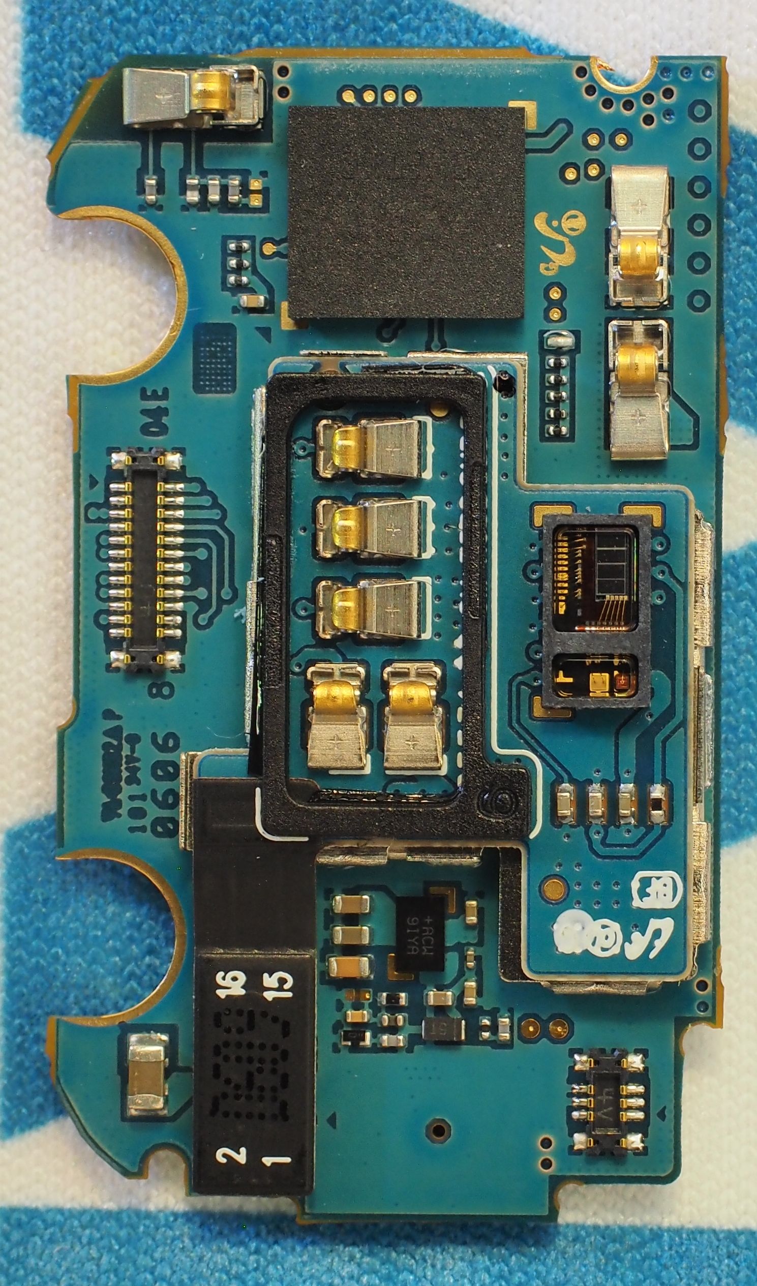
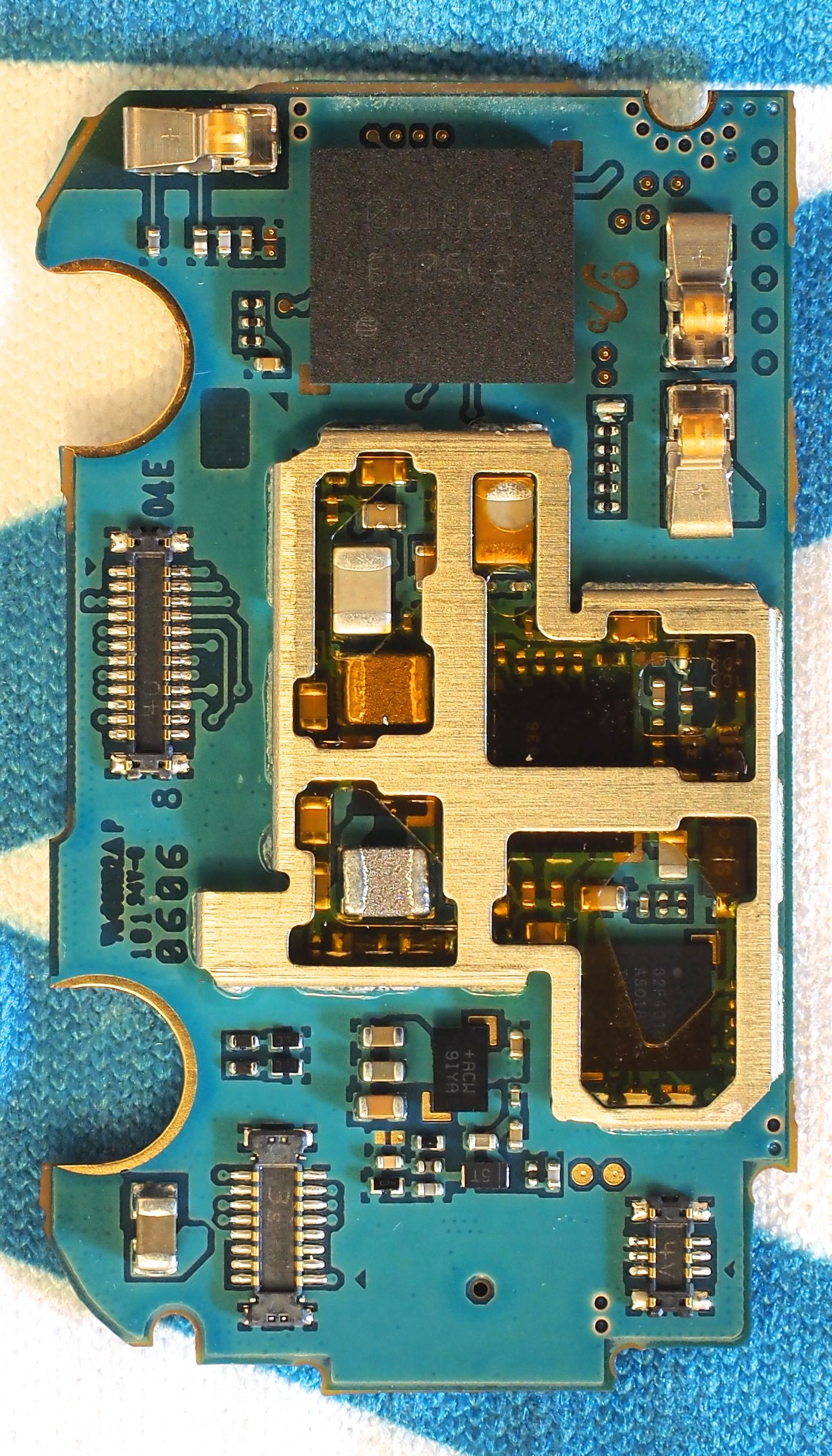
Two more screws hold the incredibly small PCB in place. The Qualcomm APQ8026 SoC (4 x Cortex A7 + Adreno 305 graphics) is underneath the Hynix DRAM device. There's a discrete Qualcomm PM8226 PMIC just south of the SoC.
 LG G Watch
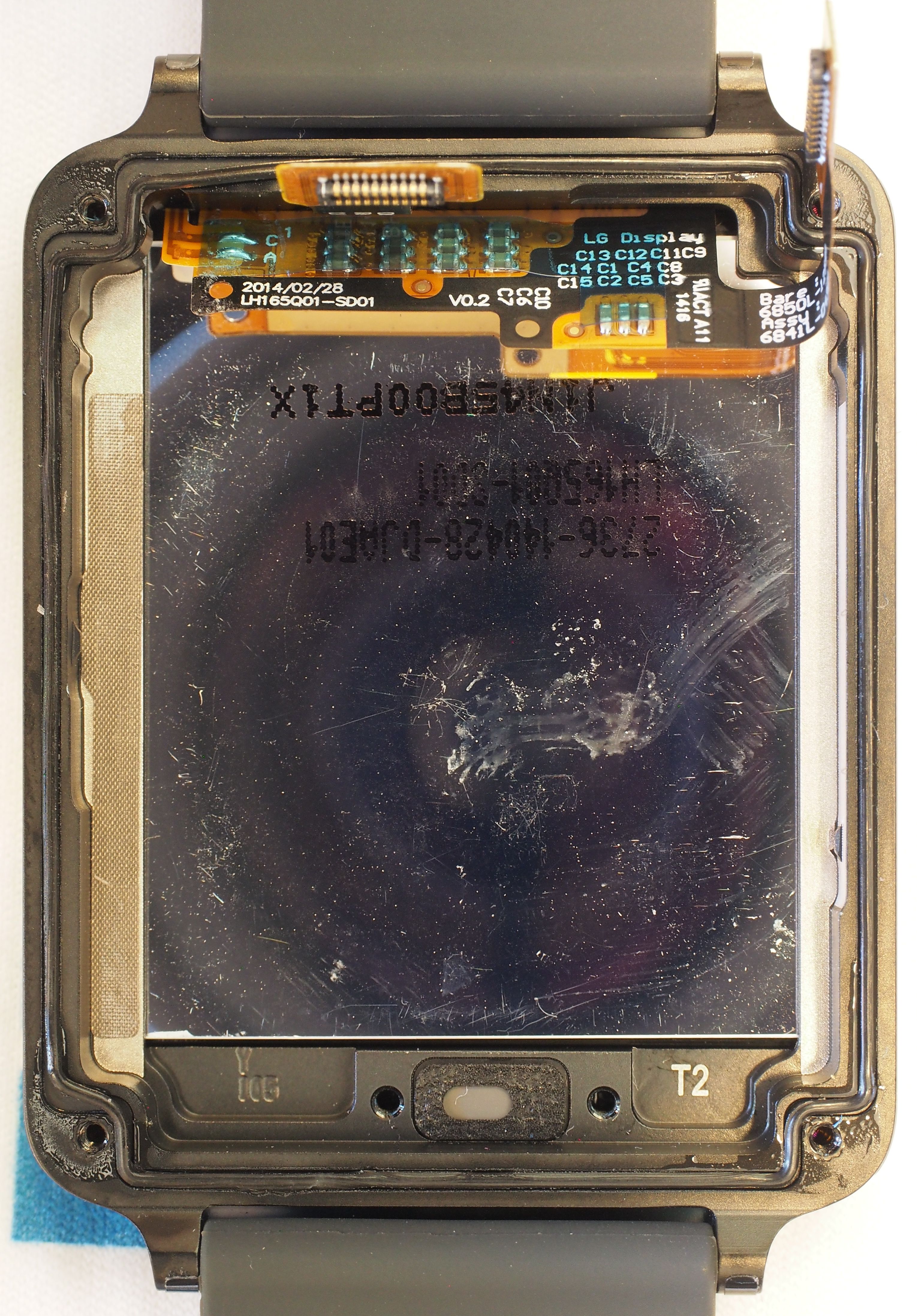
On the flip side of the PCB we see Synaptics' touch controller (the same model used in the Moto X).


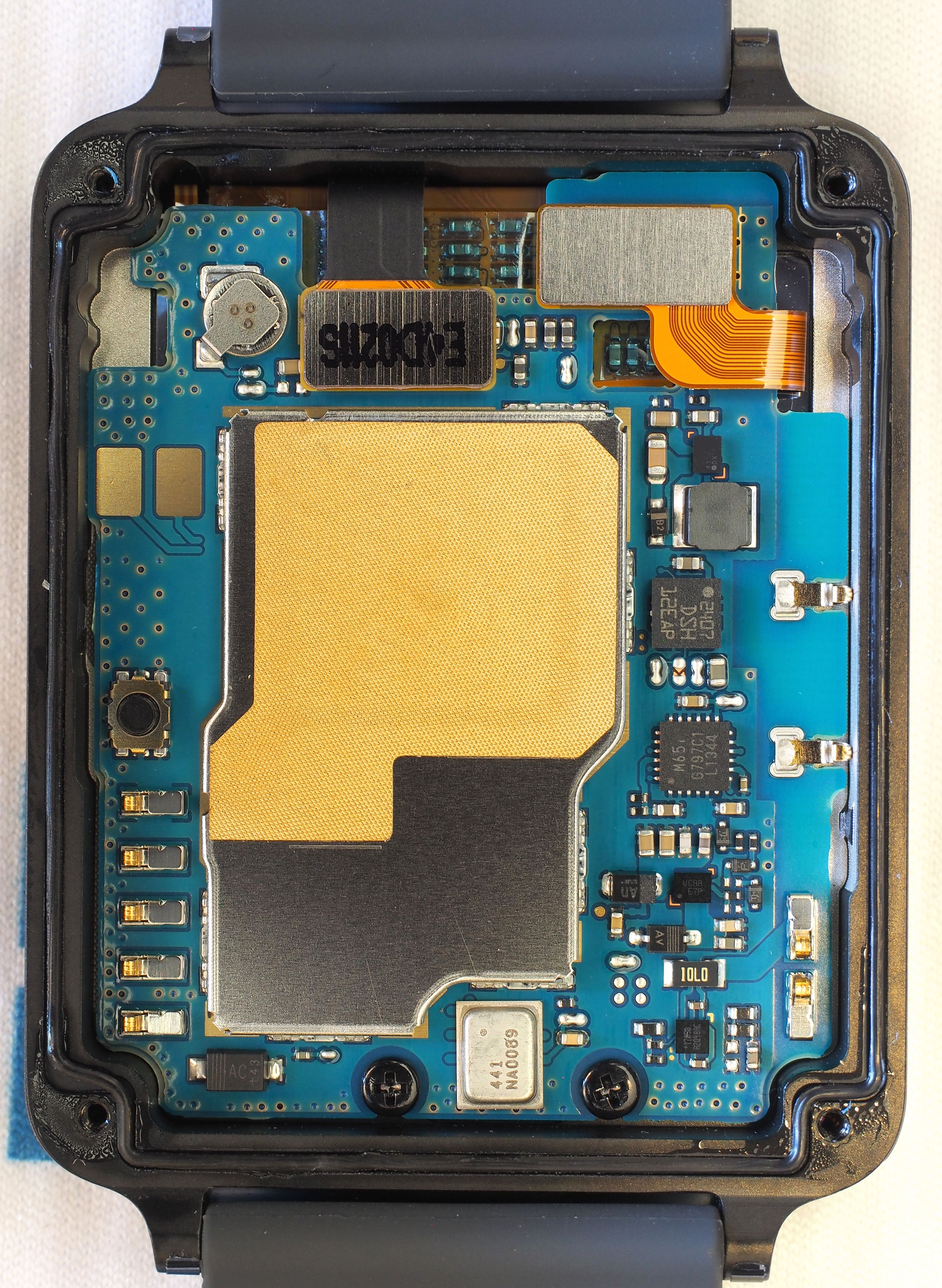
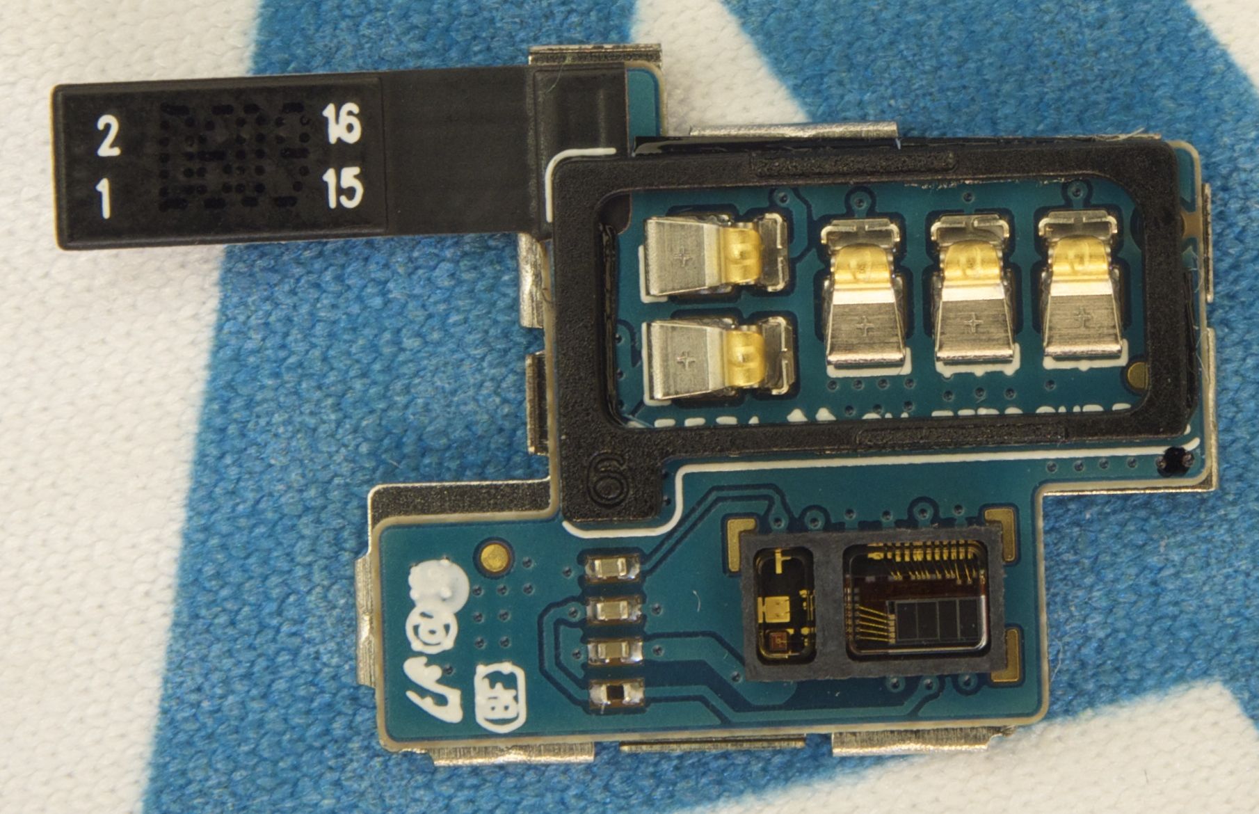
The Gear Live is also held together by four screws, although dismantling the watch takes a little more effort. The battery and heart rate monitor are both enclosed in the back of the watch. Samsung is also using 3.8V chemistry for its watch battery.
 Samsung Gear Live
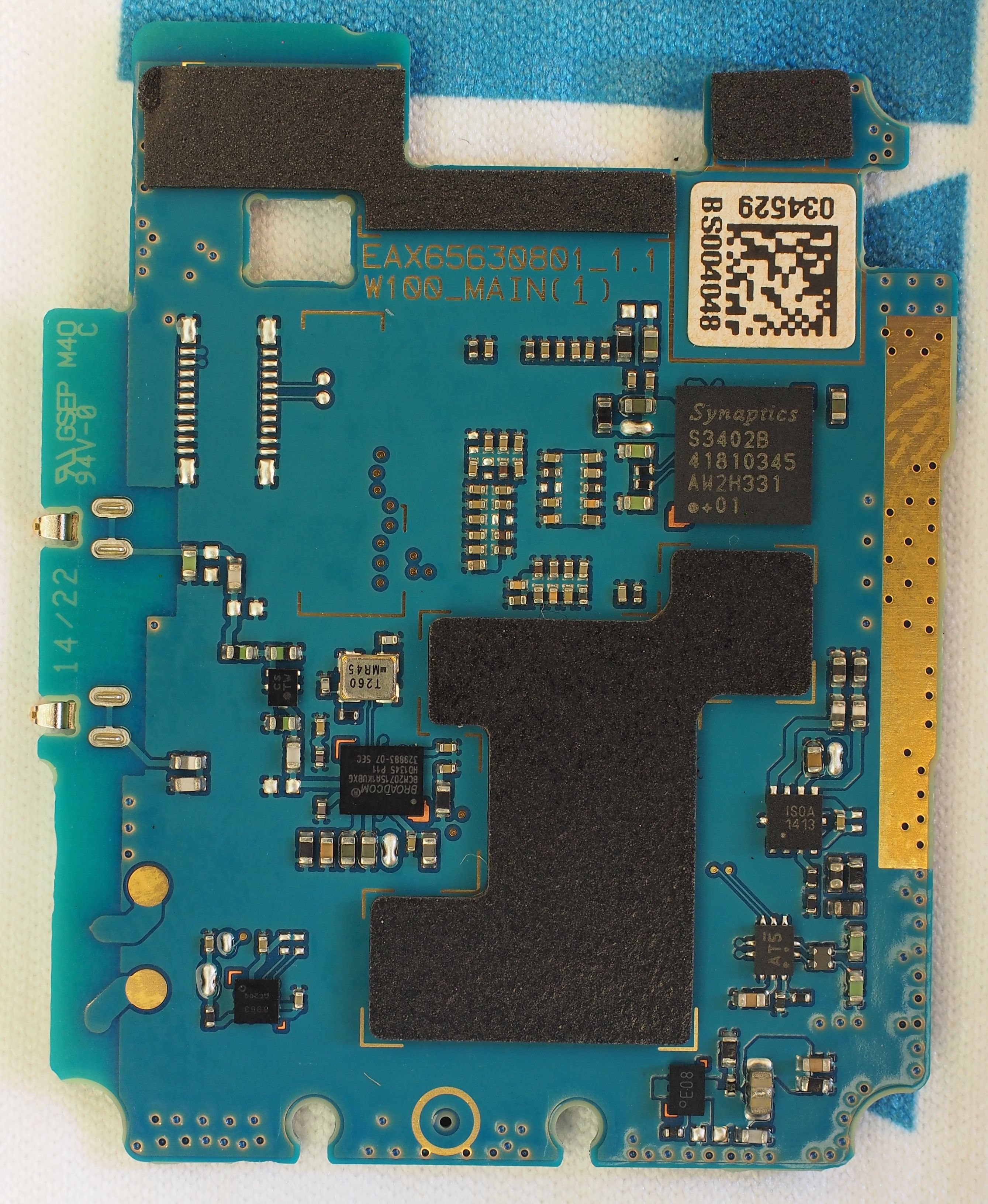
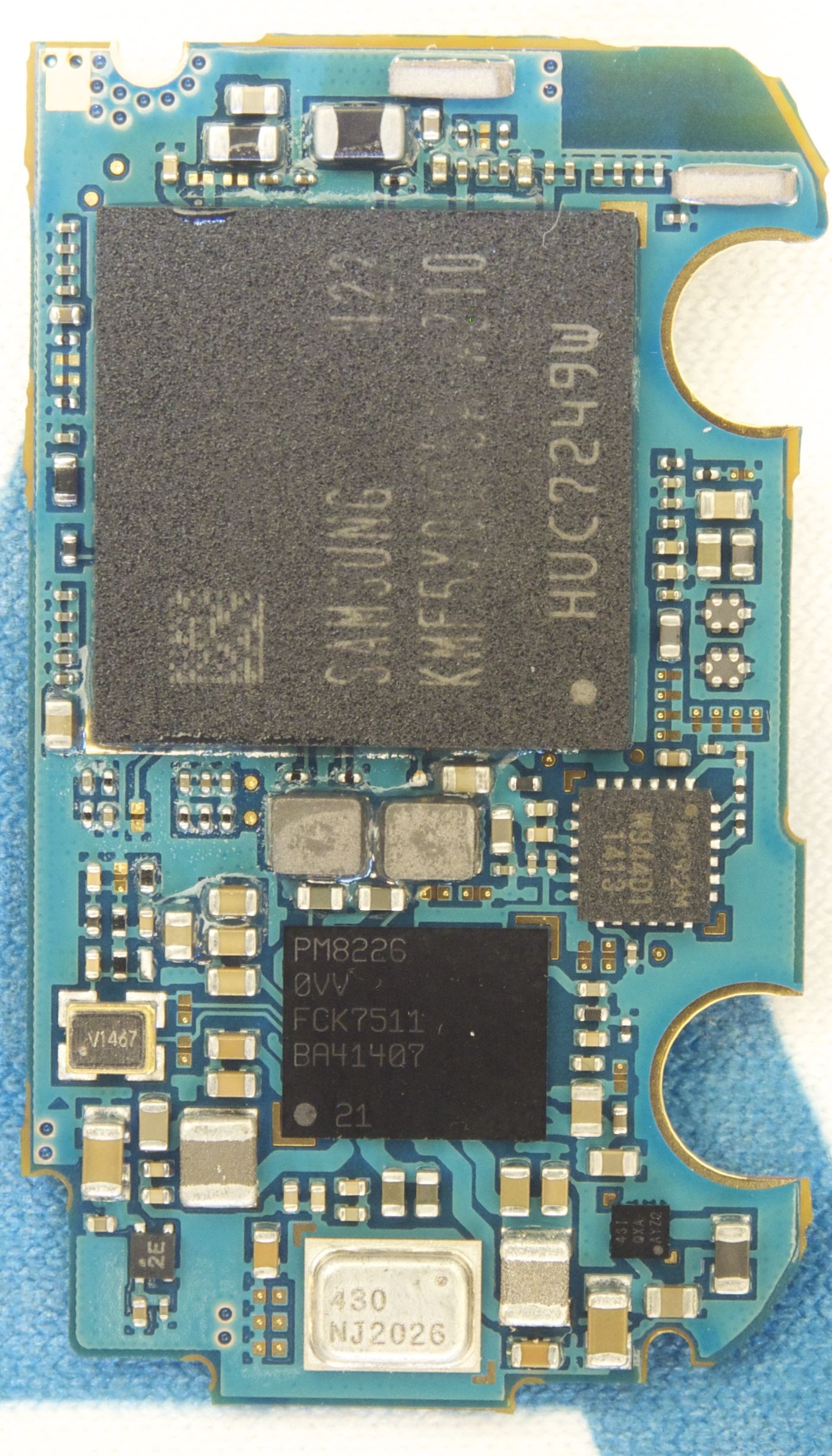
The logic board in the Gear Live is a bit more complex. There's a second layer stacked on the main logic board that also acts as an RF can.
Samsung Gear Live
We see the same APQ8026 SoC from Qualcomm below a Samsung DRAM device in a PoP stack.
Samsung Gear Live
Overall Samsung definitely has the more compact (and complex) internal PCB (the picture at the top of the article compares the two side by side), which makes sense given the company's relative head start in this space.


There's been a ton of innovation in the internal layout of smartphones over the years. As these are the very first Android Wear devices, it'll be interesting to see how the internal structure evolves over the coming years. One thing is for sure: those batteries are going to have to get thinner, or find a new place to live. Perhaps split up and distributed into a watch band?


26 Comments
View All Comments
uhuznaa - Tuesday, July 1, 2014 - link
Yes, I thought the same. These things almost look like prototypes, there's a lot you could do with deeper integration here. Just shows that they aren't really committed to the very idea of smartwatches it seems. The quad-cores with only one core enabled also show that this is just about getting something out of the door as quickly as possible.I'm more and more curious about what Apple will come up with.
tuxfool - Tuesday, July 1, 2014 - link
Indeed. The Pebble Smartwatch has all of its internals on flexpcb.787b - Monday, June 30, 2014 - link
http://images.anandtech.com/doci/8228/Android%20We...Anyone knows what is the black tar on PCB next to RAM/SoC stack?
smkennedy - Monday, June 30, 2014 - link
It's a underfill material to help keep the BGA (ball grid array) packages from popping off the board if it is flexed. Essentially a glue to hold the chips on and improve reliability. Most smartphones will have it as well.787b - Tuesday, July 1, 2014 - link
Thanks. I guess Samsung uses less glue than LG, so it can't be seen on the picture.Devo2007 - Monday, June 30, 2014 - link
You mentioned the LG display looked better, but was the Samsung "bad?" In what way was the LG better?ahse0w - Monday, June 30, 2014 - link
I wonder if the watch gets hot under load.Or there is no such power intensive app for the smartwatches yet..
michaelljones - Monday, June 30, 2014 - link
Looks like sensor wins for Invensense in both cases as well. A M65x class part in the LG and a M92x class part in the Samsung.Gadgety - Tuesday, July 1, 2014 - link
Very interesting piece."One thing is for sure: those batteries are going to have to get thinner, or find a new place to live. Perhaps split up and distributed into a watch band?"
I saw somewhere a battery in the watch band has been patented by Apple. Looking forward to the patent battles, injuctions, bans, counter suing etc.
Gadgety - Tuesday, July 1, 2014 - link
On the LG G Watch "Two more screws hold the incredibly small PCB in place."then
"Overall Samsung definitely has the more compact (and complex) internal PCB (the picture at the top of the article compares the two side by side)"
If LG's PCB is incredibly small, what superlative could be used to describe Samsung's? Even incredibly smaller?
On a side note, I missed the battery capacity of the Samsung.
Looking forward to the review.