A Quick Look at the GS5 LTE-A Subpixel Layout
by Joshua Ho on August 29, 2014 4:47 PM EST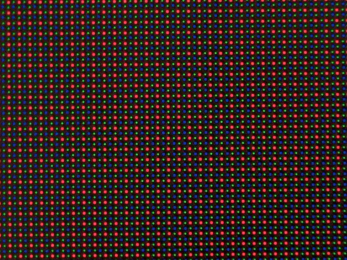
While it was easy to make an educated guess that the Galaxy S5 LTE-A Broadband had a PenTile subpixel layout to support the higher pixel density, I didn't get visual confirmation of this until now. While this picture is rather boring, it's much more interesting to see the display when turned off.
There are a few observations to be made from this photo. While it definitely looks disconcerting and creepy to some, it's possible to make out that there's something set in between the green subpixels when viewed diagonally. This appears to be where the transistors are placed to control a given subpixel. It also seems that the deposition process isn't perfect, as there's noticeable variance in shape and size among subpixels of a given color. This probably explains why the display isn't quite uniform when viewing it at near-black levels. It also appears that there may be an upper bound to how tightly Samsung can place two distinct emitter materials together, as this arrangement has noticeable levels of dead space in between subpixels. In order to better see the full picture, I've included a short gif of the display turning on and off.


21 Comments
View All Comments
jann5s - Monday, September 1, 2014 - link
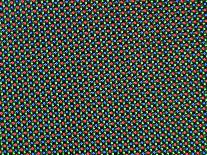
Ah, I understand my confusion, LCD's do not use a bayer pattern, but a stripe pattern.Quote from the wiki page about the Pentile_Matrix_Family: "Thus the RG-BG scheme creates a color display with one third fewer subpixels than a traditional RGB-RGB scheme but with the same measured luminance display resolution.[5][6] This is similar to the Bayer filter commonly used in digital cameras."