DDR4 Haswell-E Scaling Review: 2133 to 3200 with G.Skill, Corsair, ADATA and Crucial
by Ian Cutress on February 5, 2015 10:10 AM EST
For any user interested in performance, memory speed is an important part of the equation when it comes to building your next system. This can apply to any user, from integrated graphics throughput to gaming and prosumer environments such as finance or oil and gas. Individuals with an opinion on memory speed fall into two broad camps, from saying faster memory has no effect, to the ‘make sure you get at least XYZ’. Following on from our previous Haswell DDR3 scaling coverage, we have now secured enough memory kits to perform a thorough test of the effect of memory speed on DDR4 and Haswell-E.
DDR4 vs. DDR3
On the face of it, direct comparisons between DDR4 and DDR3 are difficult to make. With the switch over from DDR2 to DDR3, there were some platforms that could use both types of memory and we could perform tests on both in the same environment. The current situation with DDR4 limits users to the extreme platform only, where DDR3 is not welcome (except for a few high minimum-order-quantity SKUs which are rarer than hens teeth). The platform dictates the memory compatibility, and the main characteristics of DDR4 are straightforward.
DDR4 brings to the table a lower operating voltage, down from 1.5 volts to 1.2 volts. This is the main characteristic touted by the memory manufacturers and those that use DDR4. It does not sound like a lot, especially when we can be dealing with systems from 300W to 1200W quite easily under Haswell-E. The quoted numbers are a 1-2W saving per module per system, which for a fully laden home-user desktop might approach 15W at the high end of savings over DDR3, but for a server farm with 1000 CPUs, this means a 15kW saving which adds up. The low voltage specification for DDR4L comes down from DDR3L as well, from 1.35 volts to 1.05 volts.
| DRAM Comparison | |||
| Low Voltage |
Standard Voltage |
Performance Voltage |
|
| DDR | 1.80 V | 2.50 V | |
| DDR2 | 1.80 V | 1.90 V | |
| DDR3 | 1.35 V | 1.50 V | 1.65 V |
| DDR4 | 1.05 V | 1.20 V | 1.35 V |
The lower voltage is also enhanced by voltage reference ICs before each memory chip in order to ensure that a consistent voltage is applied across each of them individually rather than the whole module at once. With DDR3, a single voltage source was applied across the whole module which can cause a more significant voltage drop, affecting stability. With this new design any voltage drop is IC dependent and can be corrected.
The other main adjustment to make from DDR3 to DDR4 is the rated speed. DDR3 JEDEC specifications started at 800 MTs and moved through to 1600 MTs, while some of the latest Intel DDR3 processors moved up to 1866 and AMD up to 2133. DDR4’s initial JEDEC for most consumer and server platforms is set at 2133 MHz, coupled with an increase in latency, but is designed to ensure that persistent transfers are quicker but overall latency is comparable to that of DDR2 and DDR3. Technically there is a DDR4-1600 specification for scenarios that want the bargain basement memory and are unfazed by actual performance.
As a result of this increase in speed, overall bandwidth is increased as well.
| Bandwidth Comparison | |||||
| Bus Clock | Internal Rate | Prefetch | Transfer Rate | Channel Bandwidth | |
| DDR | 100-200 MHz | 100-200 MHz | 2n | 0.20-0.40 GT/s | 1.60-3.20 GBps |
| DDR2 | 200-533 MHz | 100-266 MHz | 4n | 0.40-1.06 GT/s | 3.20-8.50 GBps |
| DDR3 | 400-1066 MHz | 100-266 MHz | 8n | 0.80-2.13 GT/s | 6.40-17.0 GBps |
| DDR4 | 1066-2133 MHz | 100-266 MHz | 8n | 2.13-4.26 GT/s | 12.80-25.60 GBps |
Latency moves from DDR3-1600 at CL 11 to DDR4-2133 at CL 15, which was an expected jump as JEDEC tends to increase CL by 2 for a jump in frequency. While having a latency of 15 clocks might come across as worse, the fact that the clocks are at 2133 MTs ensures that the overall performance is still comparable. At DDR3-1600 and CL11, time to initiate a read is 13.75 nanoseconds, compared to 14.06 nanoseconds for DDR4-2133 at CL15, which is a 2% jump.
One of the things that will offset the increase in latency is that CL15 seems to be a common standard no matter what frequency the memory is. Currently on the market we are seeing modules range from DDR4-2133 CL15 up to DDR4-3200 CL15 or DDR4-3400 CL16, marking a read latency down to 9.375 nanoseconds. With DDR3, we saw kits of DDR3-2400 CL10 for 8.33 nanoseconds, showing how aggressive memory manufacturing over the lifetime of the product can increase the efficiency.
Another noticeable difference from DDR3 to DDR4 is the design of the module itself.
DDR3 (top) vs DDR4 (bottom)
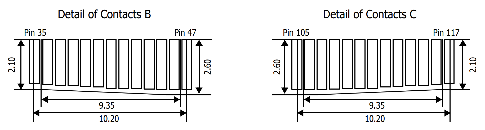
As with most technology updates notches are shifted in order to ensure that the right product fits in the right hole, but DDR4 changes a bit more than that. DDR4 is now a 288-pin package, moving up from 240-pin in DDR3. As the modules are the same length, this means a reduction in pin-to-pin distance from 1.00 mm to 0.85 mm (with a ±0.13 tolerance), decreasing the overall per-pin contact.
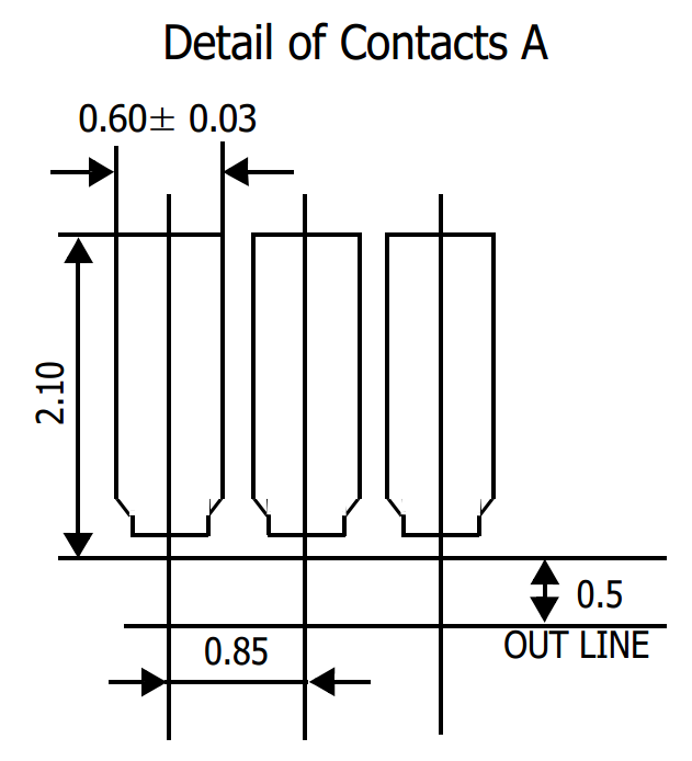
The other big design change is the sticky-out bits in the middle. Moving from pin 35 to pin 47, and back from pin 105 to pin 117, the pin contacts get longer as well as the PCB by 0.5 mm.

This is a gradient change rather than a full quick change:
Initially when dealing with these modules, I had the issue of not actually placing them in the slot correctly when using a motherboard with single sided latches. Over the past couple of weeks it has started to make more sense to place both ends in at the same time due to this protruding design, despite the fact it can be harder to do when on your hands and knees in a case.
Along with the pin size and arrangement, the modules are ever so slightly taller than DDR3 (31.25 mm rather than 30.35mm) to make routing easier, and the PCB is thicker (1.2 mm from 1.0 mm) to allow for more signal layers. This has implications for future designs, which we will mention later in the review.
There are other non-obvious benefits and considerations baked into the DDR4 design to mention.
DDR4 supports a low-power auto self-refresh (listed in the documentation as LPASR) which does the standard thing of refreshing the contents of memory but uses an adaptive algorithm based on temperature in order to avoid signal drift. The refreshing modes of each module will also adjust each array independently as the controller must support a fine-grained optimization routine to also coincide which parts of the memory are being used. This has power as well as stability implications for the long term future of DDR4 design.
Module training when the system boots is also a key feature of DDR4. During the start-up routine, the system must sweep through reference voltages to find a maximum passing window for the speeds selected rather than just apply the voltage in the options. The training will go through the voltage reference in steps from 0.5% of the VDDQ (typically 1.2V) to 0.8% and the set tolerance of the module must be within 1.625%. Calibration errors are plausible at one step size (9.6 mV at 1.2V) but also the slew margin loss due to calibration error must also be considered. This is due to the greater implication of losses due to margins and tolerances and ensures stable operation during use. The downside to the user is that the number of modules in the system effects the boot time of the device. A fully laden quad-channel Haswell-E system adds another 5-8 seconds to perform this procedure, and it is something that cannot be circumvented through a different routine without disregarding part of the specifications.
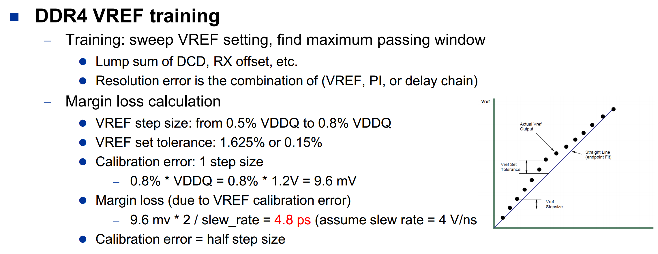
Source: Altera
DDR4 is also designed with the future in mind. Current memory on the market, except what we saw with Intelligent Memory, is a monolithic die solution. The base JEDEC specification will allow for 3D stacking of dies with through-silicon-vias (TSVs) should any memory manufacturer wish to go down this route to increase module density. To support this adjustment there are 3 chip select signals, bringing the total of bank select bits to 7 for a total of 128 possible banks. At current UDIMM specifications, there is provision for up to 8 stacked dies, however DDR4 is listed only to support x4/x8/x16 ICs with capacities of 2, 4, 8 and 16 Gibit (gibibit). This would suggest that the stacked die configuration is more suited to devices where x-y dimensions are a premium, or in the server markets. When it comes to higher capacity modules, we have already reported that 16GB UDIMMs should be coming to market, representing an 8*16Gb dual rank arrangement. We are working to make sure we can report on these as soon as they land, however when it comes to higher density UDIMM parts (i.e. not RDIMM or LRDIMM) we might have to start looking at newer technologies.
There are a significant number of other differences between DDR4 and DDR3, but most of these lie in the electronic engineer/design role for the memory and motherboard manufacturers, such as signal termination, extra programmable latencies and internal register adjustment. For a more in-depth read into these, a good Google search can yield results, although a thorough understanding of Rajinder Gill’s AnandTech piece about ‘Everything You Always Wanted To Know About SDRAM But Were Afraid To Ask’ is a great place to start about general memory operation. I still go back and refer to that piece more frequently than I admit, and end up scratching my head until I reach bone.


120 Comments
View All Comments
jabber - Friday, February 6, 2015 - link
Well I've added into my T5400 workstation USB3.0, eSATA, 7870 GPU, SSHD and SSD. I haven't added SATA III as its way too costly for a decent card, plus even though I can only push 260MBps from a SSD, with 0.1ms access times I really can't notice in real world. The main chunk of the machine only cost around £200 to put together.Striker579 - Friday, February 6, 2015 - link
omg those retro color mb's....good timesWardrop - Saturday, February 7, 2015 - link
Wow, how did you accidentally insert your motherboard model in the middle of the word "provide"? Quite an impressive typo, lolmsroadkill612 - Saturday, September 2, 2017 - link
To be the devils advocate, many say there are few downside for most using 8 lane gpu vs 16 lanes for gpu.if nvme an ssd means reducing to 8 lanes for gpu to free some lanes, I would be tempted.
FlushedBubblyJock - Sunday, February 15, 2015 - link
Core 2 is getting weak - right click and open ttask manager then see how often your quad is maxxed at 100% useage (you can minimize and check the green rectangle by the clock for percent used).That's how to check it - if it's hammered it's time to sell it and move up. You might be quite surprised what a large jump it is to Sandy Bridge.
blanarahul - Thursday, February 5, 2015 - link
TOTALLY OFF TOPIC but this is how Samsung's current SSD lineup should be:850: 120 GB, 250 GB TLC with TurboWrite
850 Pro: 128 GB, 256 GB MLC
850 EVO: 500/512 GB, 1000/1024 GB TLC w/o TurboWrite
Because:
a) 500 GB and 1000 GB 850 EVOs don't get any speed benefit from TurboWrite.
b) 512/1024 GB PRO has only 10 MB/s sequential read, 2K IOPS and 12/24 GB capacity advantage over 500/1000 GB EVO. Sequential write speed, advertised endurance, random write speed, features etc. are identical between them.
c) Remove TurboWrite from 850 EVO and you get a capacity boost because you are no longer running TLC NAND in SLC mode.
Cygni - Thursday, February 5, 2015 - link
Considering what little performance impact these memory standards have had lately, DDR2 is essentially just as useful and relevant as the latest stuff... with the added of advantage of the fact that you already own it.FlushedBubblyJock - Sunday, February 15, 2015 - link
If you screw around long enough on core 2 boards with slight and various cpu OC's with differing FSB's and result memory divisors and timings with mechanical drives present, you can sometimes produce and enormous performance increase and reduce boot times massively - the key seems to have been a differing sound in the speedy access of the mechanical hard drive - though it offten coincided with memory access time but not always.I assumed and still do assume it is an anomaly in the exchanges on the various buses where cpu, ram, harddrive, and the north and south bridges timings just happen to all jibe together - so no subsystem is delayed waiting for some other overlap to "re-access".
I've had it happen dozens of times on many differing systems but never could figure out any formula and it was always just luck goofing with cpu and memory speed in the bios.
I'm not certain if it works with ssd's on core 2's (socket 775 let's say) - though I assume it very well could but the hard drive access sound would no longer be a clue.
retrospooty - Thursday, February 5, 2015 - link
I love reviews like this... I will link it and keep it for every time some newb doof insists that high bandwidth RAM is important. We saw almost no improvement going from DDR400 cas2 to DDR3-1600 CAS10 now the same to DDR4 3000+ CAS freegin 80 LOLmenting - Thursday, February 5, 2015 - link
depends on usage. for applications that require high total bandwidth, new generations of memory will be better, but for applications that require short latency, there won't be much improvement due to physical restraints of light speed