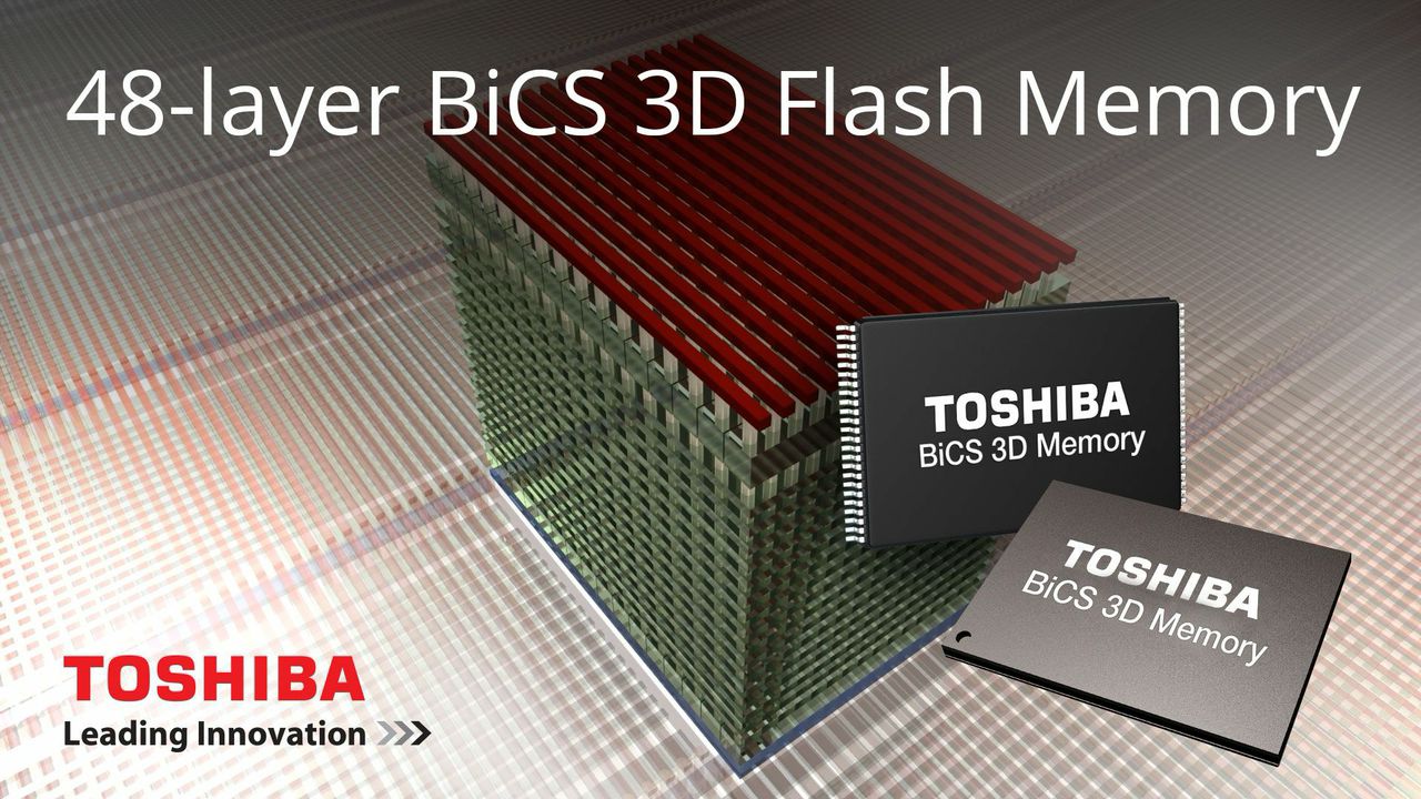
Toshiba Announces 48-layer 128Gbit 3D NAND - Samples Shipping Today
by Kristian Vättö on March 26, 2015 11:45 AM EST
The 3D NAND race is heating up. Samsung has been shipping its 3D NAND products for over six months now, but so far we have known very little about the others' 3D NAND technology. With today's announcement, Toshiba is shedding some light to its 3D NAND strategy by announcing that the company has started sampling a 48-layer 128Gbit (16GB) part.
Toshiba's 3D NAND structure (and also SanDisk's since the two have a NAND joint-venture) is called BiCS, which is abbreviation for Bit Cost Scaling. Similar to Samsung's TCAT structure, BiCS abandons the traditional floating gate design and utilizes a charge trap made out of insulating material to reduce electron leakage. From a structure and manufacturing standpoint, BiCS is quite different from TCAT, but given the amount of time and research required for a thorough analysis I'll save that for a later date. In the mean time, if you need a refresher on 3D NAND in general and Samsung's TCAT structure, I suggest you read our Samsung 850 Pro SSD review.
I'm not surprised that Toshiba's first 3D NAND product is a 48-layer part because the company has the smallest planar NAND node (15nm), so anything less than 48 would likely not have been cost efficient enough when compared against the 15nm node. There has been a lot of semiconductor analyst chatter about the optimal first generation high volume 3D NAND layer count and the consensus seems to be that you really need more than 32 layers to be competitive with modern planar NAND nodes because 3D NAND requires a whole new set of manufacturing tools that aren't exactly cheap. Toshiba did clarify that planar and 3D NAND will exist in parallel for some time, which suggests that even with 48 layers 3D NAND may be more expensive to manufacture than 15nm planar NAND (although that may change as the process matures and yields improve).
Initially Toshiba will be manufacturing 3D NAND in its Fab 5 at the company's Yokkaichi Operations in Japan, but the Fab 2 in the same location is expected to be up and running in the first half of 2016, which will increase Toshiba's 3D NAND output. While samples are shipping today, publicly available products are likely still at least a year away and I would expect the first products to arrive to the market in mid to late 2016. Given the late schedule, it's logical that Toshiba is going straight to 48 layers because Samsung will likely have a 48-layer design this year and I wouldn't be surprised to see Intel-Micron shipping one next year as well. Either way, next year is turning out to be very exciting in the NAND industry and it will be interesting to see whose 3D NAND process is the most advanced and cost efficient.
Source: Toshiba Press Release


13 Comments
View All Comments
jjj - Thursday, March 26, 2015 - link
Sandisk today cut their financial outlook and delayed their Investor Day so the timing for significant volume production might be in flux.If they are in trouble in enterprise and they are supply constrained overall ,they might try to launch this sooner.Khato - Thursday, March 26, 2015 - link
Haha, and what happens soon after this announcement by Toshiba? Intel/Micron announcing their entry into 3D NAND of course.Mark_gb - Thursday, March 26, 2015 - link
Thats hardly surprising. Samsung has been shipping 32 layer for half a year. Everyone else has been experimenting with their own variations of 3D NAND for over a year as well. Now they all want to get products out to customers ASAP, and so here come the announcements. Just watch though. At least some of these announcements will give and estimated delivery time frame, but expect those to slide backwards significantly as time goes by. Eventually though, all of these companies will release products using their variation of 3D technology.