The Samsung Exynos 7420 Deep Dive - Inside A Modern 14nm SoC
by Andrei Frumusanu on June 29, 2015 6:00 AM ESTThe Exynos 7420 - Inside a Modern SoC
At this point in time it’s undeniable that the Exynos 7420 seems to have a clear process advantage over the current competition, but before we go into more benchmarks and detailed power numbers, I’d like to take the opportunity to try to do something we haven’t done before: A dissection of what is actually inside of a modern SoC such as the Exynos 7420.
Over the past few years SoCs have grown more complex and transistor counts have shot up, but we rarely had the occasion to look into what kind of blocks are actually included in such large designs. PR material provided by companies often just include rough simplifications such as CPU core counts or GPU configurations. Some companies such as Qualcomm are even hesitant to give any kind of information on their IP – the Adreno GPU for example remains a mysterious black box when it comes to its architecture. Samsung SoC’s primary processing blocks are relatively well known because they use IP designed by ARM, with whom we have the opportunity and pleasure to extensively cover in articles such as our architectural deep-dives on the Mali Midgard design or ARM’s A53/A57 CPUs. While we feel we have a good understanding of the CPU and GPU, we know little of the remaining SoC components as they never get talked about.
Unfortunately when asking Samsung SLSI about details of the Exynos SoCs, LSI could not publicly comment on the architecture or details of current products. In order to try and learn more about this subject, I tried to reverse-engineer myself through the various IP blocks to re-create a high-level abstracted overview of what the SoC looks like.
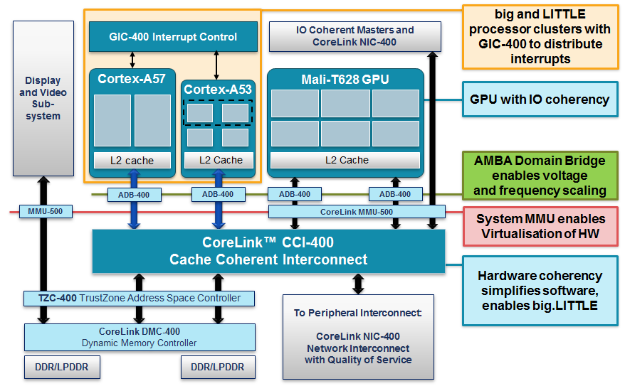
![]()
Before going into talking about the different blocks and layout, I’d like put a disclaimer out there that this graphic is purely an abstracted plan of the true physical layout. I did have access to a die shot of the chipset to base my analysis on, but we are unable to post this die shot. Blocks such as the GPU, CPUs and memory controllers can be considered to be representative of their actual size and location, other blocks such as the ISP and the top right quadrant are large functional simplifications for the purpose of presentation.
As mentioned in the manufacturing process section, the Exynos 7420 remains a relatively small SoC as it comes in at only 78mm². The biggest IP block is by far the Mali T760 GPU cluster sized at 17.7mm², consuming 22.6% of the SoC, nearly a quarter of the whole die. Historically speaking, this falls in line with what Samsung has previously budgeted for the GPU since the Exynos 5420. The individual shader cores are among one of the largest individual blocks on the SoC as they come in at 1.75mm². All 8 cores are connected via a common fabric and two islands of L2 cache. Samsung has officially disclosed the Exynos 5433’s Mali GPU to come with 512KB of total L2 cache – and size comparisons between the cache islands and shader cores of the two SoCs point out that the Exynos 7420 has a quite larger L2 to shader core ratio, pointing out to the possibility that its size may have doubled up to 512KB per MMU for a total of 1MB. We unfortunately won't know for sure until Samsung eventually releases more information on the Exynos 7420.
Moving on to other IP blocks we have concrete information on, we see the Cortex A57 “big” CPU cluster positioned in one corner of the SoC, largely opposite of the GPU. Again falling back to information released during ISSCC 2015, Samsung explains that this positioning is done for the best thermal management of the SoC. Having the two most power-consuming blocks as far from each other makes sense to try to keep hot-spots to a minimum and maximizing the thermal dissipation potential of the whole SoC.
The Cortex A53 “little” cluster is located right next to the A57 cluster. We see the same configuration as on the 5433 – four A53 cores with 256KB of L2 cache. The 14nm die shrink made it possible to make this the currently smallest modern 4-core cluster among existing SoCs as it comes in at only 2.71mm².
Between the two CPU clusters we find the ARM Cache Coherent Interconnect (CCI-400) that is the core IP that allows heterogeneous multiprocessing between different CPU architectures and is the corner-stone of big.LITTLE SoCs. Besides the CPU clusters, the CCI-400 can also connect three further slave IP blocks to form a group of cache coherent devices. This is the point where things get interesting; there is a general lack of public information from semiconductor vendors on how the CCI and general internal bus architecture looks like. For the Exynos 7420 I was able to confirm at least four of the five possible ports on the CCI.
Again, we have the obvious two CPU clusters each occupying a port on the CCI which is required for heterogeneous and simultaneous operation system of the two clusters. As further CCI slave devices, Samsung chooses to connect the G2D block (On the same port as the GPU) whose full name goes by FIMG2D (Fully Integrated Mobile Graphics 2D), which is the 2D graphics accelerator of Exynos SoCs. The G2D block is part of a larger block dedicated to 2D image manipulation called the MSCL – which is an acronym for M-Scaler although I’m not too sure what the M stands for, maybe Media? The overall block contains two dedicated hardware fixed-function image scalers as well as a JPEG compression and decompression unit. For example video streams will pass through this block to be re-scaled to a display’s resolution.
Another CCI-connected block is a new kind of IP that we haven’t seen before in the mobile space: a memory compressor. Blandly named “Exynos Memory Compressor” or M-Comp this is an interesting specialized piece of IP that has yet to play a role in the Galaxy S6. I’m quite certain this is a hardware block targeted and designed especially for Android. Since Android 4.4 kernel DRAM compression mechanisms have been a validated part of the OS and all devices come with a form or another of the feature. Most vendor devices come with the “zram” mechanism, which is a ramdisk with compression support. The kernel sets this up as a swapping device to store rarely used memory pages. Samsung had implemented this in its Galaxy devices as far back as Android 4.1.
The Galaxy S6 makes use of a more advanced implementation called “zswap” which is able to compress memory pages before they need to get swapped out to a swap device, so it’s a more optimized mechanism that sits closer to the kernel’s memory management core. An everyday example of its effects can be seen when multi-tasking a few apps: a sample readout shows it's able to compress 1.21GB of pages into 341MB of physical memory. Being able to offload the compression to a dedicated hardware block would be a great power efficiency optimization, so we’re hopefully looking forward to a future release and OS update of the device with a software stack that can use the hardware unit.
The memory compressor should be part of a larger block called “IMEM” which contains other elements such as the SSS (Security Sub-System). This is a hardware cryptographic accelerator that has been part of Exynos SoCs since the S5PC110 (Later renamed Exynos 3110) and is able to accelerate encryption and decryption for various ciphers. This includes a DMA engine so that it could directly have disk access for fast full disk encryption. I wasn’t able to confirm if the 7420 physically still has this block as it lacked any drivers. It may be possible Samsung has dropped it in favor of using the cryptographic capabilities of ARMv8, but it would still make sense to maintain a fixed-function IP block for power efficiency.
CCI-400 example layout as published by ARM and used in LG's Odin/Nuclun SoC
Exynos line of SoCs do not follow this arrangement.
As mentioned earlier, the one of the CCI ports is shared between the G2D block and the GPU. This is also a large difference to how ARM advertises its example SoC configuration of the CCI: we mostly see Mali GPUs get two ports on the CCI. This makes sense as each port is 128 bit wide in both read and write directions. Vendors have up until now been clocking the CCI at around half the DRAM frequency as most LPDDR3 SoCs saw it running at 400-466MHz. One example SoC which closely follows ARM’s depiction of such a bus architecture is LG’s Odin (Nuclun), as it runs two ports to the CCI running at 400MHz with 800MHz memory controllers. Having a single 128 bit port to the GPU will limit its bandwidth to only half the achievable bandwidth of 2x32bit memory controllers, so that’d be a waste of resources. Furthermore, the Exynos 7420 clocks the CCI at up to only 532MHz. This is an interesting divergence from the DRAM frequency / 2 rule we’ve seen until now, and also means that a single CPU cluster is technically unable to saturate main memory bandwidth on the 7420. The per-port bandwidth is limited to 8.5GB/s in read and write directions for a concurrent total of 17GB/s, a figure we’ll be able to correctly verify later on in the CPU performance section.
The last CCI port which I didn’t actually depict in the layout should go to the CoreSight block, ARM’s system IP for debugging and trace of SoCs.
This leaves the question open on how the GPU is actually connected to the memory controllers. One thing for sure, is that it doesn’t go through the CCI. Samsung calls their internal bus architecture a “Multi-Layer AXI/AHB Bus Architecture”. AXI and AHB are both specifications defined in ARM AMBA (Advanced Microcontroller Bus Architecture), an interconnect standard used in one way or another basically all of today’s SoCs. We know that there is at least a large 2-layer separation: An “Internal” bus which I depict in the SoC schematic as BUS0, a “Memory Interface” bus depicted as BUS1. There is also a less important peripheral bus that I left out due to it connecting smaller low-bandwidth IPs that are not as interesting to the discussion.
The memory interface bus operates on the same clock plane as the actual LPDDR4 memory controllers, reaching up to 1555MHz. The memory controllers physically are spread along two sides of the SoC die. Each memory controller has 2x 16bit interfaces directly to the DRAM dies. This means that the DRAM PoP module contains 4 DRAM dies, standard among 64-bit total bus width SoCs. The most trouble I’ve had in deciphering how the internal bus layout works was trying to understanding how the memory controllers interact with the various buses. It’s clear that Samsung’s bus architecture is quite more complex to the more simplistic designs we have public information about. Sadly, unless there will be future new resources we can fall upon on, the best we can do is to just have a guess on how main traffic flows throughout the chip.
Part of the internal bus blocks are all major I/O IP blocks. These are physically separated into two major blocks called FSYS0 and FSYS1. This includes 3 Synopsis DesignWare MMC controllers (2x 8bit, 1x 4bit) that can be used for eMMC, WiFi SDIO and external SD card connections. A MIPI UniPro controller for UFS 2.0 is of course also part of the interfaces for storage and is used for the NAND storage on the Galaxy S6.
Over the last year we’ve seen WiFi connectivity make a migration from SDIO interconnects to PCIe-based ones. Both Qualcomm and Samsung also did this migration for their top-end SoCs as they included PCIe controllers. The Galaxy Note 4 was one of the first phones to make this switch with Broadcom’s BCM4358 WiFi SoC. According to Broadcom, the reasons for this are two-fold. The first is for performance, as PCIe has significantly reduced processing overhead and DMA capability. The second is power efficiency, as the PCIe spec allows for lower and more fine-grained low power states than the SDIO interface.


114 Comments
View All Comments
jjj - Monday, June 29, 2015 - link
The power doesn't look that great, for the A57 seems to allow 300-350Mhz higher clocks, granted it's not a clean shrink. It looks good here because on 20nm they pushed the clocks way high.name99 - Monday, June 29, 2015 - link
Insofar as rumors can be believed, the bulk of A9's are scheduled to be produced by Samsung, presumably on this process. It seems strange to have Apple design/layout everything twice for the same CPU, so if these same rumors (30% going to TSMC) are correct, presumably that means the A9X will be on TSMC.As for characterizing Apple CPUs, while there are limits to what one can learn (eg in the voltage/power tradeoffs), there is a LOT which can be done but which, to my disappointment, has still not been done. In particular if someone wanted, I think there's scope for learning an awful lot from carefully crafted micro benchmarks. Agner Fog has give a large number of examples of how to do this in the x86 space, while Henry Wong at stuffedcow.net has done the same for a few less obvious parts of the x86 architecture and for GPUs.
It strikes me as bizarre how little we know about Apple CPUs even after two years.
The basic numbers (logical registers, window, ROB size) seem to about match Intel these days, and the architecture seems to be 6-wide with two functional clusters. There appears to be a loop buffer (but how large?) But that's about it.
How well does the branch prediction work and where does it fail?
What prefetchers are provided? (at I1, D1, L2. L3)
Do the caches do anything smart (like dead block prediction) for either performance or power?
Does the memory manager do anything smart (like virtual write queue in the L3)?
etc etc etc
Obviously Apple doesn't tell us these. (Nowadays the ONLY company that does is IBM, and only in pay-walled articles in their JRD.) But people write the micro benchmarks to figure this out for Intel and AMD, and I wish the same sort of enthusiasm and community existed in the ARM world.
SunnyNW - Wednesday, July 1, 2015 - link
Believe word on the street is the A9 will be Sammy 14nm and the A9X TSM 16nm+SunnyNW - Wednesday, July 1, 2015 - link
Please ignore this comment, should have read the rest of the comments before posting since Name99 already alluded to this below. SorryCiccioB - Monday, June 29, 2015 - link
Is the heterogeneous processing that allows all 8 cores working together active?Seen the numbers of the various bench it seems this feature is not used.
What I would like to know exactly is that is the bench number of this SoC can be directly compared to SoC with only 4 cores like the incoming Qualcomm Snapdragon 820 based on custom architecture which has "only" 4 cores and not a big.LITTLE configuration.
Andrei Frumusanu - Monday, June 29, 2015 - link
HMP is active. Why do you think it seems to be not used?CiccioB - Monday, June 29, 2015 - link
Because with 8 cores active (or what they should be with HMP) results is not even near 4x the score of a single core.So I wonder if those 8 core are really active. And whether they are of any real use if, to keep consumption adequate, frequencies of higher cores get limited.
Andrei Frumusanu - Monday, June 29, 2015 - link
All the cores are always active and they do not get limited other than in thermal stress situations. I didn't publish any benchmarks comparing single vs multi-core performance so your assumption must be based on something else. Having X-times the cores doesn't mean you'll have X-times the performance, it completely depends on the application.It's still a perfectly valid comparison to look at traditional quad-cores vs bL octa-cores. In the end you're looking at total power and total performance and for use-cases such as PCMark the number of cores used shouldn't be of interest to the user.
Refuge - Monday, June 29, 2015 - link
I would hazard a guess that thermal throttling has something to do with part of it.ruturaj1989@gmail.com - Monday, June 29, 2015 - link
It does have 4 cores but I guess they are in big.LITTLE configuration too. We will see shortly. HMP is active but I am not sure if every bench app uses all the cores.