Skylake CPU Package: Mini-Analysis
by Ian Cutress on August 10, 2015 6:00 AM EST
As a short side piece from our in depth review on Intel's 6th Generation Core processors, codename Skylake, the well-known overclocker Splave has posted some very interesting images on the processor itself. We confirmed we are free to use the pictures below from him.
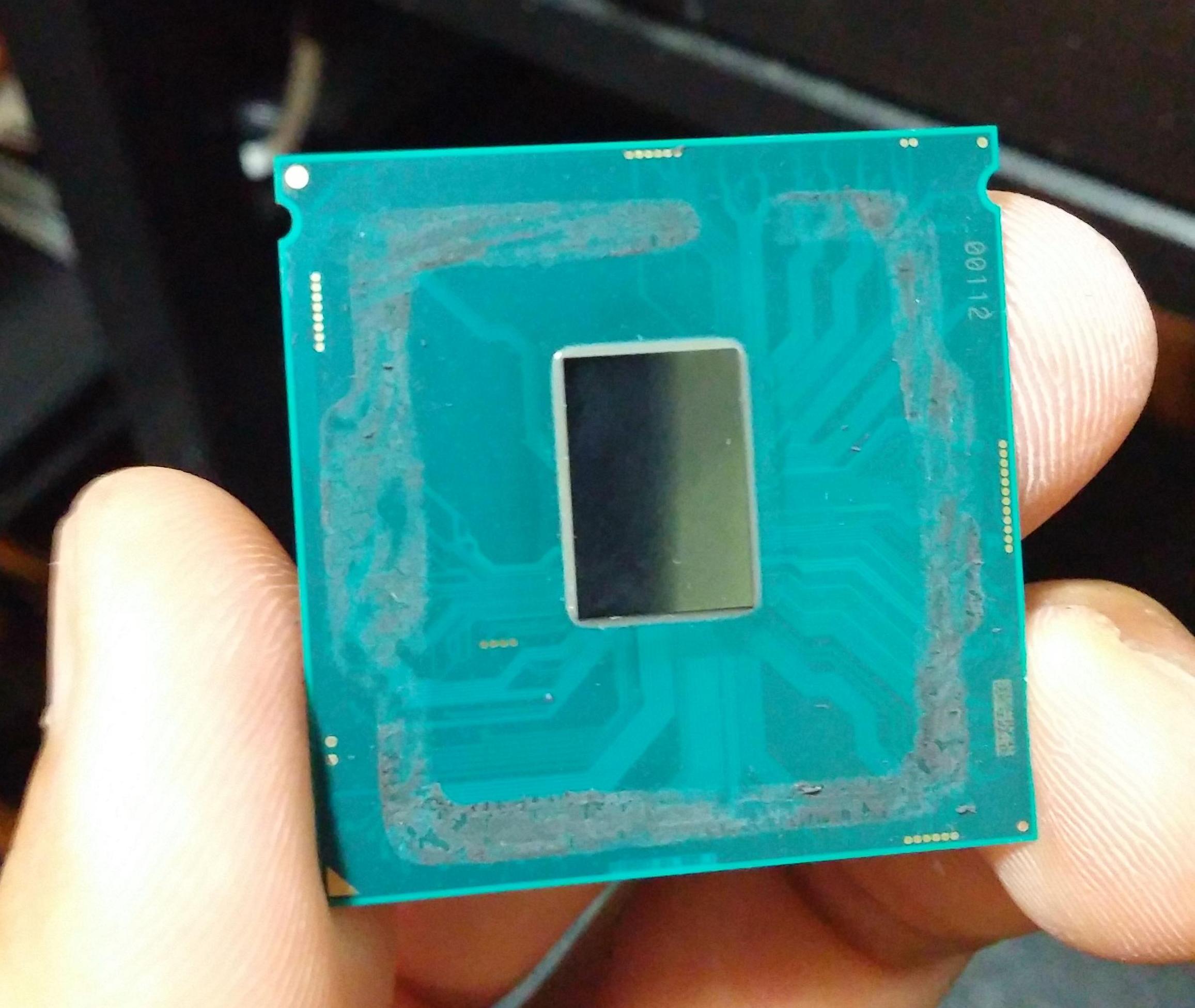
Image from Splave
First up is an image of the Skylake i7 silicon die on package. With our trusty interpolation measuring skills, the die area for the GT2 enabled quad core system comes out at 9.05 mm by 13.52 mm, or 122.4 square mm. Let's put this into perspective with other dies:
| CPU Specification Comparison | |||||
| CPU | Process Node |
Cores | GPU | Transistor Count (Schematic) |
Die Size |
| Intel Skylake GT2 4C | 14nm | 4 | GT2 | ? | 122.4mm2 |
| Intel Broadwell-H GT3e 4C | 14nm | 4 | GT3e | ? | ? |
| Intel Haswell-E 8C | 22nm | 8 | N/A | 2.6B | 356mm2 |
| Intel Haswell GT2 4C | 22nm | 4 | GT2 | 1.4B | 177mm2 |
| Intel Haswell ULT GT3 2C | 22nm | 2 | GT3 | 1.3B | 181mm2 |
| Intel Ivy Bridge-E 6C | 22nm | 6 | N/A | 1.86B | 257mm2 |
| Intel Ivy Bridge 4C | 22nm | 4 | GT2 | 1.2B | 160mm2 |
| Intel Sandy Bridge-E 6C | 32nm | 6 | N/A | 2.27B | 435mm2 |
| Intel Sandy Bridge 4C | 32nm | 4 | GT2 | 995M | 216mm2 |
| Intel Lynnfield 4C | 45nm | 4 | N/A | 774M | 296mm2 |
| AMD Trinity 4C | 32nm | 4 | 7660D | 1.303B | 246mm2 |
| AMD Vishera 8C | 32nm | 8 | N/A | 1.2B | 315mm2 |
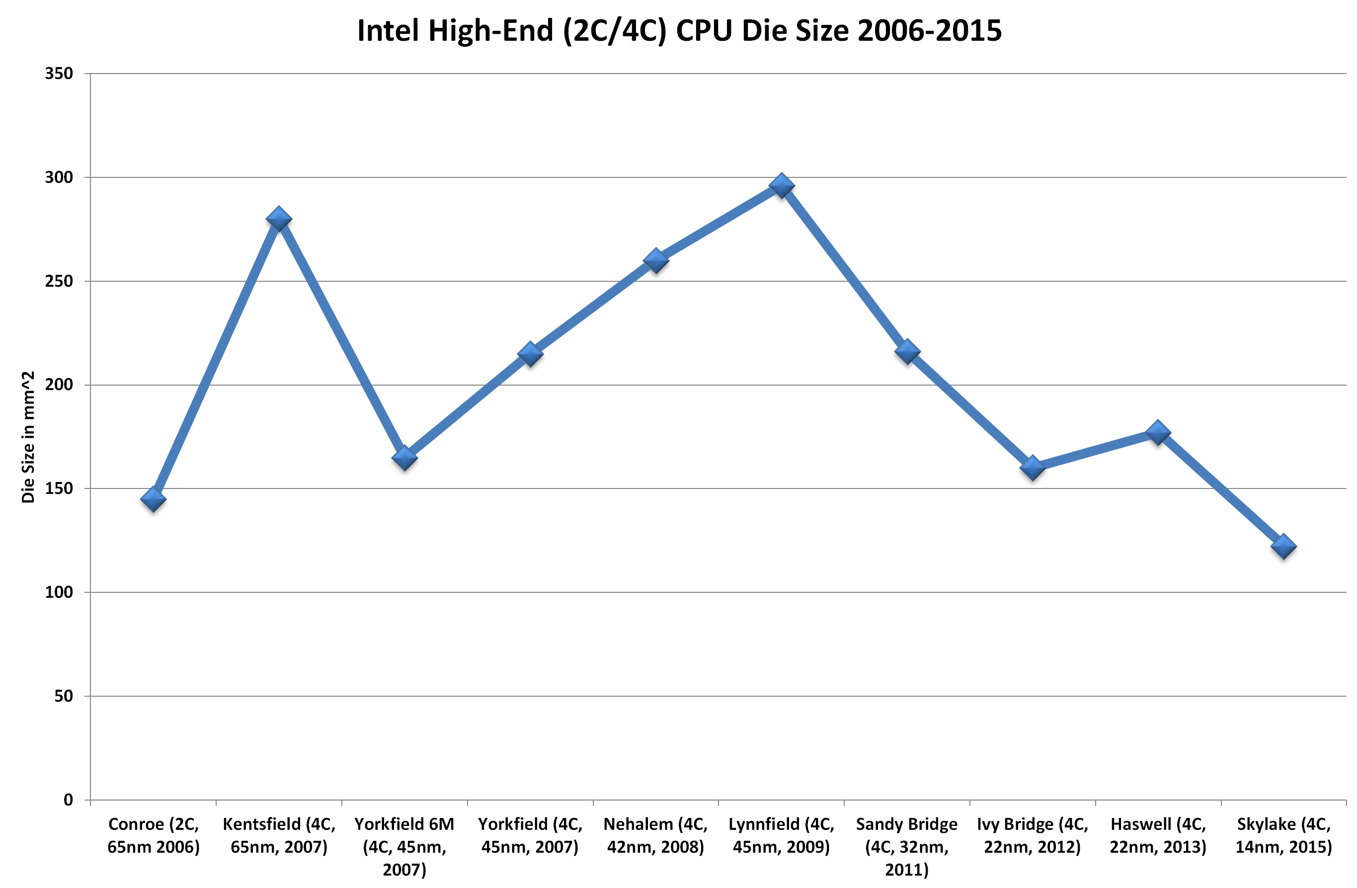
This makes Skylake the smallest die size for a quad core desktop processor from Intel we have seen, and that is including the integrated graphics in that calcualtion. Depending on the exact architectural details, previously in Haswell the die area was a near even split for cores and graphics after the L3 cache and IO functions (PCIe, Memory, DMI) were removed.
We won't know exact transistor numbers until they are disclosed at Intel's Developer Forum in mid-August, as well as a false color image die shot to show how much die area the main parts of the architecture are using. Although given the similarity to Haswell in terms of feature set (it seems to be similar with a few minor additions such as fixed function units, slightly different libraries, dual memory channels, DMI 3.0, etc.), if we take the number of transistors that GT2 Haswell had (1.4 billion) and put them in the die area we measure from the image, this comes out to a 11.4 million transistors per mm2.
Die size aside, Skylake also has a substantially thinner package than Devil's Canyon:
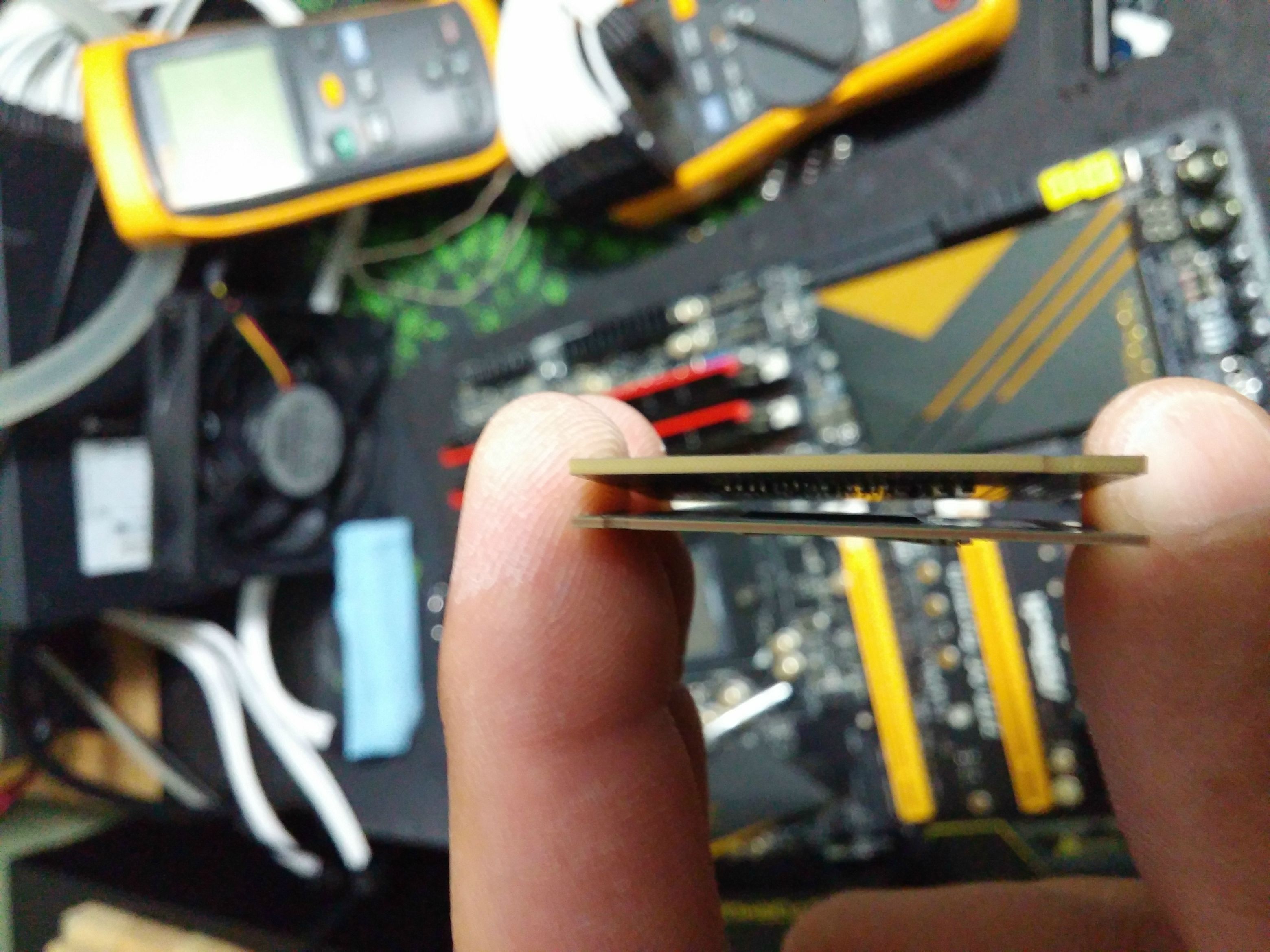
Image from Splave
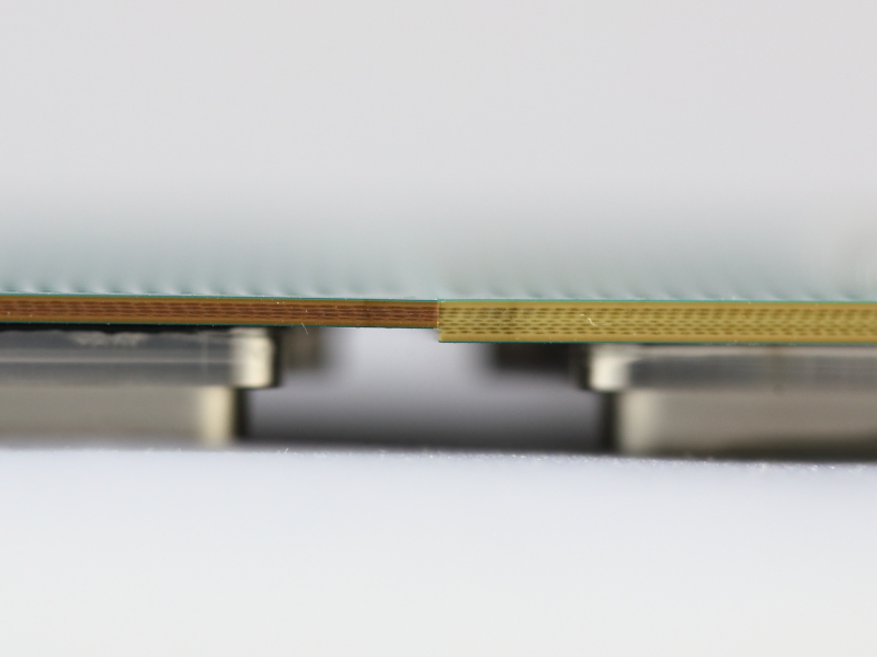
Image from PCWatch
According to PCWatch, the package thickness of the Core i7-4770K is 1.1mm, compared to 0.8mm for Skylake. This is a direct result of using fewer PCB layers, and here we count five for Skylake and eight for Haswell.
There could be several reasons for this. The removal of the fully integrated voltage regulator (FIVR) might reduce the number of PCB layers for power planes. The nature of the 14nm die might facilitate a thinner package as well. The cynical answer is that it is used to drive down cost. In the motherboard industry, a PCB with more layers is substantially more expensive but simplifies design when there are more features - there's also a side argument if more layers or fewer layers is better for overclocking. If we transplant this thinking to the processor, it becomes a balance of cost vs. complexity. Either way, the retail price of the processor is still relatively consistent with the previous iterations. Another thought to add to the mix would be if Intel has plans in the works to launch higher end processors based on Skylake (Kaby Lake?) in the future. The slight change in Intel's processor naming scheme (4770K to 6700K, as in 70K to 00K) also points to the potential move later in the lifetime of the product. The only hint in the naming scheme from Intel is that the 'processor numbering reflects that these processors belong to the 6th Gen Intel Core family'.
The thinness of the package has implications for removing the lid/heatspreader of the processor as well. Splave notes that previous heatspreader methods involving force, such as vices that were common during Haswell's tenure, may not be appropriate due to the thinness of Skylake. Splave shows an image of a failed attempt by another user on a Skylake CPU:
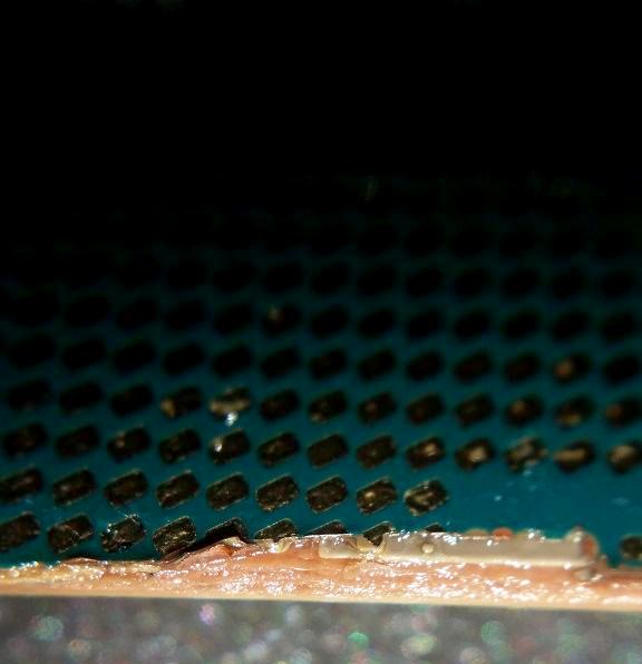
Image from Splave
Instead, a razor method (and something warm such as a hairdryer or the bean bags that iFixit uses to warm up glue in smartphones to take them apart) to cut through the black adhesive between the package and the IHS is suggested and it what was used for the CPU above. As there are no FIVR resistors to worry about on the top of the package, the first resistance a razor blade will encounter after the black adhesive is the silicon die itself. All that being said, over at PCWatch they successfully have used a vice method.
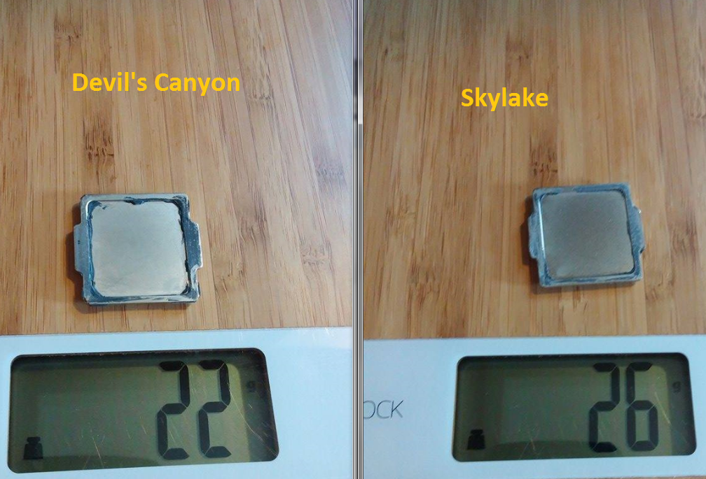
Image from Splave
Interestingly the heatspreader for Skylake is heavier than that from Haswell by nearly 20%, moving up from 22g to 26g. Given the copper mass that usually sits on a high end processor this should not matter much, although basic aluminium coolers might see a small benefit here by virtue of the minor extra mass. This might also just be that the mounting requirements for Haswell and Skylake are the same, and the extra mass comes from the added z-height required to maintain the mounting as before.
So why are we talking about removing the heatspreader? Back with Haswell (as well as Ivy Bridge to a degree), it was discovered that the thermal interface material between the silicon die and the heatspreader was both an insufficient amount and lower quality than previous generations, as well as the heatspreader being far away from the CPU due to the black adhesive, causing more air bubbles and poorer heat transfer than is optimal. For a stock processor, this difference has little effect to the use of the system, but for overclockers it meant that they were more thermally limited than silicon limited with their overclocking.

Image courtesy of Idontcare
Devil's Canyon changed that - here was a better binned Haswell processor with a higher quality package, giving a ten degrees cooler system at load. It is worth noting that previously on certain platforms Intel had been providing a mixed metal interface (generalized as a soldered interface) between the silicon and the heatspreader, which is the best but most expensive option. If the cost of the interface is reduced by 0.1 cents, then that's a significant saving on millions of processors. Devil's Canyon was a small subset of sales, so spending that extra for that specific crowd could be seen as beneficial to Intel's perspective by overclockers.
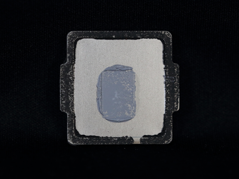
Image from PCWatch
To paraphrase Splave again, he comments that the thermal paste (TIM)o n his Skylake is certainly worse than that of Devil's Canyon. If the extra mass on the IHS is coming from a taller heatspreader (by virtue of the smaller package substrate), then more TIM is needed otherwise there will be substantial air bubbling of the TIM between the CPU and the heatspreader. By replacing his own thermal paste and resecuring the heatspreader, he saw an 18°C drop in temperatures at his highest air overclock with the old paste (5.1 GHz at 1.48 volts) - from 96ºC that overheated to 78ºC on the warmest core. An 18°C drop is immense. Under those conditions, and based on rough testing not published in our Skylake review, it could equal another 100-400 MHz depending on the quality of the processor. PCWatch confirms that switching out the paste with CoolLaboratory’s Liquid Pro (a liquid metal adhesion interface) reduced temperatures at 4.6 GHz from 88ºC to 68ºC

Image from PCWatch
This throws up some questions - is this just a result of design decisions for cost, or is there a Devil's Canyon type processor coming later in the design cycle?
Source: Overclock.net, PCWatch


86 Comments
View All Comments
Ryan Smith - Monday, August 10, 2015 - link
The risk is cracking your CPU die. It's not guaranteed, but these CPUs are capped with an IHS for a reason.DanNeely - Monday, August 10, 2015 - link
The top of the die being closer to the mobo than the top of the heat spreader will prevent a lot of heatsink mounting designs from being able to make contact; and you're back in the world of 15 years ago where a botched heat sink install can crush the (edge of the) core and ruin the chip.ShieTar - Monday, August 10, 2015 - link
Well, it will no longer spread the heat; so don't do this if you have cooler with a direct heat-pipe design, your heat source may end up between two heat-pipes.Also you take a bigger risk of damaging the CPU while installing the cooler. Nevertheless, some people have done exactly what you are talking about, and MSI have even designed a "Die Guard" support plate for exactly this purpose:
http://www.madshrimps.be/articles/article/1000656/...
MrSpadge - Tuesday, August 11, 2015 - link
A "heat spreader" is just copper. It doesn't spread the heat any better than the copper base of a good heat sink, irregardless of heat pipe placing. The issue of mechanical protection is real, though.ImSpartacus - Monday, August 10, 2015 - link
Based on Ian's graph, these die are getting smaller and smaller and yet their TDPs aren't getting lower. So there's a heat density problem. I wonder if the IHS helps mitigate that.On the flip side, if the IHS is off, then you can see exactly where the die is and place your thermal paste appropriately on these increasingly asymmetrical chips (5775C?). And you know for sure that there's no shitty material between the die and the IHS. You have more control over overclocking success.
And then there's always the durability argument. The IHS protects the fragile die.
CaedenV - Monday, August 10, 2015 - link
I wonder how true this is. Sure the TDP remains the same... but these onboard GPUs are getting monstrous in size, and grow 20-50% each generation. My bet is that the CPU TDP is continually shrinking, and then they fill up the remaining TDP budget with as much GPU as they can. For those of us who rarely (if ever) touch the GPU on these chips it should not be a huge concern.Gigaplex - Monday, August 10, 2015 - link
Benchmarks showing power usage of just the CPU portion says otherwise. The CPU component alone can consume the entire TDP.ImSpartacus - Monday, August 10, 2015 - link
Sure it could, but will it? Client workloads have plateaued, but Intel churns out a predictable 5ish% performance bump every year.It's always nice to have legroom for those unusual circumstances when your cpu needs to "race to sleep", but it's a diminishing returns kind if thing because the use case is already pretty well satisfied.
ImSpartacus - Monday, August 10, 2015 - link
You're probably right.Intel sends to care about gpus now.
MrSpadge - Tuesday, August 11, 2015 - link
That's true for the 6700K and any E series CPU. The regular Skylakes will have 65 W TDPs at most, which is easy to cool and about the same power density as previous designs.BTW: this issue of "where to apply thermal paste" sounds really strange. "Back in the day" you tried not to make a small dot of thermal paste exactly where the chip is, you tried to cover the entire surface with a thin layer. If Ian sees 15+°C too high temperatures with his pea dot method, I would say the pea was simply too small rather than in wrong spot.