Qualcomm Details The Snapdragon 888: 3rd Gen 5G & Cortex-X1 on 5nm
by Andrei Frumusanu on December 2, 2020 10:00 AM EST- Posted in
- Mobile
- Qualcomm
- Smartphones
- SoCs
- 5G
- Cortex A78
- Cortex X1
- Snapdragon 888
Triple ISPs: Concurrent Triple-Camera Usage
Interestingly enough, during yesterday’s keynote event, Qualcomm described themselves as a camera company, which is a funny way to see things, but actually somewhat makes sense given the large leaps in smartphone camera capture capabilities over the recent years.
The new Snapdragon 888 pushes the envelope in terms camera abilities by adding a whole new independent third ISP to the SoC, allowing the SoC to now run three independent camera modules concurrently, opening up new use cases for vendors and camera applications.

The new triple-ISP architecture now increases the overall pixel processing throughput by 35% to 2.7Gigapixels/s, allowing for concurrent usage of up to three 28MP sensors with zero shutter lag captures. Alternatively, you can use a combination of 64+25MP sensors with ZSL, or a single 84MP sensor with ZSL. There’s still also support for ultra-high-resolution sensors up to 200MP, but image captures here don’t support ZSL.
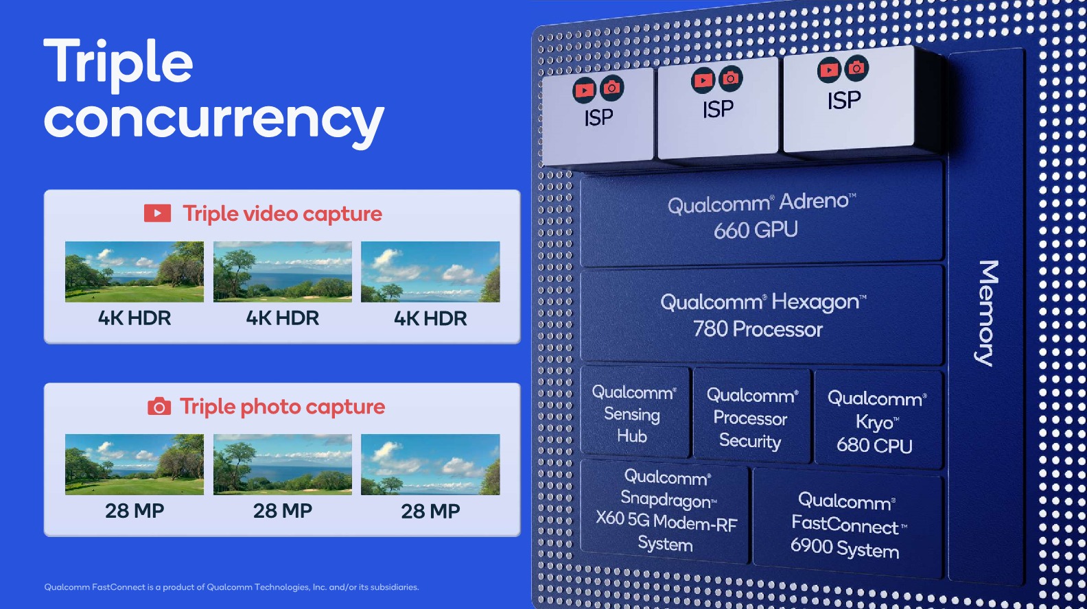
Allowing concurrent captures of three sensors now allows for the holy trifecta of ultra-wide-angle, wide-angle and telephoto modules to capture a scene at the same time, allowing for more interesting use-cases such as image stitching and image fusion to happen to seamlessly.
One interesting capability that Qualcomm was advertising is triple-stream 4K HDR video recording. That’s a bit of an odd-ball use-case as I do wonder about the practical benefits, but I do at least hope that the new triple ISP system allows for more seamless switching and zooming in and out between the various camera modules during video recording.
Video recording capabilities this year don’t seem to have changed, compared to the Snapdragon 865. This means 4K120 or 8K30 are still the peak capture modes, supporting also slow-motion of 720p960. Formats are also unchanged, with HEVC encoding in HDR formats such as HDR10+ or Dolby Vision being supported.
AV1 decoding didn’t make the cut this year unfortunately, which means wide-spread adoption in mobile for the codec will be delayed for another year.
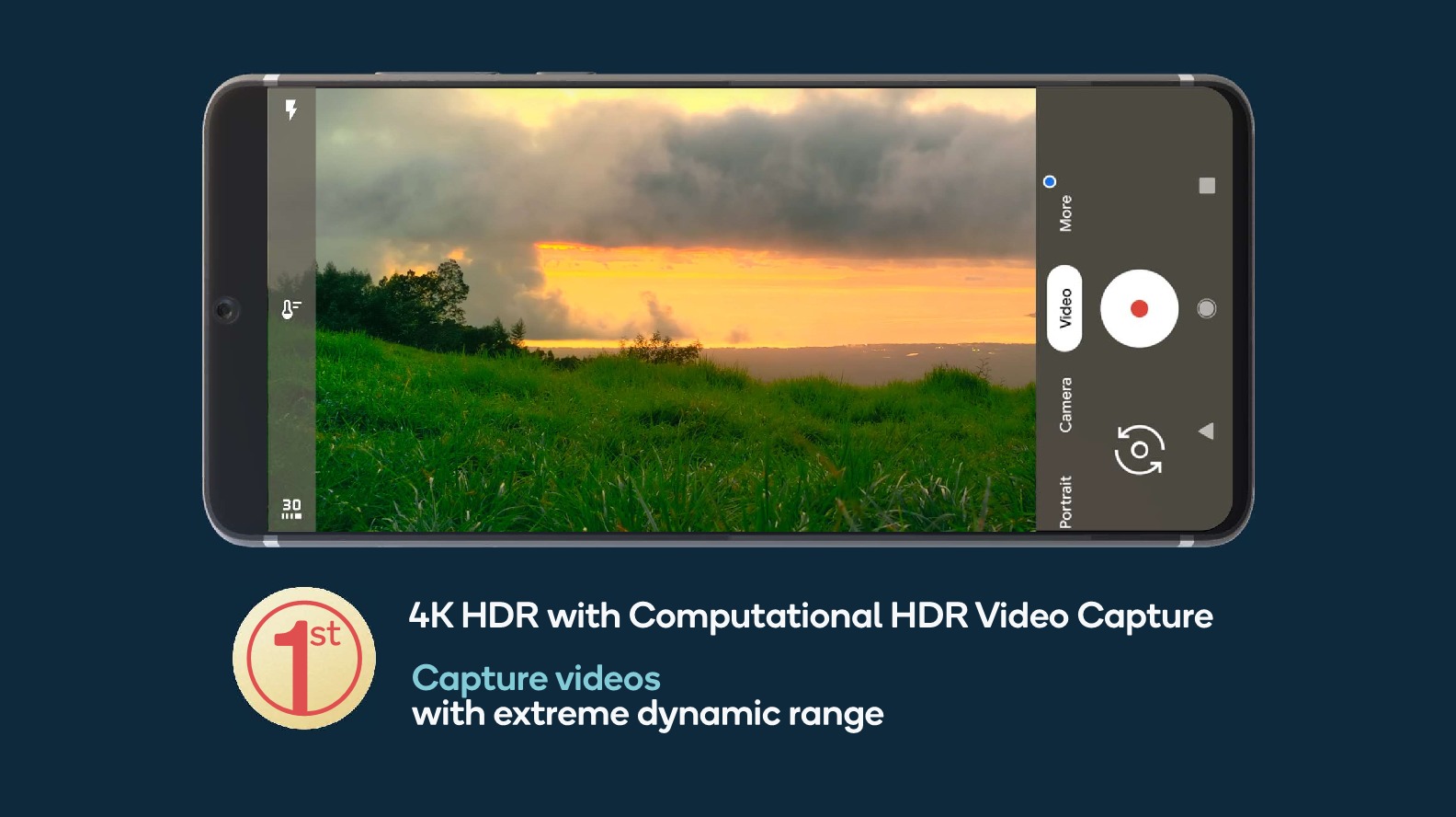
While the video encoding formats haven’t changed, the image processing capabilities for HDR capture has. Thanks to the new ISPs and the raw performance throughput, the new Snapdragon 888 will be able to capture 4K HDR footage with the more advanced computational HDR processing being applied on each and every frame of the video.
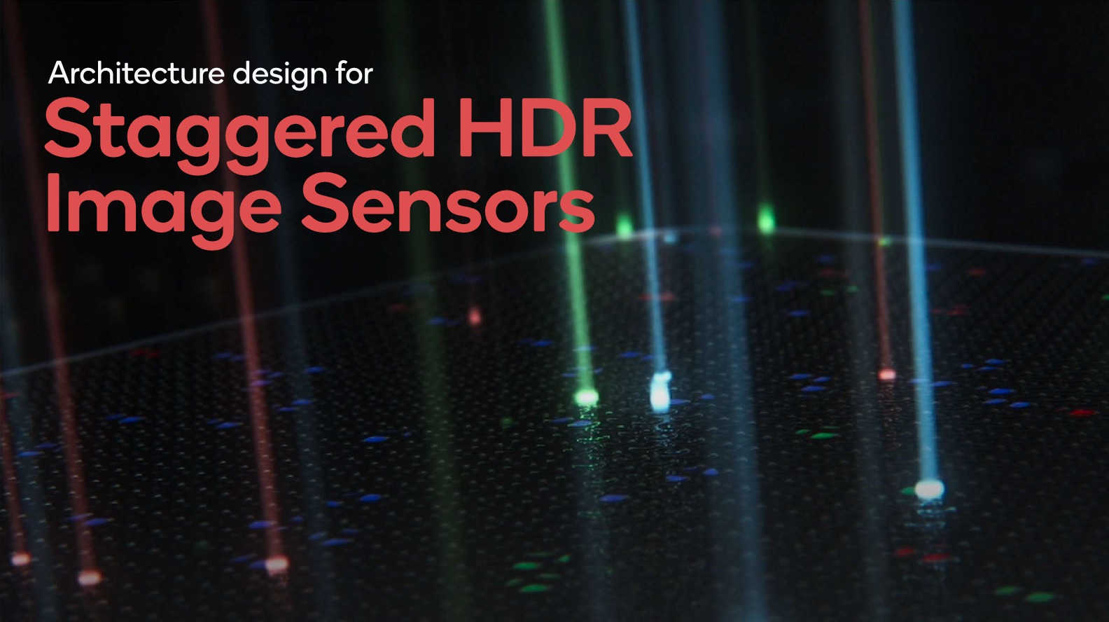
Qualcomm claims that the new ISP in the Snapdragon 888 is the first to support new next-generation staggered HDR sensors.
Source: OmniVision
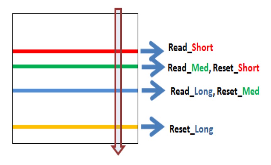
These are sensors that can have multiple rolling shutters, meaning sensor line readouts, active at the same time on the sensor. Instead of taking multiple exposures one at a time sequentially by scanning out the sensor matrix from start to finish, the sensor will start another exposure immediately after the completed line read-out, reducing the time in-between exposures greatly. This should allow for significant less motion ghosting between the exposures and a sharper resulting recombined HDR image capture than current generation sensors which only have a single active line readout on the sensor.
While we haven’t actually heard of such sensors from Samsung or Sony yet, Qualcomm is adamant that we’ll be seeing smartphones in 2021 employing this new technology.

A further improvement for still-picture captures is the advancement of the new multi-frame noise reduction engines inside of the ISPs. It’s said that the quality of the noise reduction has been improved this generation, allowing for even better low-light captures with the native capture mode (no computational photography).


123 Comments
View All Comments
eastcoast_pete - Wednesday, December 2, 2020 - link
Thanks Andrei! While not the or even a focus of your article (there was no need), I am struck by how stuck ARM bigLittle type designs are when it comes to the efficiency cores. A55, still? Let's make no mistake, you/we want capable and efficient small cores in the SoC, so that the big cores don't feast on the battery all the time. 5G modems tend to increase power use (this integrated one hopefully a bit less), so having the ability to stay on the low power cores of the CPU longer is even more important.Andrei, if you can, I'd appreciate a deeper dive into the state of the art of the small cores, especially a comparison of Apple's vs. stock ARM A55 designs. Thanks!
psychobriggsy - Wednesday, December 2, 2020 - link
I imagine that there's only so far you can take an in-order ARMv8 core design when you want to optimise for power consumption. ARM do release updates to their core designs, whilst retaining the same name as well, so they do get small improvements. There are no ISA changes for these consumer cores either, as far as I am aware.But it does look like the A55 has pretty much not changed much in several years, and simply become more and more efficient as the process has shrunk down to 5nm and the clocks have remained the same. I think people were expecting an A58 by now - maybe there will be an A59 to go with the A79 next year?
Lolimaster - Thursday, December 10, 2020 - link
Probably called A63.Ppietra - Wednesday, December 2, 2020 - link
This is what he said about the icestorm cores in the A14:"The performance showcased here roughly matches a 2.2GHz Cortex-A76 which is essentially 4x faster than the performance of any other mobile SoC today which relies on Cortex-A55 cores, all while using roughly the same amount of system power and having 3x the power efficiency."
brucethemoose - Wednesday, December 2, 2020 - link
Makes one wonder what on earth Apple is doing to achieve that. Its not like ARM's CPU architects are underpaid chumps.Some of it is extra die space, I guess? The LITTLE cores have to be, err, little, while Apple can afford to blow up area for efficiency.
tkSteveFOX - Wednesday, December 2, 2020 - link
Not really. Apple's chips are always roughly the same size as QC and Kirin top chips and on the same nodes.Just better architecture and more R&D investment. QC have been doing the same chip for 3 gens now, just updating the ARM tech and gains in AI and ISP, but the CPU config remains the same, it's even clocked the same!
Ppietra - Wednesday, December 2, 2020 - link
I think Apple CPU cores are significantly bigger than ARM designsheadeffects - Wednesday, December 2, 2020 - link
I don’t have all the numbers on me but Apple has never had an on die modem while Qualcomm usually does, so you can’t directly compare die sizes like that. Andrei would perhaps know the measurements of the actual core sizes and how they compare from Apple to Qualcomm.Fulljack - Thursday, December 3, 2020 - link
Nope. Apple A13 is 98,48 mm² while Snapdragon 865 is 83,54 mm²—according to TechInsights. Both are manufactured on TSMC N7P and feature no integrated modem. So yeah, wider (and thus bigger) cores design does improve performance, but not always though.RSAUser - Wednesday, December 2, 2020 - link
Apple has both an architecture design leas and a process node lead, TSMC 5nm vs Samsungs Marketing Version of it which is worse than TSMC 7nm.