Arm Announces Mobile Armv9 CPU Microarchitectures: Cortex-X2, Cortex-A710 & Cortex-A510
by Andrei Frumusanu on May 25, 2021 9:00 AM EST- Posted in
- SoCs
- CPUs
- Arm
- Smartphones
- Mobile
- Cortex
- ARMv9
- Cortex-X2
- Cortex-A710
- Cortex-A510
The Cortex-A710: More Performance with More Efficiency
While the Cortex-X2 goes for all-out performance while paying the power and area penalties, Arm's Cortex-A710 design goes for a more efficient approach.
First of all, the new product nomenclature now is self-evident in regards to what Arm will be doing going forward- they’re skipping the A79 designation and simply starting fresh with a new three-digit scheme with the A710. Not very important in the grand scheme of things but an interesting marketing tidbit.
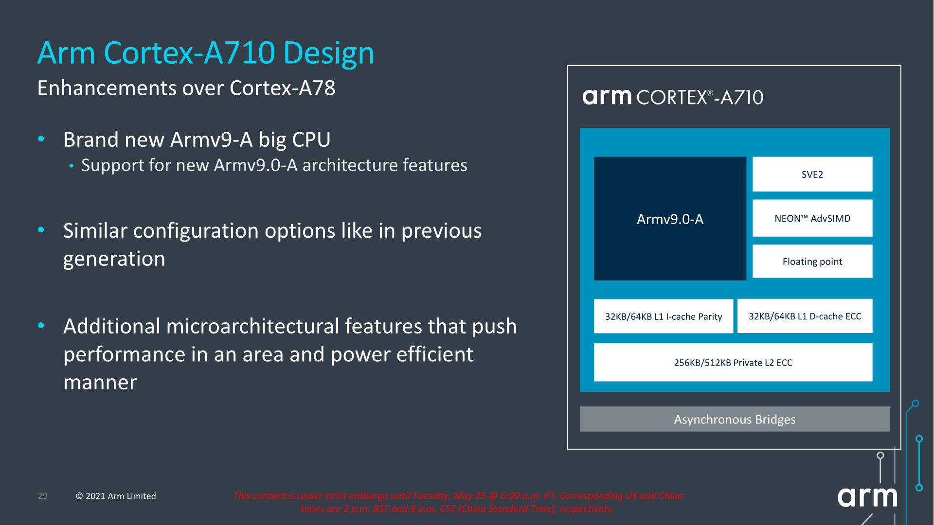
The Cortex-A710, much like the X2, is an Armv9 core with all new features that come with the new architecture version. Unlike the X2, the A710 also supports EL0 AArch32 execution, and as mentioned in the intro, this was mostly a design choice demanded by customers in the Chinese market where the ecosystem is still slightly lagging behind in moving all applications over to AArch64.
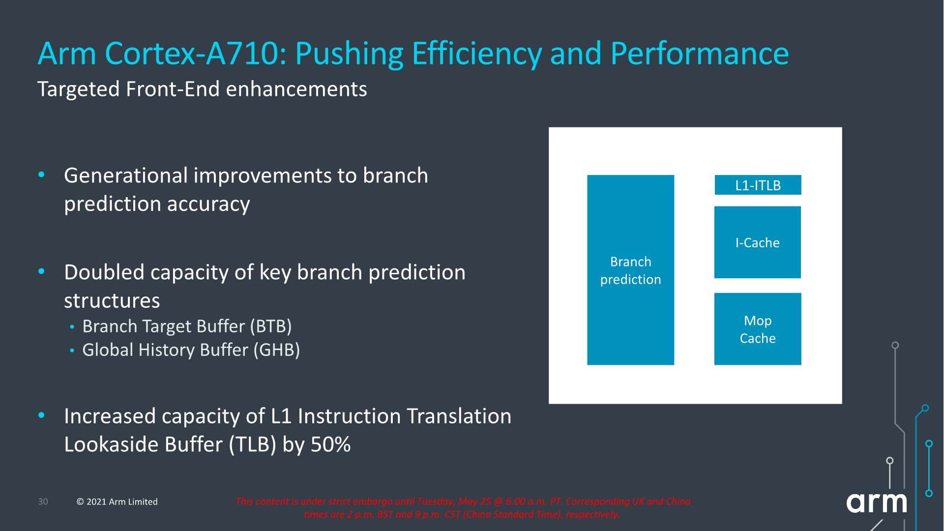
In terms of front-end enhancements, we’re seeing the same branch prediction improvements as on the X2, with larger structures as well as better accuracy. Other structures such as the L1I TLB have also seen an increase from 32 entries to 48 entries. Other front-end structures such as the macro-OP cache remain the same at 1.5K entries (The X2 also remains at 3K entries).
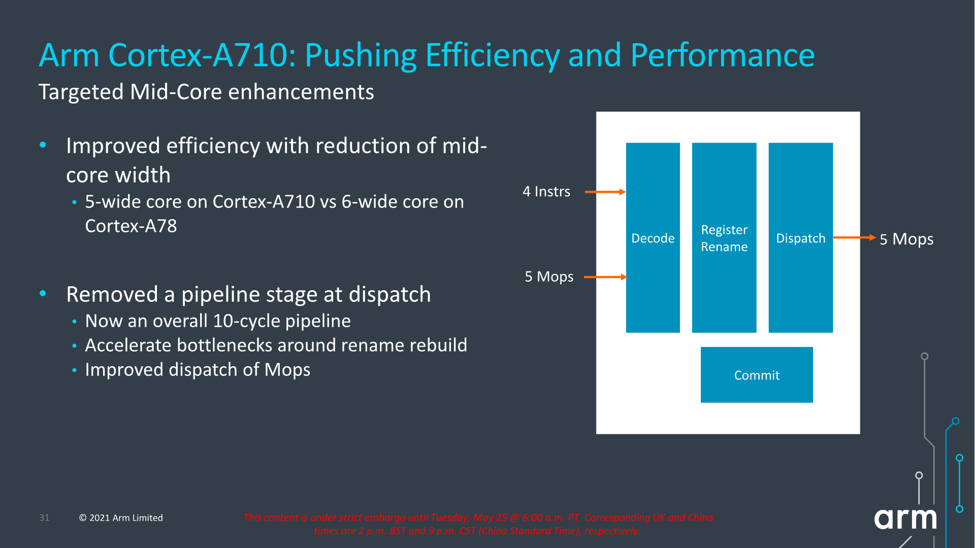
A very interesting choice for the A710 mid-core is that Arm has reduced the macro-OP cache and dispatch stage throughputs from 6-wide to 5-wide. This was mainly a targeted power and efficiency optimization for this generation, as we’re seeing a more important divergence between the Cortex-A and Cortex-X cores in terms of their specializations and targeted use-cases for performance and power.
The dispatch stage also features the same optimizations as on the X2, removing 1 cycle from the pipeline towards an overall 10-cycle pipeline design.
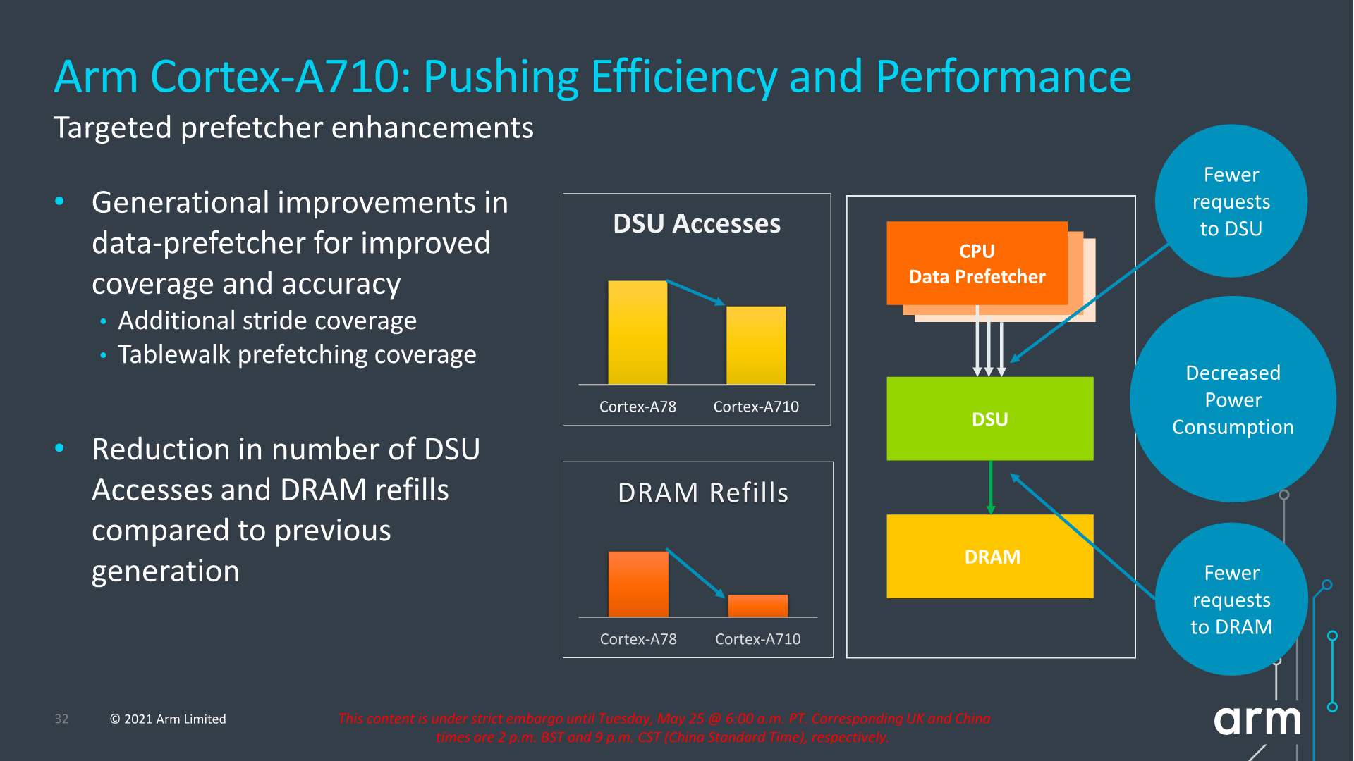
Arm also focuses on core improvements that affect the uncore parts of the system, which take place thanks to the new improvements in the prefetcher designs and how they interact with the new DSU-110 (which we’ll cover later). The new combination of core and DSU are able to reduce access from the core towards the L3 cache, as well as reducing the costly DRAM accesses thanks to the more efficiency prefetchers and larger L3 cache.
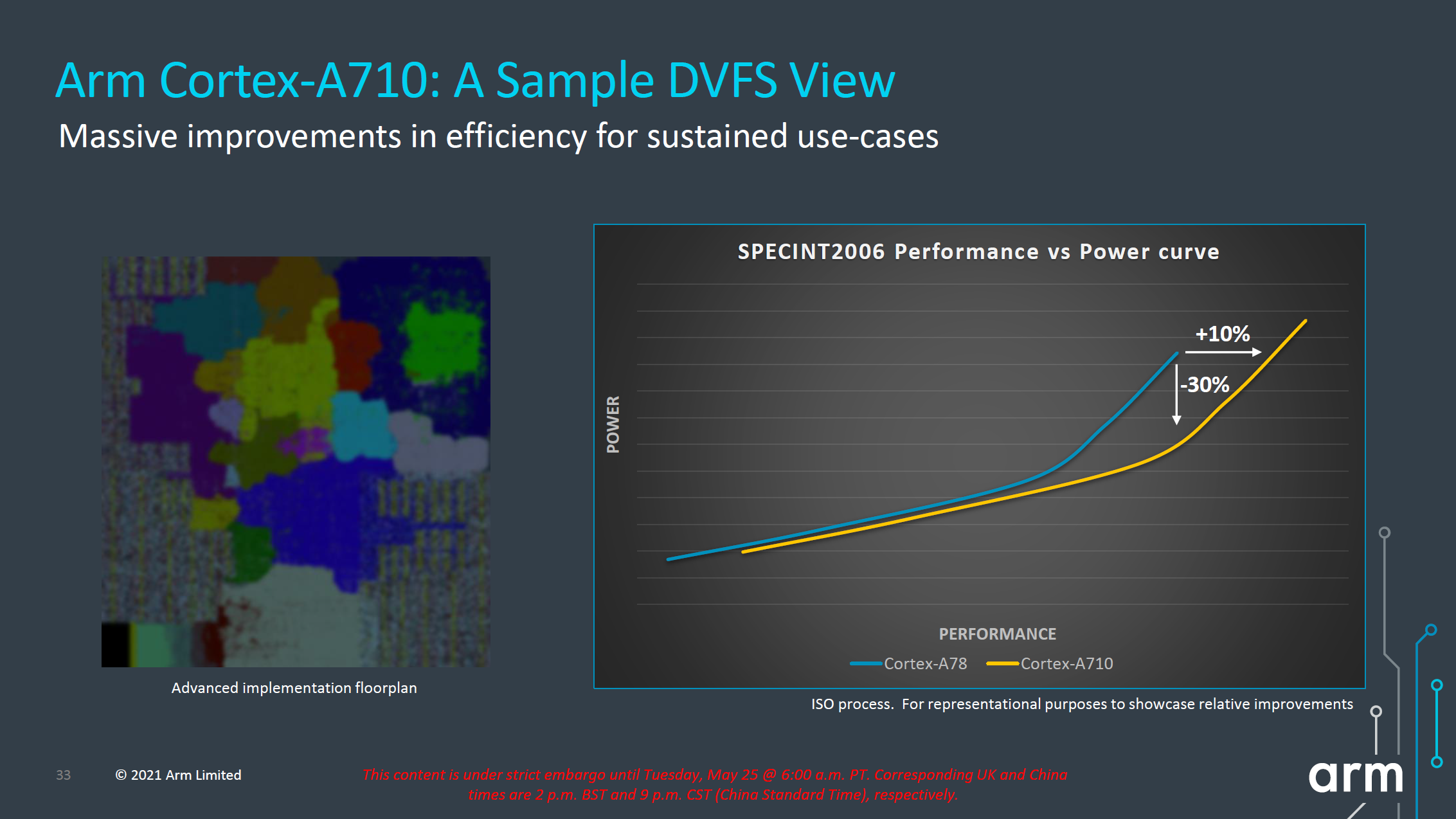
In terms of IPC, Arm advertises +10%, but again the issue with this figure here is that we’re comparing an 8MB L3 cache design to a 4MB L3 cache design. While this is a likely comparison for flagship SoCs next year, because the Cortex-A710 is also a core that would be used in mid-range or lower-end SoCs which might use much smaller L3 caches, it’s unlikely we’ll be seeing such IPC improvements in that sector unless the actual SoCs really do also improve their DSU sizes.
More important than the +10% improvement in performance is that, when backing off slightly in frequency, we can see that the power reduction can be rather large. According to Arm, at iso-performance the A710 consumes up to 30% less power than the Cortex-A78. This is something that would greatly help with sustained performance and power efficiency of more modestly clocked “middle” core implementations of the Cortex-A710.
In general, both the X2 and the A710’s performance and power figures are quite modest, making them the smallest generation-over-generation figures we’ve seen from Arm in quite a few years. Arm explains that due to this generation having made larger architectural changes with the move to Armv9, there has been an impact in regards to the usual efficiency and performance improvements that we’ve seen in prior generations.
Both the X2 and the A710 are also the fourth generation of this Austin microarchitecture family, so we’re hitting a wall of diminishing returns and maturity of the design. A few years ago we were under impression that the Austin family would only go on for three generations before handing things over to a new clean-sheet design from the Sophia team, but that original roadmap has been changed, and now we'll be seeing the new Sophia core with larger leaps in performance being disclosed next year.


181 Comments
View All Comments
jeremyshaw - Tuesday, May 25, 2021 - link
Something I'm not quite catching with the DSU, does it allow for different configurations that we've already seen? Something like the 8xA78C we saw announced a while back?jeremyshaw - Tuesday, May 25, 2021 - link
*than, sorrySarahKerrigan - Tuesday, May 25, 2021 - link
They show 8x X2 configs, so I'd be shocked if 8xA710 was not also on the menu.igor velky - Tuesday, May 25, 2021 - link
first two slides on page 5 will give you answer,both slides show cpu cores inside one cpu cluster
first slide shows different cores,
second shows only one type of core in cpu cluster
on page 6 because of bad formatting there are two slides looking like one picture
so second slide, bottom half of first picture
shows you that you can put max 8 cpu clusters to one chip.
so you can have
max 8 cpu cores per cpu cluster
times
8 cpu clusters per one chip.
you choose cores, you choose how many cores, you choose which type of cores, you choose how many memory channels, you choose how many and what type of additional accelerators you put inside chip...
because youre apple, samsung, qualcomm...
and you choose this things and let someone to "etch it" into silicon.
and you then sell it.
melgross - Tuesday, May 25, 2021 - link
Well, Apple doesn’t “choose” cores, they design them from scratch.Linustechtips12#6900xt - Wednesday, May 26, 2021 - link
ehhh, they get the IP for cores like the x1 or a76 then they tweak them either a lot or a little and create their current "firestorm/Icestorm" coresmichael2k - Wednesday, May 26, 2021 - link
Sure, they tweak them a lot, just like I tweaked your post a lot to make my own. The A13 released in 2019 was an 8 wide CPU; in comparison the state of the art A76 at the time was only a 4 wide CPU. That’s a pretty big deal.The X1 has an 8 wide dispatch, meaning it can issue 8 Mops per cycle but only decode 5 instructions per cycle. This is 2 years after Apple released the A13 which was 8 wide dispatch and decode. If you look at Anandtech’s A14 article you see that Apple has made the Icestorm cores roughly equivalent to an A76 since it is a 3 wide out of order design.
You can read more here:
https://www.anandtech.com/show/16226/apple-silicon...
mattbe - Wednesday, May 26, 2021 - link
This is complete BS. They license the ISA from ARM. They DO NOT USE OR TWEAK cores like the X1 and A76 to create their firestorm/ice storm cores. These are information that can easily be verified so it's pretty ignorant for you to make those claims.FunBunny2 - Wednesday, May 26, 2021 - link
" They DO NOT USE OR TWEAK cores"near as I can tell, most 'innovation' in cpu design/engineering has been, for years, throwing ever expanding transistor budgets (can we expect that to continue?) at register width, path width, buffer/cache width and number, pulling off-chip function on-chip. and the like. if Apple should ever publish the full spec of one of these chips, will we see that they've done anything more 'innovative' than Bigger, Wider, More?
all of the 'innovation' cited by michael2k fits that bill.
mode_13h - Thursday, May 27, 2021 - link
> if Apple should ever publish the full spec of one of these chips,> will we see that they've done anything more 'innovative' than Bigger, Wider, More?
You don't get perf/W numbers like Apple's by simply doing "bigger, wider, more".
There's information out there about some of their tricks, if you're willing to look for it. But I understand that it takes work and why do that, when you're perfectly content in your belief that there's nothing new under the sun?