Intel Details PowerVia Chipmaking Tech: Backside Power Performing Well, On Schedule For 2024
by Ryan Smith on June 5, 2023 9:00 AM EST- Posted in
- CPUs
- Intel
- EUV
- IFS
- Intel 20A
- Intel 18A
- PowerVIA
- Arrow Lake
- Backside Power
- Crestmont
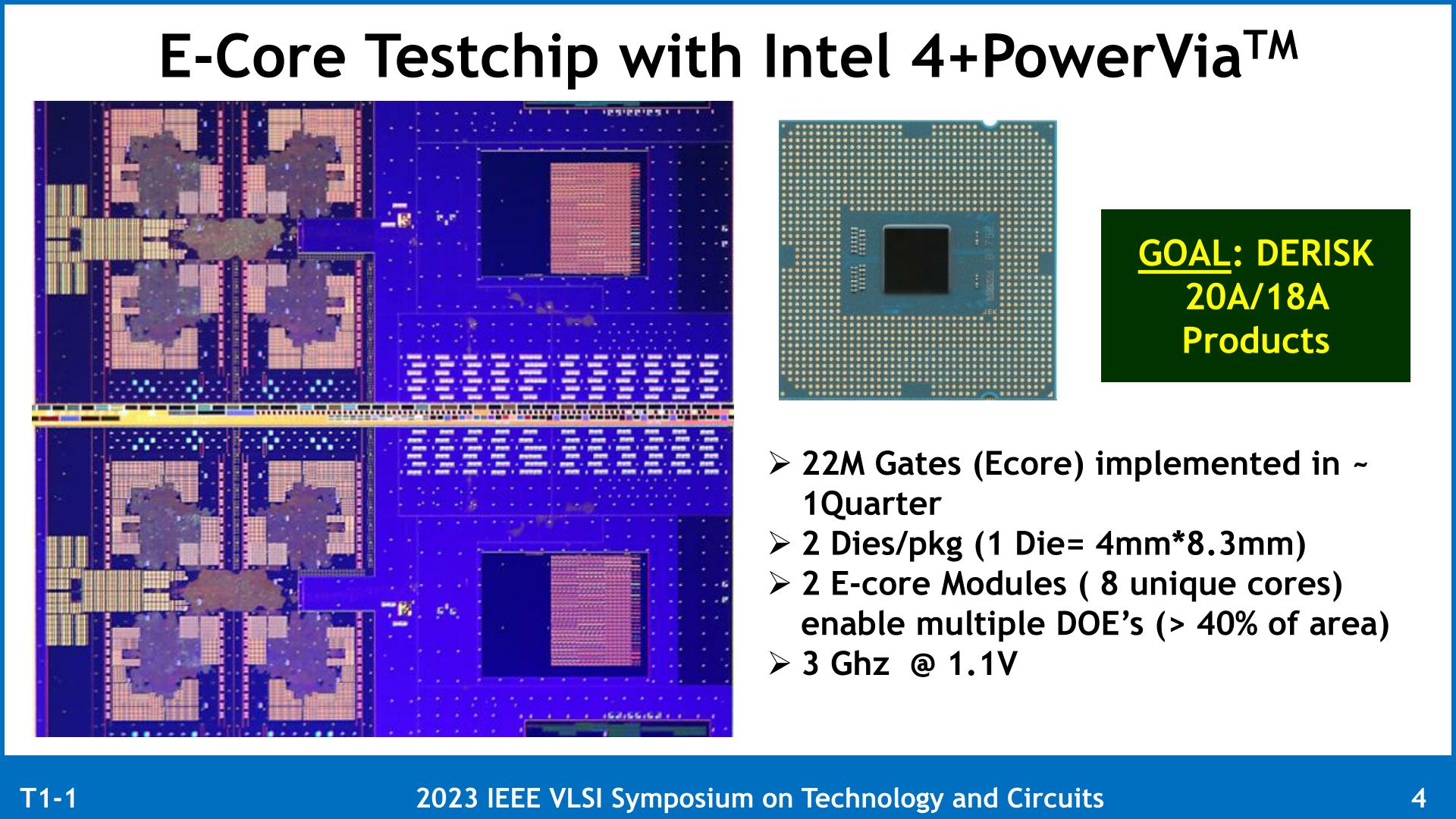
Blue Sky Creek: An Intel 4 + PowerVia Test Chip, Based on Crestmont E-Cores
To put PowerVia to the test and to prove that it’s working as expected, Intel’s validation vehicle for the technology is a chip they’re calling Blue Sky Creek.
Derived from Intel’s Meteor Lake platform, Blue Sky Creek uses two dies of E-cores that are based on Intel’s Crestmont CPU architecture. The reason Intel is using Crestmont here is two-fold: first, it was originally designed for Intel 4, making it a good candidate for porting over to the Intel 4 + PowerVia process. And second, because E-cores are tiny; the quad-core test dies are just 33.2mm2 (4mm x 8.3mm) in size, making them a good balance between complexity for testing and not having to actually yield a massive die on an experimental process node.
Intel isn’t focused too much on the performance of the E-cores in Blue Sky Creek. But they do note that the designed frequency was 3GHz at 1.1v.
With regards to the bigger picture, Big Sky Creek’s existence is part of Intel’s grand plan to mitigate the risk of introducing two major technological changes within the same process node – a problem that hit Intel rather hard with the overly-ambitious development plan for their 10nm (Intel 7) process node.
As outlined by the company back in 2022, of the two technologies, PowerVia was considered the riskier of the two. For that reason, Intel would be developing an interim test node just for PowerVia, allowing them to work on the technology separately from RibbonFETs. Ultimately, if PowerVia development had not progressed as expected, Intel could still do RibbonFET development, and bring out chips sans-PowerVia.
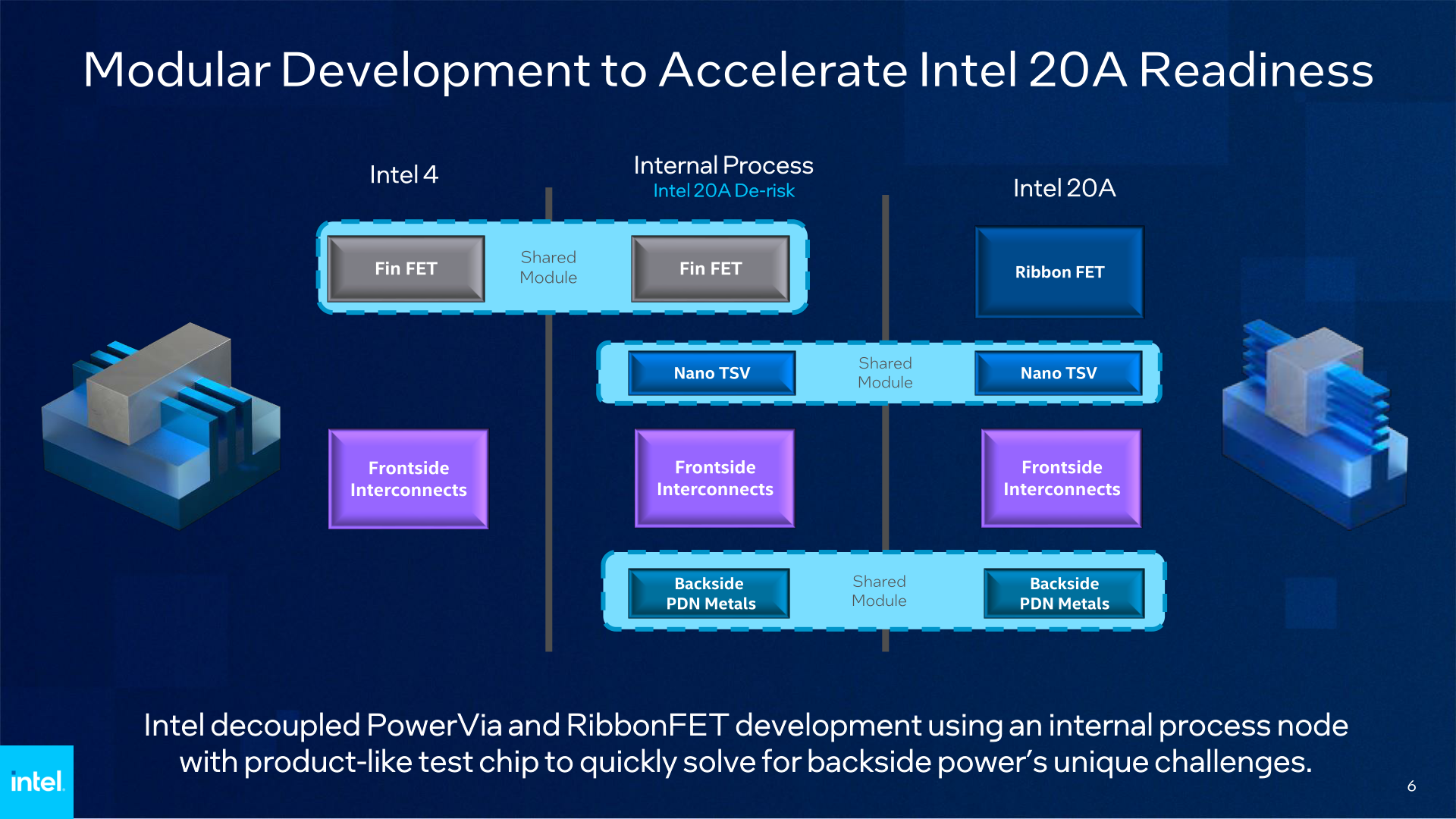
For similar reasons, you won’t find much discussion of RibbonFET from Intel for the VLSI conference. While it’s an important technology for the company, it’s essentially a sure-thing for Intel. The company won’t even be the first fab with GAAFET technology, so while RibbonFET does come with its own challenges, intel didn’t need to prepare any risk mitigation strategies for it in the same way as they did PowerVia.
PowerVia In Practice: Intel’s Finds 30% Reduction in IR Droop, 6% Higher Clockspeeds, Ready for HVM
Diving into the results of Intel’s PowerVia papers, the company has broken out their results for Blue Sky Creek on a metric-by-metric basis, looking at everything from chip density to performance to thermals.
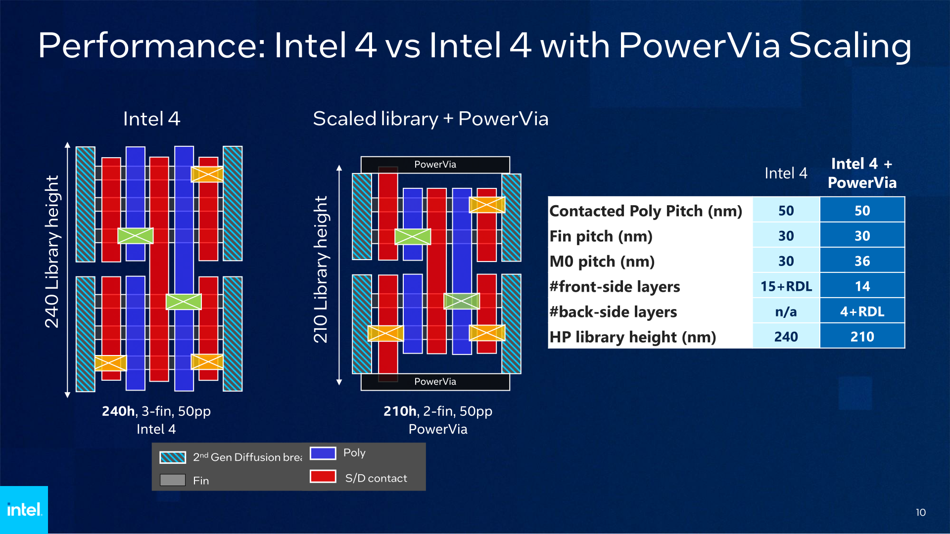
Starting with chip density, here’s a look at the size of the high performance (HP) library cells that Intel developed and fabbed for their test chip, and how those cells compare to the equivalent Intel 4 cells. As noted earlier, the shift to PowerVia has allowed Intel to relax the pitch of the critical M0 metal layer, enlarging it from 30 nm to 36 nm. The other major parameters of the node, such as the fin pitch and contacted poly pitch (CPP) remain at 30 nm and 50 nm respectively.
Yet, those changes, combined with Intel’s ability to reduce the number of fins in use from 3 to 2, result in an overall smaller cell. Thanks to PowerVia, Intel was able to bring the library height down to 210 nm, from 240 nm on Intel 4. And with the CPP holding constant at 50 nm, that means the overall cell size has been reduced by 12.5%, despite not using a formally “denser” node.
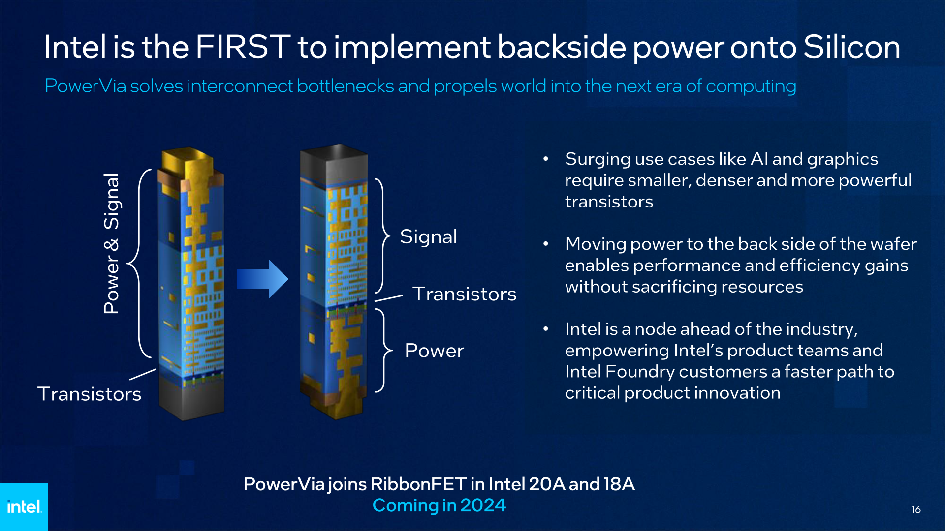
Meanwhile, this disclosure also gives us a proper look at the total number of layers involved in the two chips. Whereas a standard Intel 4 chip will have 15 layers plus the redistribution layer (RDL) all on one side, the PowerVia test chip had 14 layers on the signal (front) side, and another 4 layers plus the RDL on the power (back) side. That is a net gain of 3 layers overall, so at least as far as Intel’s test chip goes, it’s more complex in terms of the total number of layers used. But on the flip side, all of those new layers come on the power side of the chip, where they’re all relatively large and easy to fab. Which is why Intel considers the additional layers a minimal drawback compared to not having to manufacture a 30 nm pitch M0 layer.
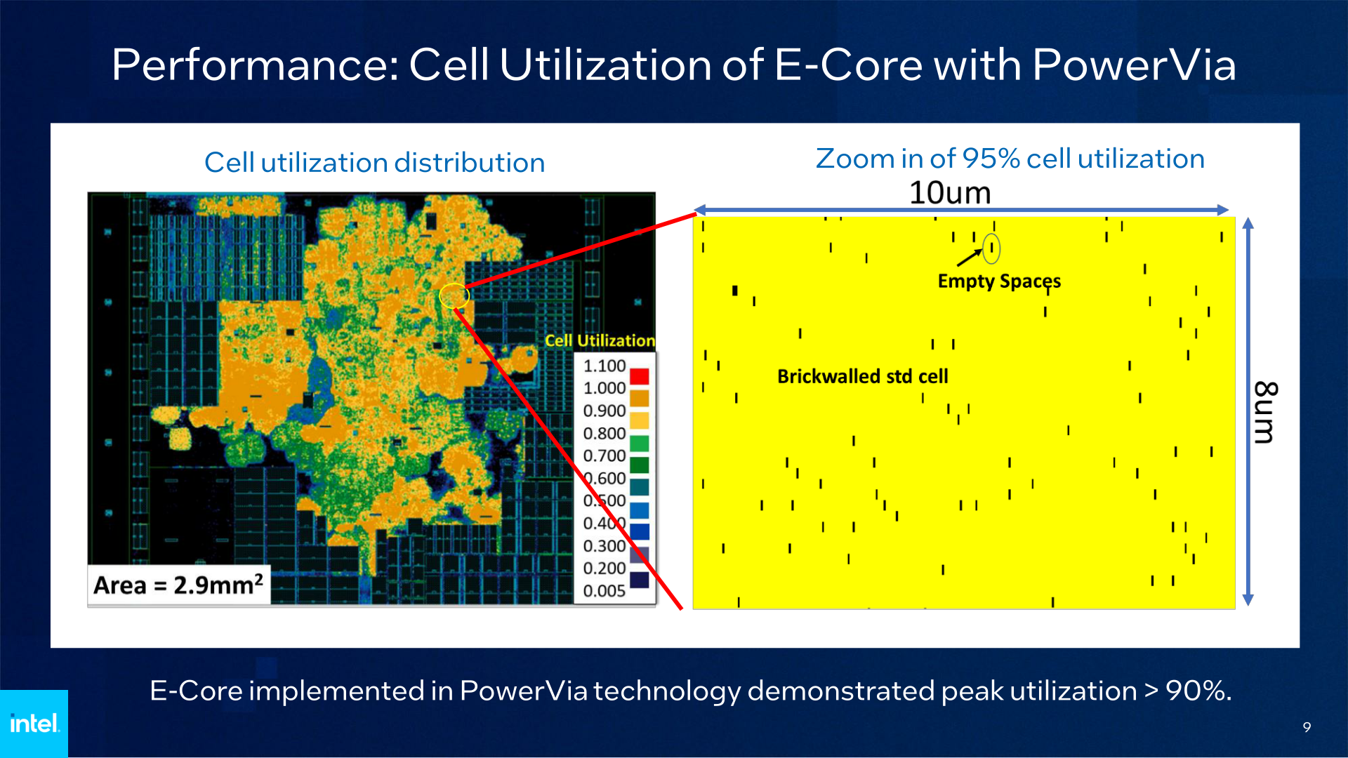
The density of these cells is also quite impressive. By moving to backside power delivery, Intel was able to utilize 95% of the space within one of the denser spots within the E-core cell. Unfortunately, Intel didn’t give comparable numbers for E-cores on Intel 4, but in general, the utilization is not quite that high.
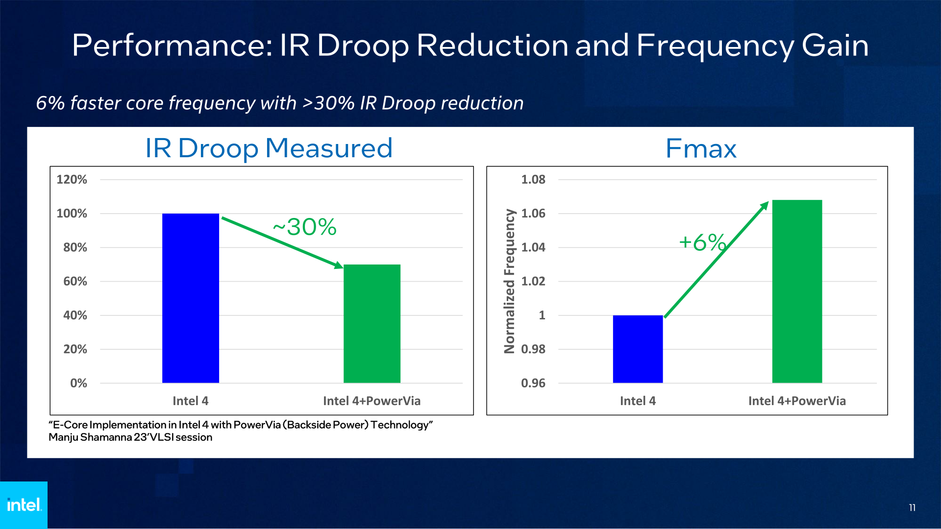
As for the electrical performance of the E-cores, as expected, PowerVia delivers a significant reduction in IR Doop. Intel measured a 30% reduction in droop on their test chip as compared to an Intel 4-built E-core, and an even greater 80% (5x) reduction in droop at the actual chip bump level.
That clean power delivery, in turn, improves the compute performance and the energy efficiency of the chip. Besides the direct efficiency gains from losing less energy to resistance, constructing an E-core with PowerVia technology improved the maximum frequency (fMax) of the core by 6%. Intel doesn’t offer a more detailed explanation as to why this improved their clockspeeds, but I suspect it has to do with a higher voltage actually reaching the transistors themselves, allowing them to clock a bit higher.
And while a 6% clockspeed uplift isn’t a massive gain, it’s essentially a “free” improvement coming from a technology that is designed to improve the manufacturability of a chip. Intel has worked harder to get smaller clockspeed improvements in the past.
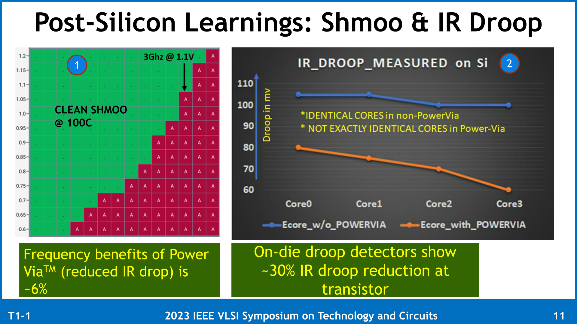
Interestingly, Intel did find that the new IR Droop values were not the same across all of the E-cores. Whereas the standard Intel 4 chip had a fairly consistent droop over all 4 cores, the droop for the test chip was between 60 mV and 80 mV, depending on the core. As this is a research presentation, Intel doesn’t go into the product ramifications of that, but assuming that production chips have a similarly wide range of variability, it may mean we see a greater emphasis on favored/prime cores in future products.
So PowerVia/BS-PDN works. But can Intel manufacture it at scale? The answer to that is also yes.
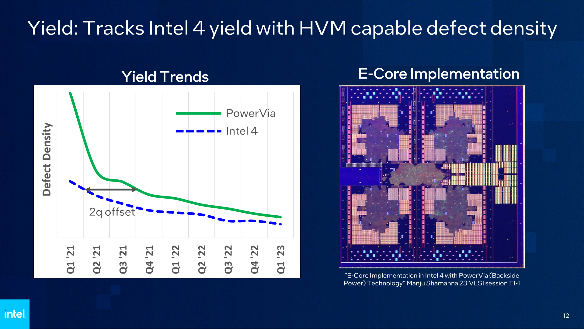
Accord to Intel, the defect density for their experimental Intel 4 + PowerVia process node is only about two quarters behind the Intel 4 process itself (which is already in HVM). Meaning that not only is the defect density low enough to be suitable for mass production in short order, but if Intel were scaling this specific node up for production, they would have similar chip yields as current, non-PowerVia Intel 4 chips in just two quarters.
Similarly, Intel reports that transistors built on the PowerVia process are very similar to those of the Intel 4 process. Which in this case, is very much a good thing, as it means those transistors aren’t doing unexpected things that impact performance or chip reliability. For that matter, Intel also noted that they observed no power-related reliability violations on the test chip, demonstrating that despite the significant changes to power delivery, the introduction of backside power delivery did not result in a less reliable power delivery system for the chip.
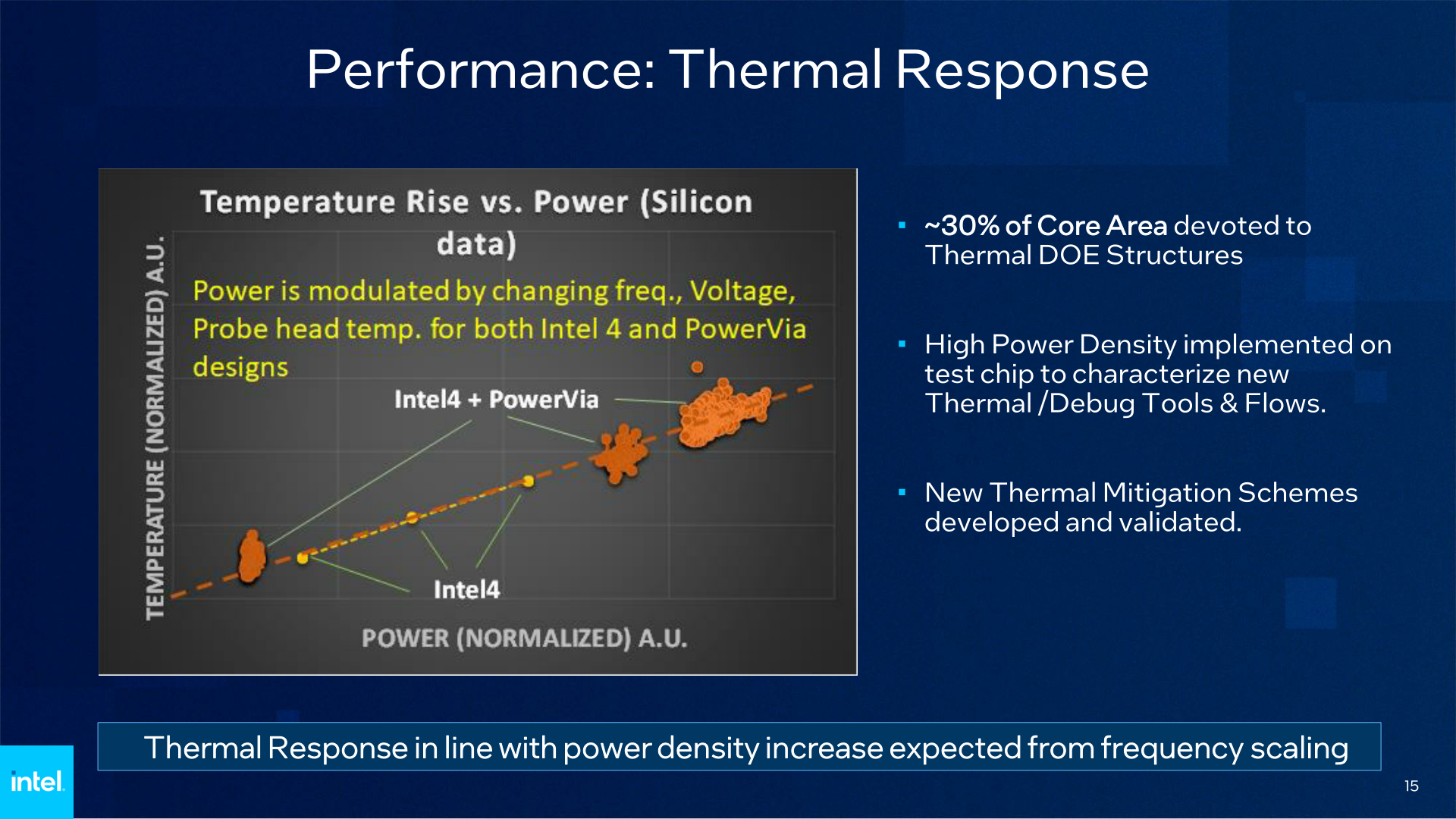
And while Intel isn’t going into the exact measures they’re employing to mitigate the thermal impacts of the transistor layer no longer being at the top of a flipped chip, the company is publishing data showing that the mitigations they have undertaken have been successful.
When plotted against the thermal response curve for an Intel 4 chip, Intel’s test chip demonstrated a very similar thermal response curve. Which is to say that at a given power level, the resulting temperatures were in-line with an Intel 4 chip. And as you may notice from Intel’s chart, they even went ahead and overfed the chip a bit to simulate even higher thermal loads, to better characterize the thermal response curve and to make sure thermal scaling wasn’t breaking down at higher thermal densities.
As noted earlier, thermals/cooling are one of the two big product-level challenges with backside power delivery. Placing transistors in what’s become the middle of the chip has not done chip cooling any favors, but Intel believes they have developed the necessary mitigation strategies to bring PowerVia chips in line with traditional frontside-fabbed flip chips.
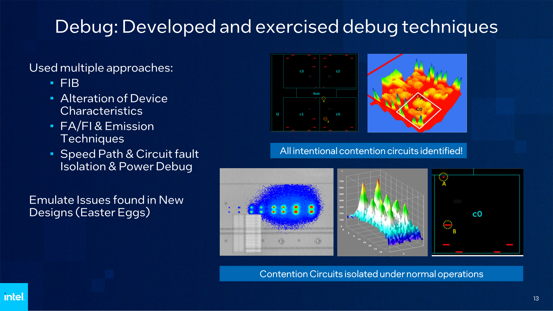
Those mitigations go for debugging, as well, which was the other challenge with BS-PDN. Intel has developed a suite of new and modified debugging techniques to deal with the fact that both sides of a chip are now in use. And while, to quote the abstract of Intel’s paper “Failure debug and defect isolation is complex due to the presence of metallization on both sides of the wafer,” ultimately, Intel was able to develop the necessary tools.
Interestingly, Intel even placed some “Easter Egg” defects within the chip’s design in order to provide some semi-controlled defects for Intel’s validation teams to work against. According to Intel their validation teams found all of those eggs with their PowerVia debugging tools, helping to prove the validity of those debug processes.
PowerVia To Land in Intel Chips in 2024
Wrapping things up, ahead of next week’s VLSI conference Intel is laying out a very convincing case that they are on the right track with their PowerVia backside power delivery technology development. Having a complex test chip up and running is a big deal in this regard, as having actual data and experience to draw from is a major step towards fine-tuning the technology for high volume manufacturing, all the while showcasing that Intel is so far meeting their aggressive fab development goals.
Ultimately, PowerVia is perhaps the single biggest make-or-break moment for Intel in terms of fully recovering momentum and potentially retaking leadership within the silicon lithography business. If Intel can deliver on its promises, the company is expecting to be at least two years ahead of TSMC and Samsung in deploying backside power delivery – and that means at least two years of reaping the cost and performance benefits of the technology. TSMC for its part is not expecting to deploy backside power until its N2P node in late 2026 or early 2027, while it remains unclear when Samsung will make their own transition.


As for Intel, if everything continues to go to plan, Intel will begin high volume manufacturing with PowerVia in 2024, when the company is scheduled to bring both its Intel 20A and Intel 18A processes online. The first consumer processor to launch using the technology will be Intel’s Arrow Lake architecture, which will be a future generation Core product built on the 20A node.


31 Comments
View All Comments
DaRagingLunatic - Monday, June 5, 2023 - link
Great article. Very informative and highly impressed. These are the types of articles that keep me coming back to anandtech. Thanks very much. I hope the back side power delivery goes well for Intel, and from this article it appears that it will, also it’s nice to get that 6% frequency boost due to a change in power delivery. With the intel 4 M0 transistor gate pitch being 30nm, and with backside power delivery they made it 36nm. Really makes me wonder just how wide they need to keep these gate pitches, in the die shrinks, and just how many transistors per mm2 we are going to run up to, and where the point of shrink will stop.name99 - Monday, June 5, 2023 - link
As usual from an Intel presentation, you get an accurate (kinda...) story about what INTEL is doing, and a completely distorted story about how this relates to the rest of the world...As far as the rest of the world goes
https://www.imec-int.com/en/articles/imec-demonstr...
Points being
- imec (and through them, essentially TSMC and SS) have already demonstrated this tech in 2021. This includes Intel's precious nanoTSV's that they're trying hard to pretend are tech exclusive to them. What's known of TSMC is that their roadmap starts with BSPDN but NOT nano-TSV's, that's for a year later; but that reflects TSMC's usual caution, one step at a time; rather than they don't know about nTSV's or can't manufacture them.
- the big win with BSPDN is not the power/voltage droop improvements. Those are nice, but only matter if you're already driving your chip at crazy power levels. No, the big win is relieving routing congestion in M1. It is this routing congestion that has throttled the down-scaling of SRAM in recent processes; and the expectation is that by moving to BSPDN (even the initial, simpler, non-nTSV version chosen by TSMC for gen1) SRAM scaling can resume. BUT for that to be of value, you have to be willing to keep the rest of your metal network in place, as low-pitch as before...
In other words, the issue is not "Intel smart, TSMC stupid"; it is priorities.
Intel's priority (for better or worse) it to be able to crank up the *effective* power and frequency of their chips even more. For them, right now, BSPDN matters insofar as it allows for slightly lower power translated into slightly higher clock.
ISMC's priorities are (a) process implementation reliability [hence two stages, BSPDN first, nTSV second a year later] and (b) denser SRAM (which they get some of, even at the first stage of BSPDN without nTSV).
IMHO the longer-term imec/TSMC strategy will also move clocks down to the backside. This will have little effect on power, but it will relieve routing even more, allowing for even denser SRAM. I have no idea, but I would not be surprised if at least part of the slow cautious TSMC strategy is to put together a process that naturally extends to moving the clocking layers to the backside, whereas the faster Intel strategy has been to ignore this and hope that, somehow, it can be retrofitted in the future...
DannyH246 - Tuesday, June 6, 2023 - link
Excellent post! Quite honestly this kind of balanced comparison of the various tech out there is what we would want in the main article. It’s a shame www.IntelTech.com hasn’t done this for a while now.drajitshnew - Wednesday, June 7, 2023 - link
@name99 impressive post.I had been confused for some time about the limitation on scaling of SRAM as traditional 6T SRAM has only transisters which are scaling. Even DRAM with Capacitors is now scaling in production to 12 nm
Quantum Mechanix - Thursday, June 8, 2023 - link
Love your explanation on what's hindering SRAM scaling, not that easy to find out there- bravo!my_wing - Sunday, June 11, 2023 - link
At first it seem like what you talking about IMEC make a bit of sense. But the longer I read from other website and other things (of course a lot still not understand). But what I can conclude is now the following.In July 2021, intel already mentioned a lot about PowerVIA, it that meant that your IMEC paper is in the same class, then TSMC is not behind. Sorry I don't get it.
Intel give us number and it also give us number of Intel 4 without PowerVIA, So now we can even draw some number out from TSMC N3 vs TSMC N5 vs Intel 4.
So the Contacted Gate Pitch is 45nm Vs 51nm Vs 50nm (lower is better).
We know that there is only Single Digit Density improvement TSMC N3E Vs TSMC N5, we know that Intel 4 is at least better then TSMC N5, we know that Intel 4 Vs Intel 4 (with PowerVIA) bring double Digit Density with 6% free frequency boost through less noise and direct connect.
i.e. Intel 4 with PowerVIA beat both TSMC N3E and TSMC N5.
After I saw this from you, I am very worry about TSMC. Because I don't know whether TSMC N2 Vs TSMC N3E will bring single digit density boost (from another Anand Article), if you look at TSMC N2 Vs Intel 4 (with PowerVIA) then you can have the same density profile, that is very bad because we will not see TSMC N2 in another 2 years (2025). I didn't see any Risk Production on TSMC N2 Today, but Intel 4 (with PowerVIA) is at Risk Production stages.
On top you mentioned small steps, i.e. the First Backside Power Delivery might not even use nTSV and Intel PowerVIA meant that is TSMC 2nd Generation Backside Power Delivery.
In my point of view, I felt like that TSMC have all the resource (even more then Intel), they did not do a de-risk and produce a N3(Backside Power Delivery) (they have some many N3 Node name already (N3B/E/P/X) is is clear they can do a N3 (Backside Power Delivery Node), that is very bad for TSMC.
If Intel pull this off and just leave GAA just rename this Intel 4 PowerVia as Intel 20A, then they already fully catch up with TSMC. This is the fact.
What TSMC is doing sound like a company in trouble.
1) Quickly talk to their customer (probably with some price cut) and sell what it can - from what nVidia say they will use TSMC still.
2) Having buzz word and tell people they start procurement and process to start something that is remotely truth. (TSMC say that they start risk production of N2 but the road map show it is H2 2025 like 2 years away and for semi industry this is long for procurement purposes).
3) Having the CEO/CFO saying to analyst that the recent profit dip is temporary and having a good long term (financial tricks) (just like Bob Swam @ Intel), and not the CTO saying we have this tech and that tech so we are good.
4) No admitting this danger and just quick dive into the technology, i.e. have a N3 with backside power delivery, and not just focus on GAA, this is a mistake. The Intel slide show that it is cheap to manufacture Intel 4 with PowerVIA (2nd slides).
5) Your competitor is show you with hard numbers (Contacted Poly Pitch is very hard number and 95% density, people can scan your chip after it is available (meteor lake is 2H 2023), there is little room to cheat, and what you give in >1.15X over TSMC N3E (another article in Anand), so what is ">" meant about/around/best case????.
In other word it is an issue of Intel being smart and TSMC is stupid. This is a Trillion Dollar Company and this is what is happen after Chang left, I am very worry, just like when Paul Otellini and Pat left Intel (I really don't think Larrabee is a failure).
Zoolook - Monday, June 12, 2023 - link
You seem to have missed that Intel is not introducing PowerVia until with 20A and thats half a year before TSMC N2, and looking back at the execution of process improvements the last 10 years between the two companies, Intel will likely still be behind, maybe a bit less but personally I doubt it.my_wing - Wednesday, June 14, 2023 - link
That is the Pre Chang TSMC, post Chang TSMC missed N3B for at least 1 year, no one except Apple is going to use N3B, and the amount of EUV exposure in N3B is way too much, so they reduced in N3E (technically without any SRAM scaling vs N5, then N3E is just a name?). Looking at the post Chang record, I can also assume that TSMC N2P is only going to come out at 202X with delays on the card. CEO is long term planning guy, it was also not day 1 when Paul Otellini left and Intel shows the sinking, it take 3 years for us to know, CEO influence often shown 3+ years and guess what Chang retired 2018, and N3B problem is in 2022 (3/4 yearish).Intel is already ahead (intel 4 is already 100% of what TSMC N3E High Performance is (3 Fins), the density side then intel did not show us or have High Density Library (2 Fins)), not behind you can be a cheerleader for TSMC, I was a TSMC shareholder and I sold that at 117 USD ADR and switch to ASML. With this intel slide, I am starting to switch from ASML to Applied Materials. I put real money to things that I talk, not a fanboy.
You can doubt it but the number 45nm Vs 51nm Vs 50nm, as far as I can see (because they all (all article from different source) say TSMC N3E will not bring density improvement over N5), might be this is not clear enough, it meant in the high performance library, TSMC N3E (next year) = Intel 4.
Intel is already 1 year ahead. As TSMC N3B is not a production ready node. Apple is consider go to N3E for iPhone 16. TSMC N3B with it's high number EUV layer + min density improve just not worth the cost. While Intel 4 with Applied Material help seem to crack to code, and their improve Intel 3 is next year, then that is second generation vs a first real N3 Class from TSMC.
tipoo - Monday, June 5, 2023 - link
Intel will see a monster turnaround through 2025-26. Only fear priced in right now.evilpaul666 - Monday, June 5, 2023 - link
They'll buy back more of their shares to pump the price a bit. Should have plenty of cash since they're getting that CHIPS Act money to pay for manufacturing upgrades.