The Solution: Accelerated Hub Architecture
Instead of having everything communicate with the memory/CPU via the PCI bus, the new Accelerated Hub Architecture allows for direct communication between the memory/CPU and disks, peripherals, and in the case of the i810 chipset, the graphics adapter.
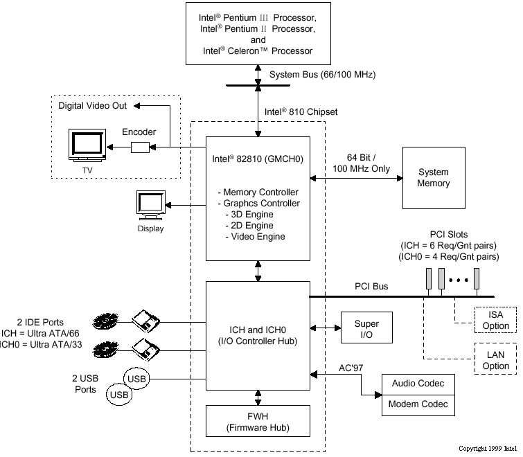
The key to the success of the Accelerated Hub Architecture is the substitution of individual hub interfaces for the PCI bus in connecting the various parts of your system to your memory/CPU on the motherboard end of things. Take a look at the acronym PCI, Peripheral Component Interconnect, it doesn't really scream "all-purpose-bus" now does it? Intel took what was once a two-chip solution (North/South Bridge) and converted it into a two chip, three-hub solution, the first implementation being the i810 chipset. The three individual hubs are the Graphics and Memory Controller Hub (GMCH), the I/O Controller Hub (ICH) and the Firmware Hub (FWH). The two main hubs, the GMCH and the ICH are connected via an internal bus that offers double the bandwidth of the PCI bus, 266MB/s. This is a definite improvement over the "old" way of doing things and will shortly become the new standard as far as chipsets go, don't expect Intel to return to the classical way of doing things on the motherboard level anytime soon.
So you have all this bandwidth to make use of, how did Intel go about making the most cost effective and integrated chipset solution in the history of the company? Let's start with the GMCH, the Graphics and Memory Controller Hub.


1 Comments
View All Comments
xrror - Monday, December 8, 2014 - link
It's amusing in retrospect how difficult it was for Intel to obsolete the older BX chipset. One thing people forget is the venerable 440BX was actually the hi-end server chipset - it wasn't intended to be the bread and butter Slot 1 mainstream chipset. But all the mobo makers migrated to BX since the "mainstream" LX, MX, ZX chipsets were just gimped too much.But if you ever wondered why BX had things like support for 1GB (!) of RAM, dual-processor, ACPI, etc that we take for granted now - that's why. It was supposed to be a server chipset ;p