IBM, NVIDIA and Wistron Develop New OpenPOWER HPC Server with POWER8 CPUs
by Anton Shilov on April 6, 2016 12:01 PM EST
IBM, NVIDIA and Wistron have introduced their second-generation server for high-performance computing (HPC) applications at the OpenPOWER Summit. The new machine is designed for IBM’s latest POWER8 microprocessors, NVIDIA’s upcoming Tesla P100 compute accelerators (featuring the company’s Pascal architecture) and the company’s NVLink interconnection technology. The new HPC platform will require software makers to port their apps to the new architectures, which is why IBM and NVIDIA plan to help with that.
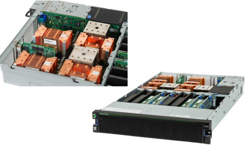
The new HPC platform developed by IBM, NVIDIA and Wistron (which is one of the major contract makers of servers) is based on several IBM POWER8 processors and several NVIDIA Tesla P100 accelerators. At present, the three companies do not reveal a lot of details about their new HPC platform, but it is safe to assume that it has two IBM POWER8 CPUs and four NVIDIA Tesla P100 accelerators. Assuming that every GP100 chip has four 20 GB/s NVLink interconnections, four GPUs is the maximum number of GPUs per CPU, which makes sense from bandwidth point of view. It is noteworthy that NVIDIA itself managed to install eight Tesla P100 into a 2P server (see the example of the NVIDIA DGX-1).

Correction 4/7/2016: Based on the images released by the OpenPOWER Foundation, the prototype server actually includes four, not eight NVIDIA Tesla P100 cards, as the original story suggested.
IBM’s POWER8 CPUs have 12 cores, each of which can handle eight hardware threads at the same time thanks to 16 execution pipelines. The 12-core POWER8 CPU can run at fairly high clock-rates of 3 – 3.5 GHz and integrate a total of 6 MB of L2 cache (512 KB per core) as well as 96 MB of L3 cache. Each POWER8 processor supports up to 1 TB of DDR3 or DDR4 memory with up to 230 GB/s sustained bandwidth (by comparison, Intel’s Xeon E5 v4 chips “only” support up to 76.8 GB/s of bandwidth with DDR4-2400). Since the POWER8 was designed both for high-end servers and supercomputers in mind, it also integrates a massive amount of PCIe controllers as well as multiple NVIDIA’s NVLinks to connect to special-purpose accelerators as well as the forthcoming Tesla compute processors.
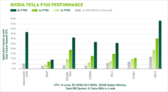
Each NVIDIA Tesla P100 compute accelerator features 3584 stream processors, 4 MB L2 cache and 16 GB of HBM2 memory connected to the GPU using 4096-bit bus. Single-precision performance of the Tesla P100 is around 10.6 TFLOPS, whereas its double precision is approximately 5.3 TFLOPS. A HPC node with eight such accelerators will have a peak 32-bit compute performance of 84.8 TFLOPS, whereas its 64-bit compute capability will be 42.4 TFLOPS. The prototype developed by IBM, NVIDIA and Wistron integrates four Tesla P100 modules, hence, its SP performance is 42.4 TFLOPS, whereas its DP performance is approximately 21.2 TFLOPS. Just for comparison: NEC’s Earth Simulator supercomputer, which was the world’s most powerful system from June 2002 to June 2004, had a performance of 35.86 TFLOPS running the Linpack benchmark. The Earth Simulator consumed 3200 kW of POWER, it consisted of 640 nodes with eight vector processors and 16 GB of memory at each node, for a total of 5120 CPUs and 10 TB of RAM. Thanks to Tesla P100, it is now possible to get performance of the Earth Simulator from just one 2U box (or two 2U boxes if the prototype server by Wistron is used).
IBM, NVIDIA and Wistron expect their early second-generation HPC platforms featuring IBM’s POWER8 processors to become available in Q4 2016. This does not mean that the machines will be deployed widely from the start. At present, the majority of HPC systems are based on Intel’s or AMD’s x86 processors. Developers of high-performance compute apps will have to learn how to better utilize IBM’s POWER8 CPUs, NVIDIA Pascal GPUs, the additional bandwidth provided by the NVLink technology as well as the Page Migration Engine tech (unified memory) developed by IBM and NVIDIA. The two companies intend to create a network of labs to help developers and ISVs port applications on the new HPC platforms. These labs will be very important not only to IBM and NVIDIA, but also to the future of high-performance systems in general. Heterogeneous supercomputers can offer very high performance, but in order to use that, new methods of programming are needed.
The development of the second-gen IBM POWER8-based HPC server is an important step towards building the Summit and the Sierra supercomputers for Oak Ridge National Laboratory and Lawrence Livermore National Laboratory. Both the Summit and the Sierra will be based on the POWER9 processors formally introduced last year as well as NVIDIA’s upcoming code-named Volta processors. The systems will also rely on NVIDIA’s second-generation NVLink interconnect.
Image Sources: NVIDIA, Micron.
Source: OpenPOWER Foundation


50 Comments
View All Comments
Pinn - Wednesday, April 6, 2016 - link
Any reason not to use ARM64?questionlp - Wednesday, April 6, 2016 - link
My guess is that they are targeting the high-end HPC workloads, which is where IBM POWER and x86 processors currently reign. Both also can provide large I/O bandwidth (memory and interconnect) that is required to feed the beasts.While there are a couple of ARM64 processors being designed that can scale up in speed and I/O, those processors are not out yet; and, the ones that are out, don't meet the I/O requirements or provide enough compute horsepower. The best bet would be for someone (maybe NVIDIA?) to build something like a 8 or 16 core ARM64 processor with native NVLink and >= 40GbE or 40Gb IB)
Not to mention, power consumption of an IBM POWER8 or a pair of Broadwell Xeons is still relatively small compared to 4, 8 or 16 of those NVIDIA compute modules.
Pinn - Wednesday, April 6, 2016 - link
Makes sense. Would love to see that combination arm64 and pascal/volta. Thanks!Ktracho - Wednesday, April 6, 2016 - link
I'm not sure how you could make a business case for something like that, given the huge development and support cost and how small the market would be. Of course, there's Tegra, but I doubt that's what you're referring to.Brutalizer - Wednesday, April 6, 2016 - link
"Each POWER8 processor supports up to 1 TB of DDR3 or DDR4 memory with up to 230 GB/s sustained bandwidth (by comparison, Intel’s Xeon E5 v4 chips “only” support up to 76.8 GB/s of bandwidth with DDR4-2400).""My guess is that they are targeting high-end HPC workloads, which is where IBM POWER and x86 processors currently reign. Both also can provide large I/O bandwidth (memory and interconnect) that is required to feed the beasts."
-------------------------------------------------
Wow! 230 GB/sec sustained bandwidth for POWER8 is really a brutal number! And the x86 supports 80 GB/sec which is also good. The SPARC M7 only states only 160 GB/sec bandwidth in the specs.
Let us look at memory bandwidth benchmarks, and not a theoretical number. How well do they perform in real benchmarks? In official STREAM benchmarks, we see that
https://blogs.oracle.com/BestPerf/entry/20151025_s...
-POWER8 gets 320 GB/sec for a 4-socket system. This translates to 80 GB/sec for one POWER8 cpu. Quite far away from the stated "230GB/sec sustained memory bandwidth", eh?
-E5-2699v3 gets 112 GB/sec for a 2 socket system. This gives 56 GB/sec per x86 cpu.
-SPARC M7 cpu gets 145 GB/sec which is close to the stated number of 160 GB/sec.
Who do you think is most "dishonest" with their numbers? Oracle?
"...IBM says the sustained or delivered bandwidth of the IBM POWER8 12-core chip is 230 GB/s. This number is a peak bandwidth calculation: 230.4 GB/sec = 9.6 GHz * 3 (r+w) * 8 byte. A similar calculation is used by IBM for the POWER8 dual-chip-module (two 6-core chips) to show a sustained or delivered bandwidth of 192 GB/sec (192.0 GB/sec = 8.0 GHz * 3 (r+w) * 8 byte). Peaks are the theoretical limits used for marketing hype, but true measured delivered bandwidth is the only useful comparison to help one understand delivered performance of real applications...."
Brutalizer - Wednesday, April 6, 2016 - link
IBM states that POWER8 has 230 GB/sec _sustained_ bandwidth, by looking at the peak theoretical bandwidth of 230.4 GB/sec. I dont really know when peak theoretical bandwidth became the same thing as sustained bandwidth? In real life benchmarks we see that IBM POWER8 reaches 80 GB/sec, that is 1/3 of their stated number. And someone called Oracle benchmarks "dishonest". Hmmm...Brutalizer - Wednesday, April 6, 2016 - link
BTW, when Oracle uses 16 GB dimms, SPARC M7 reaches 169 GB/Sec in real life benchmarks. Just look at the bottom of the link I provided. It is quite close to the stated bandwidth of 160 GB/sec.JohnMirolha - Wednesday, April 6, 2016 - link
Let's use math.Let's assume a standard 160GB/s per socket with a 12 coreCPU vs the same BW with a 32 core CPU.
Which system will provide better performance at the core level ?
Now let's throw some GPUs, because, you know, HPC does not run Oracle and makes great use of them.
Now, to make things more interesting, let's use Linux for HPC ... because, you know, they mostly run on Linux not Solaris.
SPARC M = irrelevant
Brutalizer - Thursday, April 7, 2016 - link
Well, one socket with TWO power8 cpus reaches 160GB/sec (read my post on page2), just the same as one SPARC M7. So the SPARC M7 has at least twice the memory bandwidth. The POWER8 S822L server has two sockets, but four POWER8 cpus. And if you look at benchmarks, the POWER8 is slower than x86. Whilst being more expensive. That is quite bad.https://blogs.oracle.com/BestPerf/entry/201510_spe...
SarahKerrigan - Friday, April 8, 2016 - link
Entry P8 systems use a DCM for cost reasons. Since each die in the DCM has half its memory controllers enabled, the memory performance is effectively identical to the SCM used in other P8 systems.Of course, you knew this, since you've been told it at length at RWT and other places - but don't let me get in the way of your multi-decade Sun/Oracle promotion...