Samsung and TSMC Roadmaps: 8 and 6 nm Added, Looking at 22ULP and 12FFC
by Anton Shilov on May 5, 2017 9:30 AM EST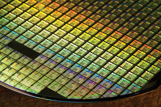
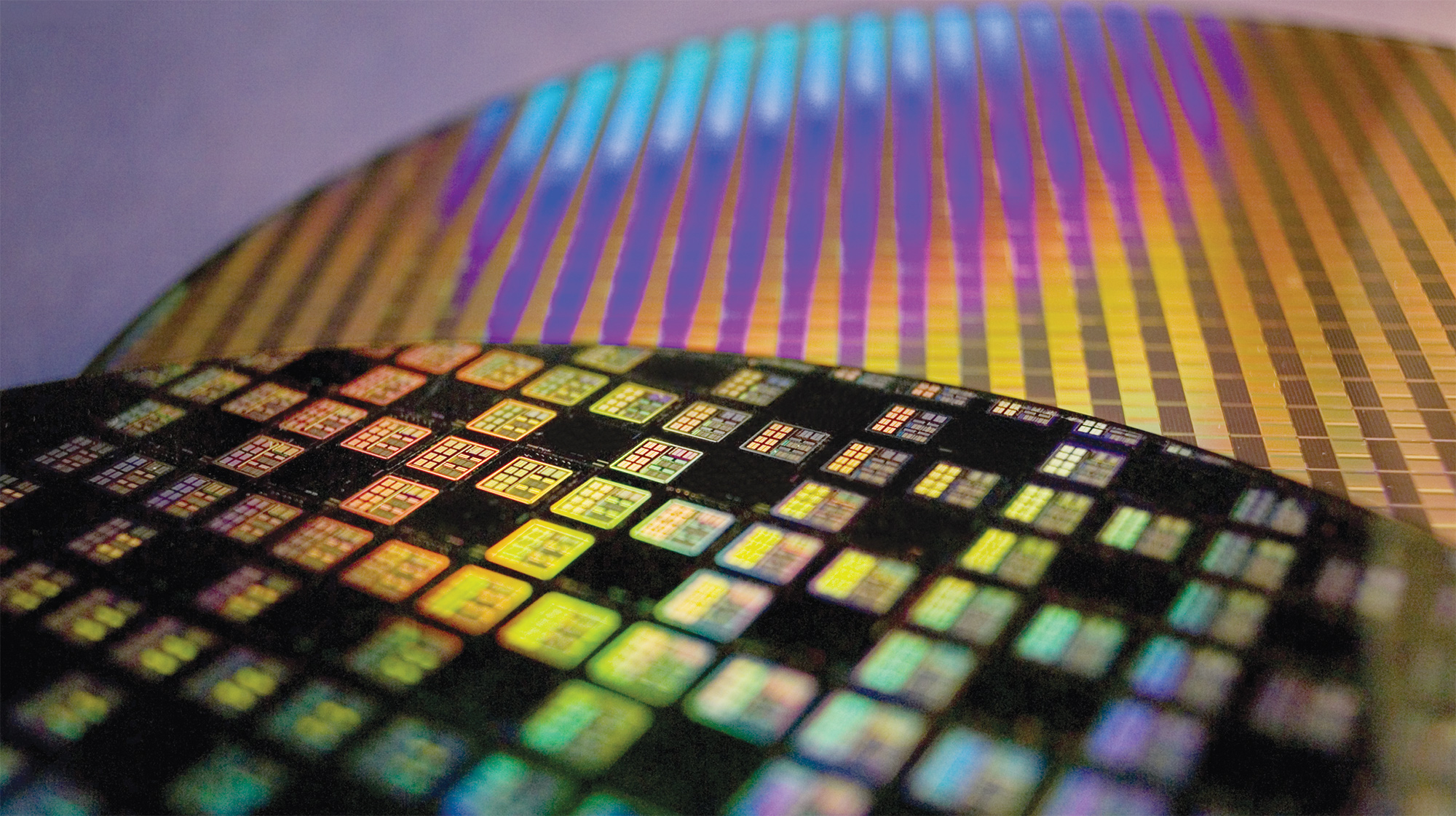
Samsung and TSMC made several important announcements about the present and future of their semiconductor manufacturing technologies in March. Samsung revealed that it had shipped over 70 thousand wafers processed using its first-generation 10 nm FinFET fabrication process (10LPE) and also announced major additions to its upcoming manufacturing technology roadmap. In particular, the company plans to introduce three processes it has not talked about thus far. TSMC said that it is about to start mass production of ICs (integrated circuits) using its first-gen 10 nm technology and also announced several new processes that will be launched in the coming years, including its first 7 nm EUV process due in 2019.
10 nm: Samsung Is Shipping

Update 5/12: Samsung informed us that its press release from October, 2016, compares characteristics of the 10LPE manufacturing technology with those of the 14LPE, not 14LPP. The text and table have been updated accordingly.
Samsung said it had started to make SoCs using its 10LPE fabrication technology last October, which is something we already knew. This manufacturing process allowed the company to make its chips 30% smaller compared to ICs made using its 14LPE process as well as reducing power consumption by 40% (at the same frequency and complexity) or increase their frequency by 27% (at the same power and complexity). So far, Samsung has processed over 70 thousand wafers using its 10LPE technology, which can give an idea about Samsung’s 10 nm production capacities (considering that the whole 10 nm production cycle is greater than the 90 days we saw with previous-gen FinFET processes). At the same time, keep in mind that Samsung does not have many 10 nm designs to manufacture right now: we know only of the company’s own Exynos 9 Octa 8895 as well as Qualcomm’s Snapdragon 835 seen in the Samsung Galaxy S8.
| Advertised PPA Improvements of New Process Technologies Data announced by companies during conference calls, press briefings and in press releases |
||||||||
| GF | Samsung | |||||||
| 7nm DUV vs 14LPP |
14LPP vs 28LPP |
10LPE vs 14LPE |
10LPE vs 14LPP |
10LPP vs 10LPE |
10LPU vs 10LPE |
|||
| Power | >60% | 60% | 40% | 30% | ~15% | ? | ||
| Performance | >30% | 40% | 27% | >10% | ~10% | ? | ||
| Area Reduction | >50% | 50% | 30% | 30% | none | ? | ||
In addition to its production milestone, Samsung also confirmed plans to start mass production of chips using its second-generation 10 nm manufacturing process called 10LPP (10 nm low-power plus) by the end of 2017 as well as its third-generation 10 nm technology called 10LPU by the end of 2018. Samsung said last year that the 10LPP is going to enable a ~10% performance increase (at the same power and at the same complexity) versus the 10LPE, but we know absolutely nothing about the 10LPU. It is logical to assume that the 10LPU will bring certain PPA-related (performance, power, area) improvements, but it is not clear how Samsung plans to achieve them and which one of the three will be the focus for improvements. As it appears, just like Intel, Samsung has ended up with three generations of 14 nm fabrication processes and is going to end up with three generations of 10 nm manufacturing technologies. It is noteworthy that Samsung itself does not use its 14LPC (low-power compact) for its leading edge SoCs, which may suggest that the 10LPU is also not aimed at this segment of the market. In fact, it is highly likely that the 10LPU will target ultra-small and ultra-low-power ICs for various emerging devices, but Samsung yet has to confirm that.
10nm: TSMC Is Steady
As for TSMC, its 10 nm process technology (CLN10FF) is now qualified for production at the company’s GigaFabs 12 and 15, where high-volume ramp is expected to start in H2 2017. Production capacity of these two fabs is hundreds of thousands wafer starts per quarter and TSMC plans to ship 400 thousand wafers processed using its 10 nm manufacturing tech this year. Considering the long production cycles for FinFET-based technologies, it is about time for TSMC to start ramping up 10 nm so to be able to supply enough chips to its main customer in time. Apple is expected to launch its new iPhone products in September or October and needs to get SoCs couple of months before the launch.
| Advertised PPA Improvements of New Process Technologies Data announced by companies during conference calls, press briefings and in press releases |
|||||||
| TSMC | |||||||
| 16FF+ vs 28HPM |
16FF+ vs 20SOC |
10FF vs 16FF+ |
7FF vs 16FF+ |
7FF vs 10FF |
|||
| Power | 70% | 60% | 40% | 60% | <40% | ||
| Performance | 65% | 40% | 20% | 30% | ? | ||
| Area Reduction | ~50% | none | >50% | 70% | >37% | ||
PPA advantages of TSMC’s CLN10FF over its CLN16FF+ (second-gen 16 nm) have been discussed already and they are significant for developers of mobile SoCs (but not that significant for makers of other ICs): a ~50% higher transistor density, a 20% performance improvement at the same power and complexity or a 40% lower power consumption at the same frequency and complexity. Unlike Samsung, TSMC does not seem to plan multiple generations of 10 nm and will go straight to 7 nm next year. 7nm is currently very popular among chip designers, indicating a future major milestone. However, in addition to the CLN7FF, the company will also offer several other manufacturing technologies for ultra-small and ultra-low-power applications.


89 Comments
View All Comments
Demon-Xanth - Friday, May 5, 2017 - link
A silicon atom's width is about 110pm, so they are literally going into widths that are only double digit numbers of atoms wide.MananDedhia - Friday, May 5, 2017 - link
Processes that deposit single atomic layers are already used commonly in processes - even in 28nm.....For some layers, atomic layer deposition is the only way to go. The complexity increased here because we are now increasing the number of layers and devices that need to be defined at those scales.bug77 - Friday, May 5, 2017 - link
Yes, but you can't take 3 atoms, call then source, drain and gate and assemble them into a transistor.ddriver - Friday, May 5, 2017 - link
Why not? IBM have already demoed atomic assembly. The downside - it is very slow, it is one atom at a time VS etching septillions of atoms with acid at the same time.BTW I finally get how they will get to 5 nm - by lying about it. How much of a 10nm chip's features are at 10nm resolution? Not many. Area decrease is already falling behind the process scale number and it is only going to get worse.
On the upside - no biggie - we already have enough performance to run terminators. So our extinction is well assured.
philehidiot - Friday, May 5, 2017 - link
Don't you go worrying about terminators. I've already started work on the first of many. I was just so sick of not being able to get a seat on the bus. Was thinking no one wants to sit next to a cybernetic killing machine so I can send that to the earliest bus stop, get it to reserve a seat and I can ride to work without the smell of unwashed, practically rotting human being next to me.Far safer than one of those self driving car things. Bloody death traps.
Kevin G - Sunday, May 7, 2017 - link
Are you Sarah Conner?Xajel - Sunday, May 7, 2017 - link
Yeah they're actually moving these actual atoms... atom by atom like a legoKevin G - Sunday, May 7, 2017 - link
The node size is mostly marketing now which is why Intel went out of their way to define some new metrics ~6 weeks ago. While I wasn't a fan of that marketing spiel, there is a point that there needs to be a new metric as traditional node shrinks are few and far between going forward.What I think the foundries are waiting on is a new big break through as they realize that they cannot currently continue on the existing path indefinitely. Germanium can come in as an exotic material as a substitute for silicon but wafer prices are extremely expensive. Even then, germanium doesn't even solve the node problem but rather just provides better material properties at existing nodes. Carbon nanotubes and graphene are two related materials seen as potential for replacing silicon as we get even closer to the atomic level. Both have some good properties for circuit design but no one has found a means of economical mass production.
Both Intel and IBM has invested heavily into silicon photonics. So far their efforts have lead to advancements in IO but not raw processing but optical logic gates do exist. Much like other exotic solutions, these suffer from mass production problems to bring them out of the research lab. (Notice a trend starting here?)
I think strategies like interposers and EMIB are emerging to side step the absolute need for shrinks in the sense of limiting transistor counts. Granted interposers/EMIB do nothing with regards to power consumption. The one nice thing about these techniques is that they do potentially allow for mixing some of the more exotic solutions with bulk processes. For example, a die with slicon photonics could interface with some high speed optical circuits in the package and also interfaces with more traditional bulk processes for its SRAM cache. Very expensive but worth considering when there are other new node alternatives available. Granted, such choices are not going to happen tomorrow but they're clearly on the horizon.
eachus - Sunday, October 1, 2017 - link
My read is that the first application of nanotubes or graphene will be laying down a copper layer, then growing graphene on top of it. The trick will be to get the graphene to align on top of the copper, which will probably take another layer in between, perhaps silver. Could silver be substituted for copper in bulk? Good question. It is a better conductor and solves the alignment problem.You may think of silver as a precious metal along with gold and platinum, but over fifty per cent of the silver mined goes into silver solder for brazing or soldering metals together. Most silver solder is used for brazing, go figure. Silver is also used in thermal compounds for getting a good seal between a CPU chip and the heat sink. Obviously replacing a few grams of copper with silver inside the chip won't raise prices significantly.
Getting copper to bond to the graphene is not a problem--even if the reverse is a significant problem. However high-temperature processes may damage the graphene. Best is probably a "wet" process to put a thin layer of copper on the graphene before building the next litho layer. Putting the graphene in a copper sandwich like this should significantly improve the characteristics of the layer. This will show up as a reduced capacitance with adjacent conducting traces--less cross-talk and faster signal propagation.
beginner99 - Monday, May 8, 2017 - link
"BTW I finally get how they will get to 5 nm - by lying about it"Process tech numbering hasn't been about feature size for the past 2 decades.