SK Hynix Launches 96-Layer 3D NAND and Discloses QLC Plans
by Anton Shilov on November 8, 2018 1:00 PM EST
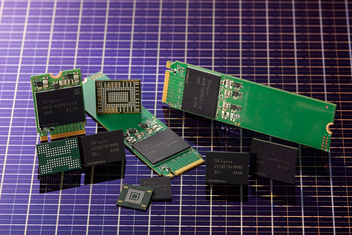
SK Hynix this week officially launched its new 96-layer 3D NAND flash memory chips, which feature a new architecture and a faster interface. The NAND has already been qualified for SSDs, with first 1 TB consumer models launching shortly and enterprise-grade solutions following on later. What is noteworthy is that these drives are going to be based on SK Hynix’s own controllers. In addition, SK Hynix will eventually offer UFS 3.0-based mobile storage devices featuring the same memory.
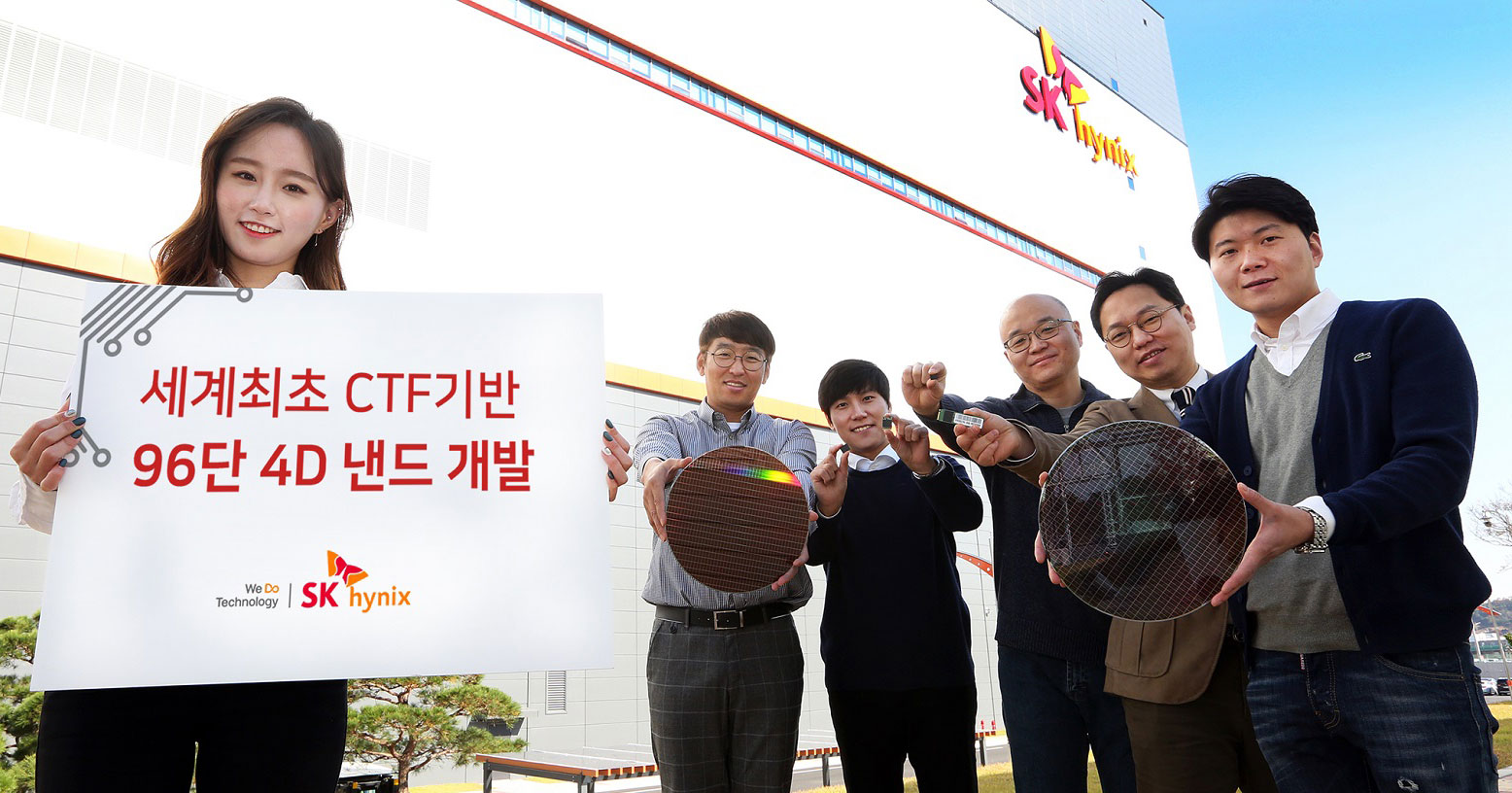
SK Hynix’s 3D-V5 NAND Memory About to Hit Mass Production
Initially available in a 512 Gb capacity, SK Hynix’s new 96-layer 3D TLC NAND memory devices are based on a charge trap flash (CTF) design with a peripheral circuits under cells (PUC) architecture. Officially the company has started referring to these devices as “4D NAND” (as announced back at Flash Memory Summit in August), though the technology is not fundamentally different from current 3D NAND architectures.
The new 3D-V5 devices use a 1.2 Gbps Toggle 3.0 I/O interface, which is faster than SK Hynix’s 72L 3D-V4 generation products. Meanwhile the chip also features a 64 KB page size (the smallest area of the flash memory that can be written in a single operation) and an 18 MB block size (the smallest area of the flash memory that can be erased in a single operation), which will further speed up performance of the new 3D-V5 devices compared to its predecessors.
SK Hynix says that the increased number of layers and its PUC architecture makes its 96-layer 512 Gb 3D NAND devices around 30% smaller versus their similar 72-layer 512 Gb 3D NAND devices. Furthermore, it can now produce wafers containing 49% more bits than before (assuming the same yield), albeit at the cost of extra process steps. Speaking of production, the company hopes to kick off “the early stage of mass production” this year. At least some of the new chips will be made at the company’s recently built M15 fab.
1 Tb 96L 3D TLC and 3D QLC NAND Chips Incoming
After SK Hynix refines the mass production of its 96L 3D TLC NAND chips, the company will move on to the next stage. Sometime next year the company plans to roll out 96L 3D NAND chips with a 1 Tb (128 GB) capacity, with both TLC and QLC variants planned.
Consumer, Enterprise SSDs Incoming, UFS 3.0 Storage Planned
SK Hynix has already validated its 96L 512 Gb 3D TLC NAND for SSDs. The company plans to release 1 TB client SSDs featuring the memory and its own controllers/firmware “within this year”. Meanwhile, enterprise-grade drives based on the same memory are due in the second half of 2019.
In addition to SSDs, SK Hynix intends to release UFS 3.0-based 96L 512 Gb 3D TLC NAND chips in the first half of next year. These will be the company’s first UFS 3.0-supporting devices and will enable it to address various high-end smartphones.
Related Reading:
- Flash Memory Summit 2018, SK Hynix Keynote Live Blog: NAND Development
- SK Hynix Announces SSDs with 72-Layer 3D NAND ICs, Own Controllers
- Klevv Adds Kolors: RGB-Lit Enthusiast-Class Cras DIMMs & SSD Incoming
- KLEVV Launches NEO N500 SSDs Based on SK Hynix’s 72-Layer 3D NAND
Source: SK Hynix


4 Comments
View All Comments
Targon - Thursday, November 8, 2018 - link
Will they ever make DDR4 3200CL14 memory, or will that stay out of their reach?ajp_anton - Thursday, November 8, 2018 - link
What does the "4D" mean in the last image?Ryan Smith - Thursday, November 8, 2018 - link
"Initially available in a 512 Gb capacity, SK Hynix’s new 96-layer 3D TLC NAND memory devices are based on a charge trap flash (CTF) design with a peripheral circuits under cells (PUC) architecture. Officially the company has started referring to these devices as “4D NAND” (as announced back at Flash Memory Summit in August), though the technology is not fundamentally different from current 3D NAND architectures."TechnoMagi - Friday, November 9, 2018 - link
So, basically a marketing campaign not based in reality. I know it make seem like a small thing, but whatever happened to good old fashioned honesty? I don't know about anyone else. But there is nothing in all the world more attractive than genuine sincerity to me. Be it in business, friendship, or love.